
Abstract
Introduction
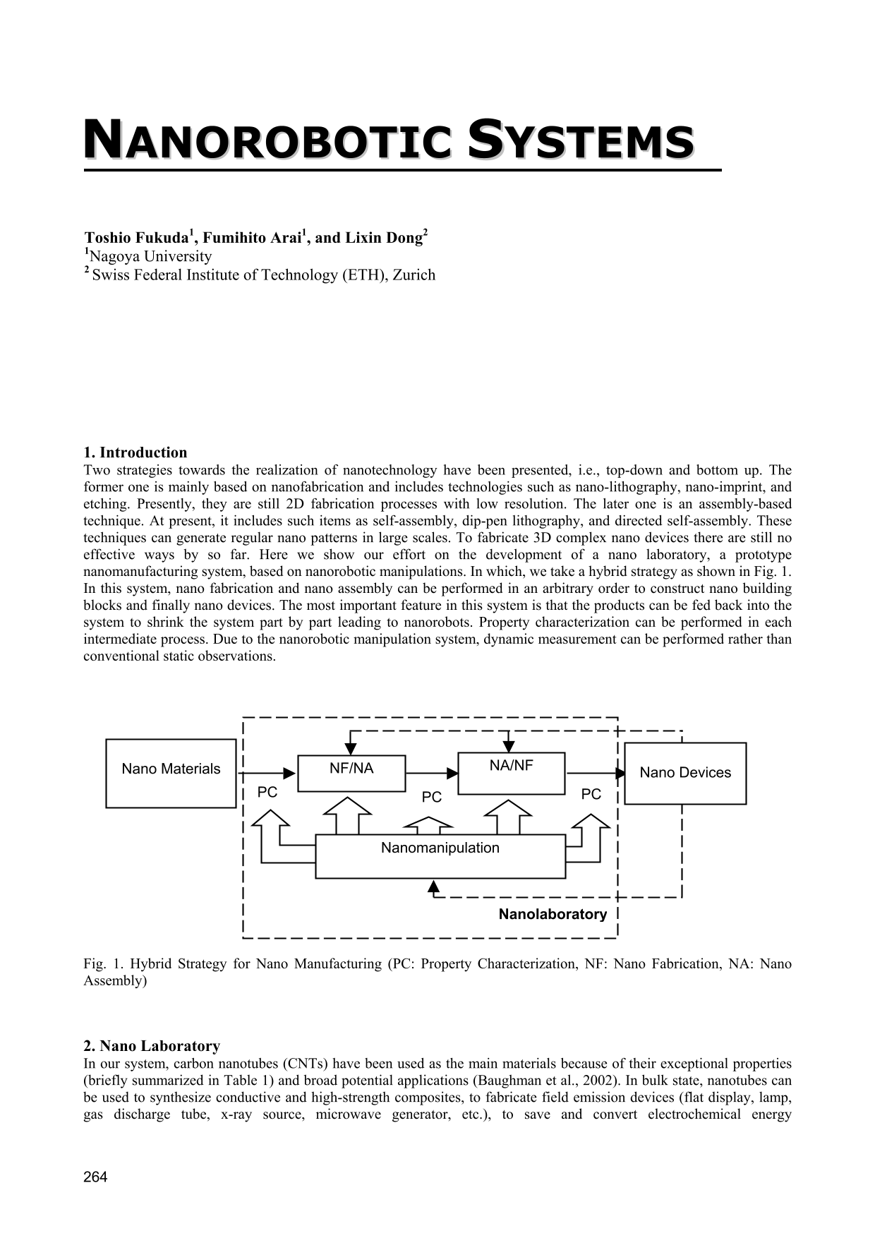
Two strategies towards the realization of nanotechnology have been presented, i.e., top-down and bottom up. The former one is mainly based on nanofabrication and includes technologies such as nano-lithography, nano-imprint, and etching. Presently, they are still 2D fabrication processes with low resolution. The later one is an assembly-based technique. At present, it includes such items as self-assembly, dip-pen lithography, and directed self-assembly. These techniques can generate regular nano patterns in large scales. To fabricate 3D complex nano devices there are still no effective ways by so far. Here we show our effort on the development of a nano laboratory, a prototype nanomanufacturing system, based on nanorobotic manipulations. In which, we take a hybrid strategy as shown in Fig. 1. In this system, nano fabrication and nano assembly can be performed in an arbitrary order to construct nano building blocks and finally nano devices. The most important feature in this system is that the products can be fed back into the system to shrink the system part by part leading to nanorobots. Property characterization can be performed in each intermediate process. Due to the nanorobotic manipulation system, dynamic measurement can be performed rather than conventional static observations.
Hybrid Strategy for Nano Manufacturing (PC: Property Characterization, NF: Nano Fabrication, NA: Nano Assembly)
In our system, carbon nanotubes (CNTs) have been used as the main materials because of their exceptional properties (briefly summarized in Table 1) and broad potential applications (Baughman et al., 2002). In bulk state, nanotubes can be used to synthesize conductive and high-strength composites, to fabricate field emission devices (flat display, lamp, gas discharge tube, x-ray source, microwave generator, etc.), to save and convert electrochemical energy (supercapacitor, battery cathode, electromechanical actuator, etc.), to store hydrogen, and so on. However, the most promising applications of nanotubes that has deepest implications for molecular nanotechnology need to maneuver the tubes individually to build complex nanodevices. Such devices include nanoelectronics and nanoelectromechanical systems (NEMS) (concisely listed in Table 2). Almost all of such applications and many unlisted potential ones of nanotubes for nanoelectronics and NEMS involve charactering, placing, deforming, modifying, and/or connecting nanotubes. Although chemical synthesis may provide a way for patterned structure of nanotubes in large-scale, self-assembly may generate better regular structures, we still lack of capability to construct irregular complex nanotube devices. Nanomanipulation (Eigler & Schweizer, 1990), especially nanorobotic manipulation (Yu et al., 1999; Dong et al., 2000; Dong et al., 2001a; Dong et al., 2001b; Dong et al., 2002b), with its “bottom up” nature, is the most promising way for this purpose.
Property of CNTs

Property of CNTs
Applications of CNTs in Nano Devices

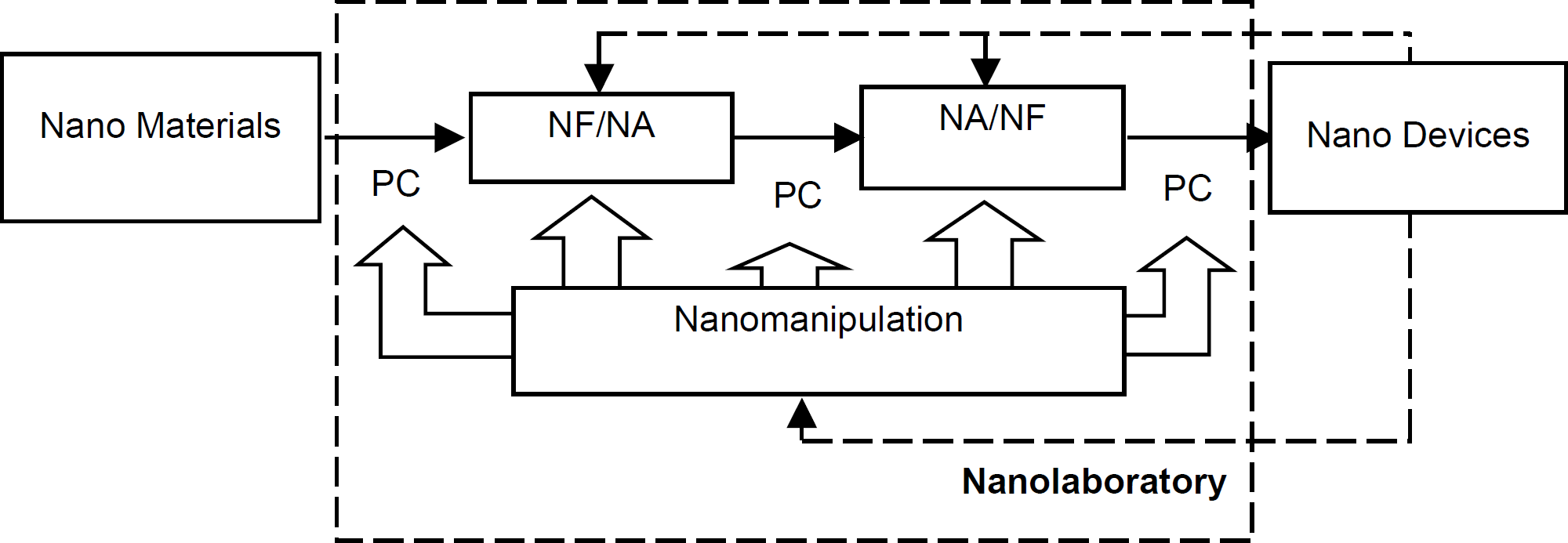
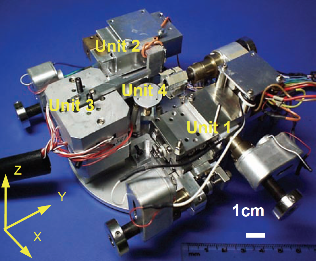
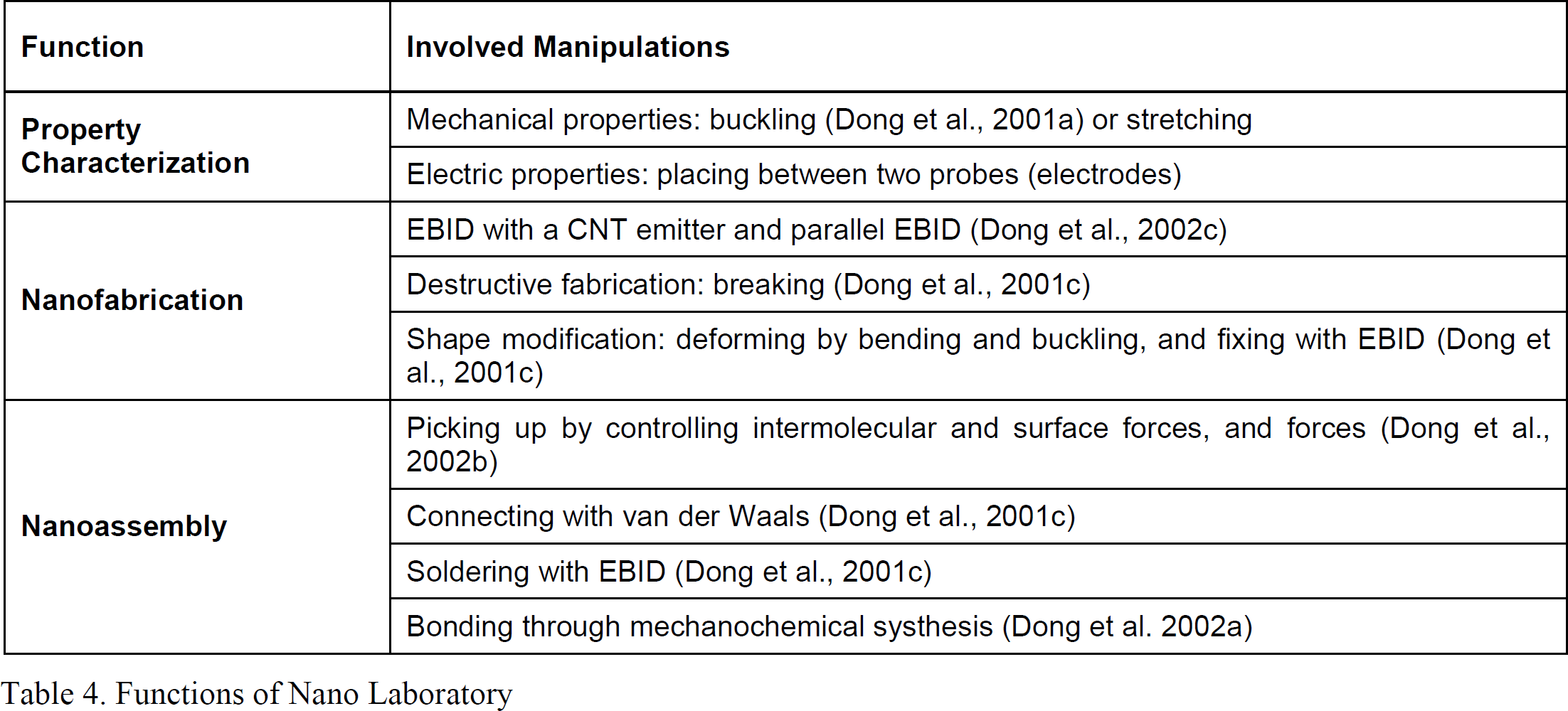
A nano laboratory is presented as shown in Fig. 2, which consists of a nanorobotic manipulation system (Fig. 3), an instrumentation system (a filed emission scanning electron microscope (FESEM) and a conventional atomic force microscope cantilever or a piezolever), and a nanofabrication system based on electron-beam-induced deposition (EBID) or manipulations. The specifications of the nano laboratory are listed in Table 3. The nano laboratory can be applied for manipulating nano materials—mainly but not limited to CNTs, fabricating nano building blocks, assembling nano devices, in situ analyzing the properties of such materials, building blocks and devices. The functions of it are summarized in Table 4, and many have been demonstrated elsewhere as shown in the references in the table.

Nano Laboratory
Nanorobotic Manipulators
Specifications of Nano Laboratory
Functions of Nano Laboratory
Interest in creating functional devices at nanometer scales is fueled by the desire to shrink the size of electronic integrated circuits and to create electromechanical systems at nanoscale. CNTs are one of the most important nanomaterials for the fabrication of NEMS including sensors and actuators because of their exceptional properties and special structures.
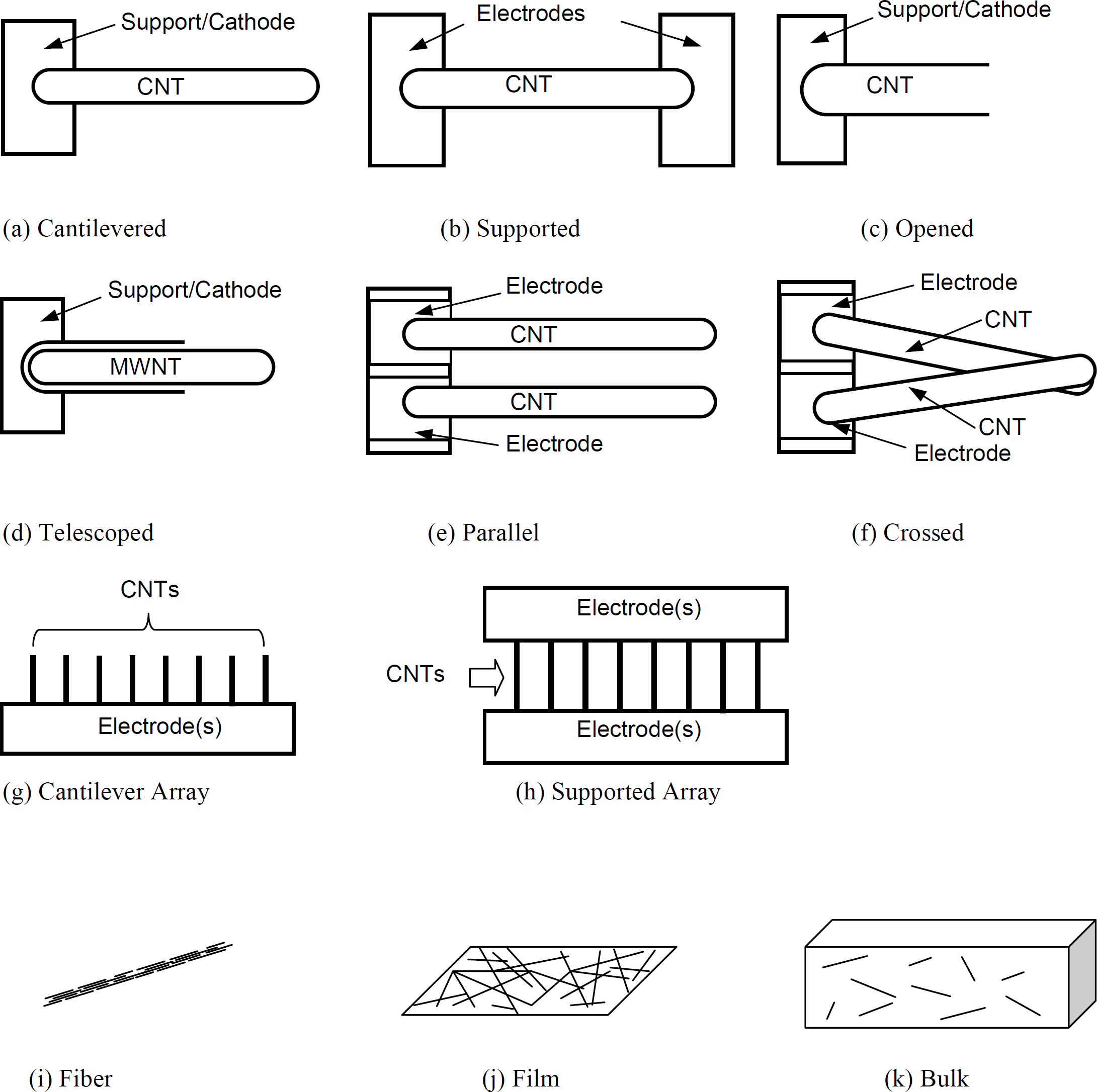
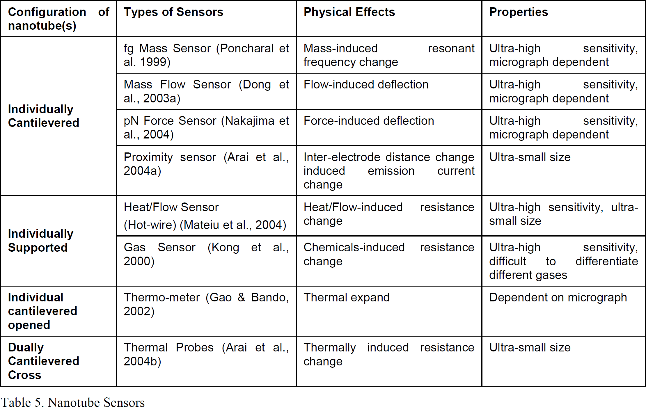
Nanotube sensors and actuators can be constructed with many configurations (as shown in Fig. 4) based on various physical and chemical properties/effects (Tables 5 and 6).
Configurations of Nanotube Sensors and Actuators
Nanotube Sensors
Nanotube Actuators

For detecting deep and narrow features on a surface, cantilevered individual nanotubes (Fig. 4 (a)) have been demonstrated as probe tips for an atomic force microscope (AFM), a scanning tunneling microscope (STM) and other kinds of scanning probe microscopes (SPM) (Dai et al., 1996) because of their ultra-small diameters, ultra-large aspect ratios, and excellent elasticity. Cantilevered nanotubes have also been shown as probes for the measurement of ultra-small physical quantities, such as femto-gram mass (Poncharal et al. 1999), mass flow sensors (Dong et al., 2003a), and pico-Newton order force sensors (Nakajima et al., 2004) on the basis of their static deflections or change of resonant frequencies detected with an electron microscope. However, the deflections cannot be measured from micrographs in real-time, which limit the application of this kind of sensors. Inter-electrode distance change caused emission current variation of a nanotube emitter may serve as a candidate to replace the microscope images (Arai et al., 2004a). As a typical example, a nanotube proximity sensor is reviewed in Section 4 of this paper.
Cantilevered dual nanotubes (Fig. 4 (e) and (f)) are shown as nanotweezers (Kim & Lieber, 1999) and nanoscissors (Dong et al., 2002d) at first. Based on the electric resistance change under different temperatures, nanotube thermal probes have been demonstrated for measuring the temperature at an ultra-small site as introduced in Section 4, which is advantageous than the nanotube based thermometer dependent to transmission electron microscope imaging (Fig. 4 (c)) (Gao & Bando, 2002) and has better reproducibility than that based on dispersed bulk nanotubes (Wong & Li, 2003). Gas sensors and hot-wire based mass/flow sensors can also be constructed into this configuration rather than a simply supported one (Fig. 4 (b)) (Mateiu et al., 2004; Kong et al., 2000).
Bulk materials of nanotubes can be used to fabricate actuators based on charge injection induced bond-length change (Baughman et al., 1999). Single wall carbon nanotube (SWNT)-Nafion composite actuators have been demonstrated for 0.1−18% w/w doping of purified SWNTs within the polymer matrix. A 25 mm × 4 mm × 25 μm bimorph actuator can output 4 mm deflection (Landi et al., 2002). Pure nanotube films can also function like this (Baughman et al., 1999). Another family of nanotube actuators can be constructed by taking the advantage of the ultra-low inter-layer friction of a multi-walled nanotube (MWNT). Recently, a micro actuator with a nanotube as rotation bearing has been demonstrated (Fennimore et al., 2003). In Section 4, we show a preliminary experiment on a promising nanotube linear motor with field emission current serving as position feed back.
All the prototypes shown here are constructed in a nanorobotic manipulation based nanolaboratory (Fukuda et al., 2003). Nanotube sensors and actuators are still an untilled field with a large number of open problems. New materials and effects in nanoscale will enable a new family of sensors and actuators for the detection and actuation of ultra-small quantities or objects with ultra-high precision and frequencies.
Deflection Based Individual Cantilevered Nanotube as Nanotube Mass Flow Sensors
Measurement of ultra small flux of gases is an important and challenge problem. Silicon based microelectromechanical system (MEMS) can provide cantilevered thin wire as the transducer. But it is still difficult to fabricate vertical Silicon beam for measuring mass flow as small as several sccm. Like a nanotube pN force sensor, a cantilevered nanotube with very large aspect ratio is also possible to be used as a transducer for ultrasmall gas flow.
Fig. 5 shows a design. By measuring the field emission current or tunneling current (as the gap L<∼1nm), it is possible to detect the deflection of the nanotube caused by gas flow. Fig. 6 shows a cantilevered nanotube bundle (length is about 10 m). When a flow of O2 gas comes on it, deflections appeared. The relations between the mass flow (in sccm) and the deflection of the nanotube is shown in Fig. 7. It can be found that the nanotube mass flow sensor is quite sensitive. Resolution is 0.93times10-3 sccm/nm.
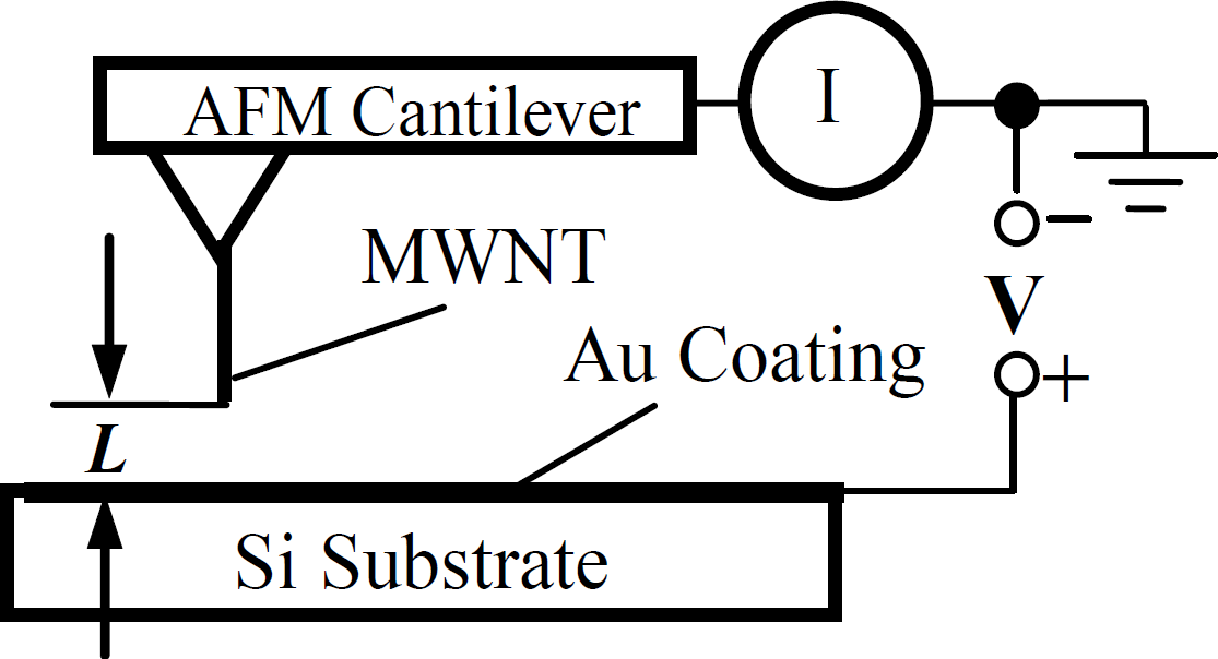
Design of a Mass Flow Sensor

A Mass Flow Sensor
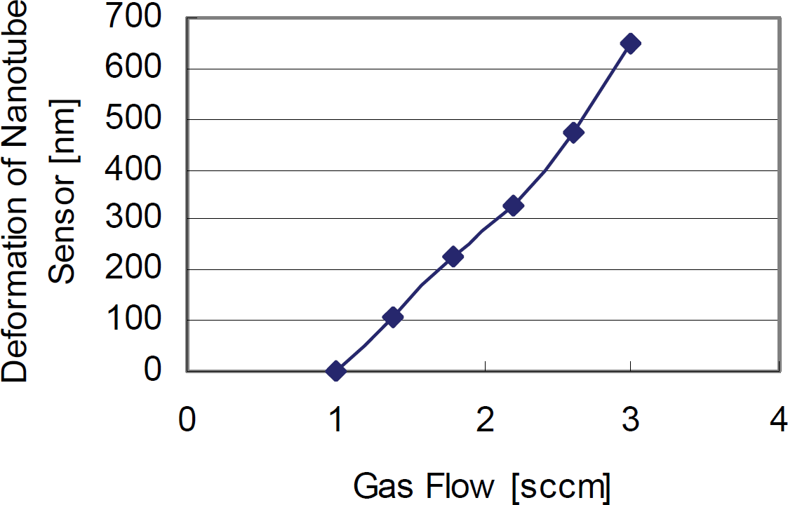
Calibration of Nanotube Mass Flow Sensor
Carbon nanotubes, with their nanometer diameters, up to 10–1000 aspect-ratios, TPa-order Young's modulus, extremely low turn-on fields and high current densities, have been rapidly recognized as one of the most promising electron field emitters ever since the first emission experiments reported in 1995. Property characterization and application of single nanotube emitters show a family of novel nanodevices.
Nanometer-sized sensors that can detect nanometer-scale distances in real time are highly expected. By using a cantilevered individual nanotube as an emitter, the relation between the field emission current and the distance between the tip and a substrate (as anode) has been investigated. When the CNT emitter approaches to the substrate, the emission current changes obviously. By detecting the change of the current, the distance can be understood. Based on this principle, it can be used as an approaching sensor.
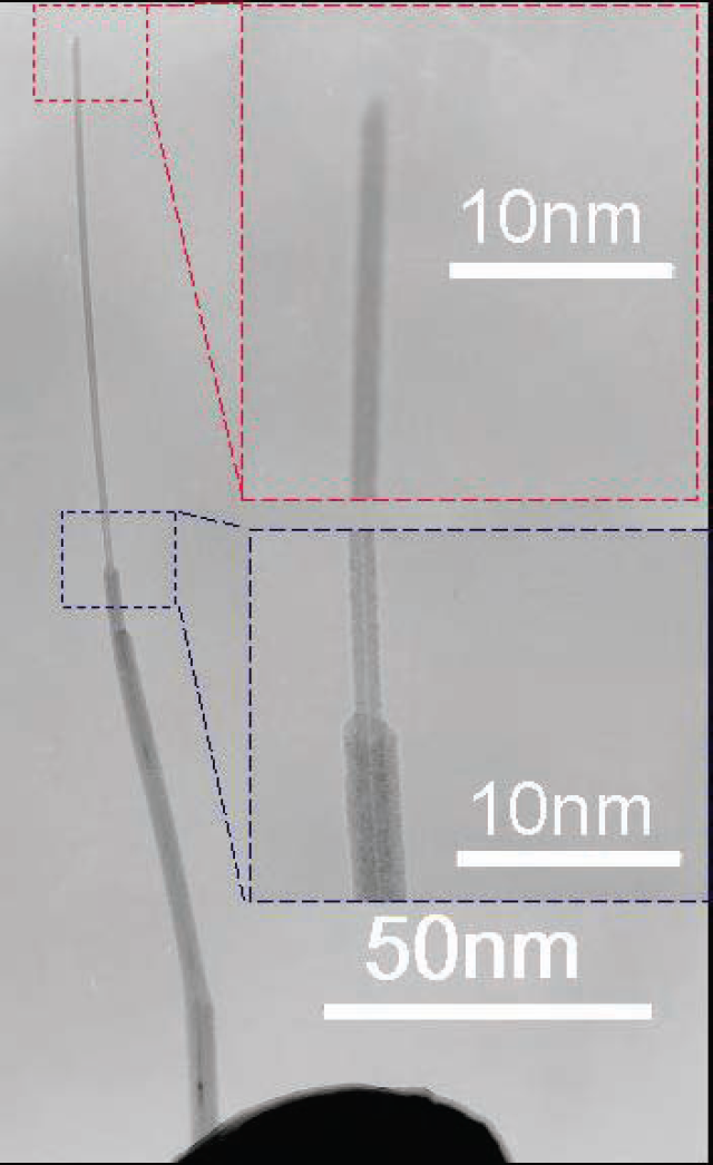
Fig. 8 shows an example (Arai et al., 2004a). The CNT is soldered on an AFM cantilever with EBID by introducing W(CO)6 as precursors. The CNT emitter is 15 nm in diameter and 2.26 μm in length. Using this CNT emitter as cathode, currents change as shown in Fig. 9 at different gaps under 150 V bias. For example, the current is 75 pA as the gap is 100 nm, and is 24 pA as the gap is 800 nm. When the gap is lager than 900 nm, the field emission current stopped. No degradation of the emitter is found during the experiment. A resolution around 100 nm was available and 10 nm is expectable.

Field-emission-based approaching sensor

Relation of gap between emitter tip and cathode and emission current under constant bias (150V)
The detection of the distance can also be based on the change of on-set voltage. Because the independence of the sensor on the microscope imaging, it can be not only used as independent approaching sensors, but as the sensing elements for deflection-based fg mass sensors, mass flow sensors and pN force sensors as well.
Through destructive fabrications, typically, a layered structure and a sharpened structure can be obtained (Dong et al., 2001c). As shown in Fig. 10 (a), a MWNT is supported between a substrate (left end) and an AFM cantilever (right end), which are in turn fixed on the Units 1 and 2 of the manipulation system. Fig. 10 (b) shows a zoomed up image of the central blocked part of Fig. 10 (a), and the inset in it shows its structure schematically.

Nanotube Linear Bearing
It can be found that the nanotube has a thinner neck (part B in Fig. 10 (b)) that was formed by destructive fabrication, i.e., by moving the cantilever to the right. To move it more in the same direction, a motion like a linear bearing is observed as shown in Fig. 10 (c), and it is shown schematically by the inset.
By comparing Fig.10 (b) and (c), we can find that part B remained unchanged in its length and diameter, while its two ends brought out two new parts I and II from parts A and B, respectively. Part II seems have uniform diameter (φ 22nm), while part I is a tapered structure with the smallest diameter φ 25nm. The interlayer friction has been predicted very small (Cumings & Zettl, 2000), but the direct measurement of the friction remains a challenging problem.
Telescoping structures (see Fig. 11) obtained from MWNTs have invoked many interests because of the possibility to be applied into nano mechanical systems such as nanometer scale actuators, ultra-low friction bearings, GHz nanooscillators, etc. Opened structures of CNTs have been initiated by removing the commonly capped ends, which seal in all inner-core nanotube cylinders, of as-grown MWNTs with acid etching, saturated current, electric pulse, or mechanical strain (Fig. 11) (Fukuda et al., 2003).
Telescoping MWNT
In situ manipulation of the nanotube core allows controlled reversible telescoping to be achieved and the associated forces to be quantified. Robust ultralow-friction linear nanobearings (Fukuda et al., 2003), rotary nanoactuators have been demonstrated on the bases of the interlayer motions (Fennimore et al., 2003).
Experiments show the field emission current from a telescoping MWNT (Fig. 12) can have a fluctuation with large magnitude as shown in Fig. 13. The “kink”-like local change of emission current has been argued to be caused by the motion of core nanotube, and the displacement can be detected from the magnitude (Dong et al., 2004). This suggests the device shown in Fig. 12 can be potentially applied as a linear actuator with field emission current serving as position feed back.

Field emission from a telescoping nanotube

A typical I-V curve of a telescoping nanotube as the inter-electrode gap G =500 nm
Nanotube scissors are designed for probing the conductivity or cutting a nanotube between the two arms with saturated current. A new design by applying conductive EBID deposits is shown in Fig. 14. To improve the cutting accuracy, it is necessary to modify the opening between the two arms (g). The key technique is the shape modification of nanotubes. Fig. 15 shows nanotube scissors fabricated by assembling two tubes on a commercially available AFM cantilever. Before shape modification, the opening between the two arms is larger than 1μm, whereas it is 85.6nm after modification.

Nanotube Scissors

Nanotube Scissors (Scale bars: 1μm)
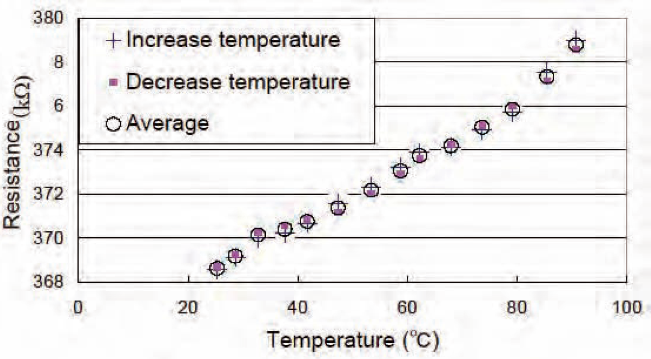
Dual nanotubes crossly cantilevered to two independent electrodes can be used as thermal probes. Fig. 16 shows a SEM image of AFM cantilever-electrode-based CNT thermal probes. Two single CNTs are fixed on the top and bottom sides of an AFM cantilever to form a set of thermal probes. The lengths of the CNTs are about 2 μm to 3 μm with 30 nm in diameters.

CNT thermal probes.
Fig. 17 shows the temperature-resistance relations. The resistances of the CNT thermal probes were measured in steps of 3–6°C. The results are averaged (circle) from similar measurement obtained during heating (+) and cooling (square). Ultra-small temperature scanning has shown the effectiveness and high sensitivities of the probes (Arai et al., 2004b).
Temperature v.s. resistance relation
Based on a robotic manipulation system, a nano laboratory—a prototype nano manufacturing system has been presented, which is composed with a nanorobotic manipulation system with 4 units and 16 DOFs, a nano fabrication system based on EBID with an internal or external precursor evaporation reservoir equipped with a thermal field emission electron source or a nanotube cold cathode, and a real-time observation and measurement system based on FESEM equipped with 3–4 conventional AFM cantilevers, piezoresistive levers or nanotube probes.
The state of the art of nanotube sensors and nanotube actuators are overviewed according to the number of nanotubes involved, configuration of nanotubes adopted, and physical properties/effects applied by focusing on our recent efforts on this exciting field. Field emission of a cantilevered nanotube based approaching sensors, resistance variation of cantilevered dual nanotube based thermal probes, and a potential telescoping nanotube linear actuator are reviewed in this report.
A new family of sensors and actuators, nano sensors and actuators, will be enabled if new materials and physical effects are discovered and new fabrication, assembly, integration and packaging technologies are developed.
Footnotes
Acknowledgments
This work was supported by JSPS.KAKENHI (15360136). The authors are grateful to Prof. Y. Saito at Nagoya University for providing us with MWNTs.