
Abstract
This paper presents a method of particle manipulation by dielectrophoresis (DEP) and immobilization using photo-crosslinkable resin inside microfluidic devices. High speed particle manipulation, including patterning and concentration control by DEP was demonstrated. Immovable and movable microstructures embedding particles were fabricated on-chip. Several microelectrodes were fabricated using Indium Tin Oxides (ITO) and Cr/Au. The two kinds of DEP responses of yeast cells (W303) and other particles were experimentally confirmed. Based on negative DEP phenomenon, cell traps generated by microelectrodes were demonstrated. Position control, transportation and patterning of cells were performed with cell traps. The on-chip fabrication of arbitrary shapes of microstructures based on Poly(ethylene glycol) diacrylate (PEGDA) was reported. With cell patterning by DEP and immobilization using on-chip fabrication, microstructures embedding line patterned cells were fabricated inside microfluidic channels. A novel microfluidic device was designed to separate patterning and fabrication areas and movable microstructures embedding concentration controllable particles were fabricated inside this device.
1. Introduction
Currently the research about high-throughput cell assembly is taken very seriously, since it can provide effective approaches for the construction of implantable in vitro artificial tissue for tissue engineering [1]. The cells inside real tissues and organs are arranged according to certain patterns and shapes, such as neural cells with line patterns, skin with reticular patterns and blood vessels with tube shapes [2]. To build artificial tissues, an important issue is how to form different patterns of cells as they are really arranged and how to immobilize these patterned cells inside certain structures for encapsulation [3, 4]. Moreover, the long-term co-culture of these patterned and immobilized cells is the key to constructing functional artificial tissues [5].
For patterning, existing methods include surface adhesion, optical tweezes and dielectrophoresis. By using surface adhesion as in reference [6], it is possible to manipulate cells without causing damage. However, the positioning is not flexible since surface adhesion depends on surface property which is not easily changed. Optical tweezers is a low-damage and easily controllable method. An automatic cell manipulation system has been constructed. However, the manipulation force is weak compared with flow resistance, as in [7]. Compared with other methods of cell manipulation, dielectrophoresis (DEP) is easier to control and it is non-contact which means there is less damage to cells [8]. Due to the low physiological stress caused by DEP, the cells remain viable after treatment and can be cultured for further purposes. As in reference [9], using DEP force, it is possible to manipulate particles with great selectivity. It is possible to allow the separation of cells or the orientation and manipulation of nanoparticles and nanowires. Furthermore, certain cell sheets with multilayers are constructed by DEP. As seen in [10], cells aggregate and adhere to each other based on the DEP. Patterned liver cell structures are also formed by DEP traps [11]. Consequently, DEP is widely used in cell manipulation, such as sorting, aggregation and patterning.
For immobilization, the convenient approaches are based on methods such as aspiration, solution pressure and fluidic structure, as in [12]. The advantage of aspiration and pressure is the large fixing force, while the disadvantage is the damage to the cells [13]. Using special fluidic structures, see [14], cells are immobilized inside microfluidic devices. However, the immobilized cells are difficult to analyze further. On-chip fabrication based on photo-crosslinkable resin via UV illumination as seen in [15] is a creative way of immobilizing cells. Cells are directly immobilized inside the photo-crosslinkable solution [16]. There are several advantages such as high-speed, low-cost and arbitrary shape [17].
We present a method of manipulating particles and cells by DEP and immobilizing them using photo-crosslinkable resin inside microfluidic devices. The whole research approach is shown in Figure 1. The key idea is to create cell structures by combining patterning and immobilizing methods. There are 3 advantages to this research. First, the non-contact cell patterning method based on DEP is high speed and low-damage. Second, the arbitrarily shaped microstructure can be effectively fabricated on-chip inside microfluidic devices. Third, the patterned particles and cells are easily immobilized inside microstructures and can be further assembled into complex three dimensional (3D) structures.
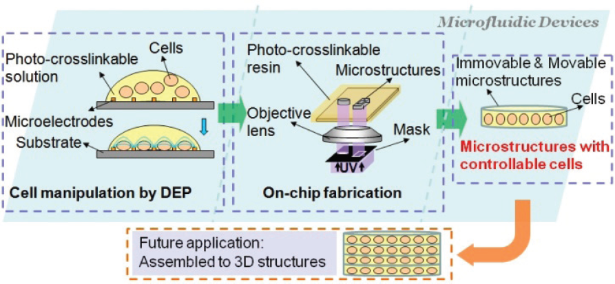
A schematic drawing of the cell assembly method
Cell patterning was conducted using dielectrophoretic microelectrodes which were fabricated by Indium Tin Oxides (ITO) and Cr/Au. We chose yeast cells (W303) and microbeads (polymer microspheres, Thermo Scientific) to use in the experiments as samples for demonstration purposes only. Line and circle patterns of cells and microbeads were constructed at a high speed. Cell immobilization was carried out using the on-chip fabrication method. Using the microscope, the patterned UV-ray was illuminated through the mask onto the photo-crosslinkable resin which was injected into the microfluidic device made of Polydimethylsiloxane (PDMS). The photo-crosslinkable resin, which is Poly(ethylene glycol) diacrylate (PEGDA), has a low toxicity [18]. Furthermore, cell viability is positively confirmed inside several kinds of PEGDA such as molecular weight 700 and 3400 [19]. The resin was polymerized and microstructures with arbitrary shapes are directly fabricated at desired places inside the channels of microfluidic devices.
As for related works, cell patterning using optical tweezers and immobilization by PEGDA has been carried out, as seen in [20]. However, the size of the cell embedded structures is limited because the UV and the laser use the same light path. Cell embedded PEGDA structures are fabricated in [21] while these cells are without control and patterning. There are cell embedded PEGDA structures patterned by DEP as seen in [22]. This approach includes some open chamber manipulation which is subject to contamination. Unlike embedded cases, cell structures can also be formed based on PEGDA structures, such as PEGDA micro wells [23, 24]. There is no scaffold for cells, which means that it is difficult to construct complex structures containing different kinds of cells. By using our method, on the other hand, movable microstructures embedding controllable cells can be directly fabricated inside microfluidic channels.
In our previous works, immovable microstructures embedding particles were fabricated on-chip as seen in [25]. In this paper, we improved upon the previous method and then fabricated the movable microstructures embedding particles and cells on-chip. In order to control particle concentration inside microstructures, a microfluidic device with separated patterning and fabrication areas was fabricated. Concentration control for embedded particles inside movable microstructures was demonstrated. These movable microstructures can be further assembled into more complex 3D structures and could become functional components of artificial tissue.
2. Cell traps based on dielectrophoretic microfluidic devices
2.1 Dielectrophoresis (DEP)
DEP is a phenomenon whereby a force is exerted on a dielectric particle when it is inside a non-uniform electric field. This force does not require the particle to be charged. All particles exhibit dielectrophoretic activity in the presence of electric fields. However, the strength of the force depends strongly on the electrical properties of the medium and the particles, on the shape and size of the particles, and on the frequency of the electric field, as seen in [26]. There are two DEP responses: p-DEP and n-DEP.
For a spherical particle of radius r suspended in a medium of permittivity εm, the dielectrophoretic force is given by the expression:

where Erms is the root mean square value of the electric field. Re[fCM] represents a real part of the fCM, which can be represented as follows:

where ε* is the complex permittivity which is calculated by ε* = ε – jσ / ω, then σ is the conductivity and ω is the frequency of the electric field. Subscripts p and m represent particle and the medium, respectively. Therefore, Re[fCM] > 0 means that the particle shows p-DEP responses so that the particle moves towards the part of the electric field with higher intensity, while Re[fCM] < 0 represents n-DEP response and the particle moves towards the part of the electric field with lower intensity [27].
2.2 Fabrication of ITO and Cr/Au microelectrodes and PDMS microfluidic devices
We developed special microelectrodes of which the size was approximately the same order as the cells. Microelectrodes are key elements in micromanipulation using DEP. Firstly, we chose ITO as a conductive material because it is transparent. The glass was coated with thin ITO and was used to fabricate microelectrodes. The thickness of the ITO layer is 150 nm. The fabrication method was based on photolithography. The photoresist AZ (5214-E, Clariant (Japan) K.K.) was used as the protective layer. The ITO microelectrodes are shown in Figure 2(a).

Fabricated ITO and Cr/Au microelectrodes
However, because the chemical etching is not easy to control, it is different to fabricate ITO microelectrodes of a precise size to within 10 μm. Besides, the resistance of ITO is not low enough to obtain a higher DEP force. We improved the microelectrodes and fabricated Cr/Au microelectrodes. The method of fabrication was also based on photolithography, while here the photoresist AZ (5214-E) worked as the sacrificial layer. The Cr/Au microelectrodes are shown in Figure 2(b). The width of the smallest electrodes is 4μm. It is much smaller than the ITO microelectrodes. Besides, the edge of the microelectrodes is very sharp and clear so that it is very suitable for precise and high speed micromanipulation of particles using DEP.
DEP force should be generated inside the solution which means the microfluidic channel is also needed. Microfluidic devices made of PDMS are key components in many microfluidic applications [28]. The mould of the microfluidic channel was made with photoresist SU-8 (MicroChem Corp.). The SU-8 mould was covered with PDMS (SILPOT 184 W/C, Dow Corning Toray) liquid and cured after 24 hours. After the PDMS was detached from the mould and used to cover the glass, holes were made at the ends of the channel. The silicone tube was put in the hole and the solution was injected into the channel using negative pressure.
2.3 DEP responses of yeast cell and Cell traps generated by negative DEP
There are two DEP responses of particles: p-DEP and n-DEP. Alternating Current (AC) and NaCl water solution were used to generate DEP force. By adjusting the frequency of the AC and the concentration of the NaCl solution (medium conductivity), these two DEP responses were generated. The reasons for using AC are as follows. First, operating at high frequencies eliminates any electrophoretic movement of the cell. Second, it is possible to eliminate electrochemical reactions at the electrode-electrolyte interfaces, preventing electrode corrosion and gas formation [29].
We confirmed the DEP responses of different particles such as polymer microspheres (Thermo Scientific), yeast cells (W303) and human umbilical vein endothelial cells (HUVECs) experimentally. We chose yeast cells and microspheres in the following experiments as samples for testing the functions of our system. In order to confirm the precise experimental parameters of p-DEP and n-DEP for yeast cells, an experiment was performed. To generate p-DEP, the concentration of the NaCl solution was 90 mg/L and the frequency of the AC was 1 kHz. To generate the n-DEP, the concentration of the NaCl solution was 200 mg/L and the frequency of AC was 500 kHz. In both cases the Vpp of the AC was 8 V.
n-DEP is often used for manipulating particles. For example, in [30], special structures of electrodes are applied to trapping cells at desired positions based on n-DEP. One kind of cell trap was designed and numerically simulated, as shown in Figure 3. The black parts are the ITO electrodes and there are several holes inside the large ones. The edges of the electrodes should be the areas of the highest intensity of the electric field, so the centres of the holes should be the lowest areas. Due to the n-DEP, particles move towards the part of the electric field with lower intensity which means the particles will be trapped inside the holes. So these holes are called cell traps. The simulation results from the electric field show the positions of lowest intensity of the electric field are the centres of the holes. The particles inside this electric field will move to the holes and be trapped when n-DEP is generated. It is possible to use this structure to trap and control the position of particles.

The model of microelectrodes and numerical simulation of electric field distribution at the cross section A-A'
The fabrication procedure of this microelectrode is mentioned in section 2.2. With the parameters for the generation of n-DEP, the experiment of trapping yeast cells was conducted. One line of 5 yeast cells was formed. As shown in Figure 4, yeast cells were trapped inside the holes of which the diameter was about 10 μm.

One line of 5 cell traps and trapped yeast cells
3. High speed micromanipulation of particles and cells using DEP cell traps
3.1 Position control and transportation of yeast cells
Using the fabricated cell traps, the position control and transportation of the yeast cells was performed inside the microfluidic device. The concentration of the NaCl solution used was 200 mg/L, the frequency of the AC was 500 kHz and the Vpp of the AC was 8 V. As shown in Figure 5, firstly, a yeast cell was trapped in the left cell trap while the AC was being turned on. Secondly, the cell moves to the middle cell trap while AC was being turned off. Thirdly, the cell was trapped in the middle cell trap once the AC was turned on again. The solution flow inside the channel went in a right-hand direction. By adjusting the flow velocity, it was possible to control the position and movement velocity of the cells flexibly. In Figure 5, the time cost for cell position transportation from middle to right is 5 seconds shorter than from left to middle because of the increase of flow velocity. The AC supply and flow velocity can be controlled by peripheral equipment.

Control and change the position of yeast cell by DEP traps and liquid flow inside microfluidic chip. (a), (c) and (f) are positioning state of target cell. (d), (b) and (e) are transportation state of target cell.
The trapping force is calculated based on the resistance force of the cells given by the liquid flow. After one cell is trapped inside the hole, the flow velocity is increased continually. At the moment the cell escapes from the trap, the trapping force is equal to the resistance force which is calculated by the following expression:

where e˜ is the viscosity of solution, v is the velocity of solution and r is the radius of the cell. Therefore, the trapping force for this experiment was about 6 pN.
3.2 High speed patterning of particles
A cell trap matrix made of several lines of electrodes was fabricated, as shown in Figure 2(a). The size of the trap and the electrode is about 11 μm and 30 μm, which is suitable for the size of a yeast cell. With this novel microelectrode, high speed patterning of yeast cells was demonstrated, as shown in Figure 6(a). The patterning of hundreds of yeast cells was completed within 1 second and the pattern was automatically formed. It shows the potential application of this procedure in high-speed cell manipulation for tissue engineering.

The high speed patterning of cells and particles
Two kinds of Cr/Au microelectrodes were also fabricated and particle manipulation was performed. One of these microelectrodes is shown in Figure 2(b). The concentration of the NaCl solution used was 200 mg/L, the frequency of the AC was 500 kHz and the Vpp of the AC was 8 V. Microbeads with 7 μm diameter were used (microsphere, catalogue number 4207A, Thermo Scientific). The experiment results are shown in Figure 6. Figure 6(b) shows the line pattern generation of microbeads. Figure 6(c) shows that the microbeads were manipulated using concentric circle patterned microelectrodes and 5 beads were trapped and then formed a partial circle pattern (highlighted in blue). By controlling the flow velocity and the AC, it is possible to manipulate particles continuously.
4. On-chip fabrication of arbitrary microstructures
4.1 Equipment of on-chip fabrication system
The method for the on-chip fabrication of arbitrarily shaped microstructures is shown in Figure 7. An optical microscope (IX-71, Olympus) was used to observe samples and expose samples to UV. X-Y stage and height of the objective lens (Z-axis) were controlled in order to adjust fabrication positions. Several objective lens were used, including oil immersion objective UPLFLN 100XOI2, 60X and 40X (Olympus). UV was shone using the mercury lamp (USH-103tems) and controlled by the shutter (BSH-RIX, Sigmakoki). The microfluidic device was put on the stage. The observation was performed using a CCD camera (XC-555, Sony).
4.2 On-chip fabrication of arbitrary microstructures and movable microstructures embedding cells
As shown in Figure 7, the mask made of PET (polyethylene terephthalate) was set in front of the shutter on the optical axis. The patterns on the mask can be arbitrarily shaped based on the design. UV was shone through the mask from bottom of the objective lens onto the PEGDAs (Sigma Aldrich, molecular weight 200, 700) inside the channel of the PDMS microfluidic device. Then the PEGDAs were polymerized using the patterned UV and the arbitrarily shaped microstructures were fabricated inside the channel [31].

A schematic drawing of the method of on-chip fabrication and images of fabricated microstructures
The position of the fabricated microstructure was confirmed by the stage. It is possible to fabricate microstructures at any desired positions. As mentioned in [32], when the surface of the bottom of the channel is glass, the fabricated microstructure adheres to the glass surface. When the surface of the channel bottom is PDMS, the fabricated microstructure is able to move in the non-polymerized resin freely without adhering.
The fabricated microstructures are shown in Figure 7. They were fabricated by shining the UV-ray for 0.2 seconds using the objective lens of 100X and 40X. With different masks, different microstructures with large amounts can be fabricated in a short amount of time [31]. Furthermore, by programming control software for the UV lump shutter and the stage of the microscope, it is possible to carry out automatic on-chip fabrication.
A solution mixed with yeast cells and PEGDA was prepared and then injected into the microfluidic channel. This channel has a PDMS coated bottom surface.
Movable microstructures embedding cells were directly fabricated inside the microfluidic channel as shown in Figure 8. However, here the embedded cells were randomly distributed and uncontrollable.

Fabricated movable microstructure embedding cells
5. On-chip fabrication of immovable microstructure embedding patterned cells
5.1 Combination of ITO microelectrodes and on-chip fabrication
Based on the cell patterning method using ITO microelectrodes and the on-chip fabrication method, the fabrication of immovable microstructures embedding patterned yeast cells was conducted first.
The experimental setup is as follows. First, the ITO microelectrode shown in Figure 2(a) and the PDMS microfluidic device were prepared. The ITO microelectrode was covered with a PDMS chip and formed a microfluidic channel. Second, a solution containing 30% PEGDA (molecular weight 700) and 200 mg/L NaCl was prepared. The reason why we used PEGDA (700) is that it can dissolve in water. Then the yeast cells (W303) were mixed into the solution. Third, the solution was injected into the microfluidic channel. An AC power supply was used to generate DEP force. The frequency of the AC was 500 kHz, and the Vpp of the AC was 8 V. Fourth, after the cell pattern was formed, the objective lens was adjusted to the patterning position. Then UV was exposed for 0.2 seconds to fabricate the microstructures at the same position as the patterned cells. The whole procedure is shown in Figure 9.

Fabrication procedure of Cr/Au microelectrode
5.2 Immovable microstructure embedding patterned cells
Donut-shaped masks were used. Therefore, after the line patterns of yeast cells were formed, donut-shaped microstructures were fabricated at the same position. Here we found that the DEP response of cells changed to p-DEP and the reason was that the conductivity of the solution used changed compared with the previous one which is only NaCl solution. This microstructure contains 3 lines of yeast cells, as shown in Figure 10. For Figure 10(b), the inner and outer diameter of the donut shapes is 35 μm and 100 μm respectively. There are approximately 100 yeast cells inside this microstructure. In figure 10(d), which is cleaned by a flowing solution without cells, only the immobilized cells remain clearly inside the microstructure.

The images of immovable microstructures embedding patterned cells.
In the microstructures, yeast cells were formed into a pattern of 3 lines. The pattern was generated in about 10 seconds and the microstructures were fabricated in 0.2 seconds. This high speed fabrication is easily controlled and the cells are automatically patterned. Therefore, it is possible to fabricate this kind of microstructure very quickly and immobilize large amounts of cells inside them. However, the fabricated microstructures are immovable which means it is difficult to manipulate and assemble them in order to form larger 3D structures.
6. Cell concentration control for movable microstructure embedding particles
6.1 Microfluidic chip with separated patterning and fabrication areas
The cells inside the movable microstructures of section 4.2 are randomly distributed and uncontrollable and the fabricated microstructures of section 5.2 are immovable. However, it is important to control the cell concentration inside certain areas for in vitro culture. It is also important to make cell embedded microstructures manipulable so they can be functional components in the construction of artificial tissues. Therefore, a microfluidic device was designed to control cell concentration inside on-chip fabricated movable microstructures. As shown in Figure 11, there are separated patterning and fabrication areas in this device and 3 groups of Cr/Au microelectrodes. The electrodes of Group 1 are able to stop the particles inside the channel, acting as a “Switch”. Group 2 concentrates particles to the PDMS coated fabrication area. Group 3 separates the microstructures and particles after fabrication. Patterned UV will expose the fabrication area only. The width of the microelectrodes and the gap is 20 μm. In the following experiments, the frequency of the AC used was 500 kHz and the Vpp of the AC was 8 V.

Microfluidic chip with separated patterning and fabrication areas
With these two groups of microelectrodes, it is possible to obtain movable microstructures with different concentrations of cells or particles after UV exposure.
6.2 Experimental results of controlling the concentration of embedded particles
Figure 12 shows the experimental results of concentrating microbeads in the centre of the channel, forming a long line. The solution used is 200 mg/L NaCl water solution mixed with 7 μm microbeads (catalogue number 4207A, Thermo Scientific). By controlling group 1 and 2 electrodes, the beads were stopped (Figure 12(b), 12(c)) and concentrated in one line (Figure 12(c), 12(d)).

Experimental results of controlling the cell concentration
Figure 13 shows the fabricated microstructures with different numbers of microbeads. A 30% PEGDA (molecular weight 700) and 200 mg/L NaCl water solution mixed with 10 μm microbeads (catalogue number 4210A, Thermo Scientific) was used. There are microstructures containing one to six microbeads. The manipulation and concentration control of the particles was performed within 10 seconds, and the microstructures were fabricated in 0.2 second. This high speed fabrication and manipulation shows the great potential of this method for use in high-throughput cell manipulation and immobilization for tissue engineering. These movable microstructures can be further assembled to form much more complex 3D cell structures. With cell culture, these cell embedded microstructures could become functional components of artificial tissue.

Movable microstructures embedding microbeads of which the concentration (number) is controllable are fabricated in the microfluidic channel
7. Conclusion
We presented a new method of fabricating movable microstructures embedding controllable particles inside microfluidic devices. It was combined with micromanipulation using DEP and immobilization using photo-crosslinkable resin. Particle micromanipulation, including patterning position control and concentration control was demonstrated. Several microelectrodes were fabricated using ITO and Cr/Au. The two kinds of DEP responses of yeast cells (W303) and other particles were experimentally confirmed. Cell traps generated by microelectrodes were demonstrated. Position control and transportation of yeast cells was performed with cell traps. A cell trap matrix was fabricated and high speed cell pattering was performed. The on-chip fabrication of arbitrarily shaped microstructures based on PEGDAs was demonstrated. Immovable microstructures embedding 3 lines of yeast cells were fabricated in a dielectrophoretic microfluidic device, inside a PEGDA and NaCl solution. Furthermore, another novel dielectrophoretic microfluidic device with separated patterning and fabrication areas was proposed. Movable microstructures embedding microbeads of which the concentration (number) is controllable by microelectrodes were fabricated inside this device.
In future works, 3D and larger structures need to be assembled in order to apply the method to tissue engineering based on fabricated movable microstructures. The next issue is finding a method for the high speed assembly of these microstructures.
Footnotes
8. Acknowledgments
We wish to thank Prof. Toshifumi Inada at Tohoku University for providing us with the yeast wild-type strain W303. This work was partially supported by MEXT KAKENHI (Hyper Bio Assembler for 3D Cellular Systems (BioAssembler)) and Nagoya University Grobal COE Program (COE for Education and Research of Micro-Nano Mechatronics).