
Abstract
Flapping-wing robotic insects are novel micro air vehicles (MAVs) inspired from biological insects in order to achieve a small size, high manoeuvrability and super remote ability. Such MAVs are centimetre scale flying robots with a number of applications, including exploration, environmental monitoring, rescue and reconnaissance. Due to the strict weight and power requirements of MAVs, the power electronics topologies need to be considered seriously. This paper describes state of the art power electronics topologies suitable for driving fl This -wing robotic insects. Comparisons are made in the resulting configurations of MAVs across several key metrics to estimate their performance. Discussion on the effect of performance gains in various power electronic topologies are abridged and presented.
1. Introduction
The latest research shows that insects were the first animals to evolve active flight and remain unsurpassed in many aspects of aerodynamic performance and manoeuvrability[1]. Bionic flapping-wing robotic insects are a class of new conceptual air vehicles that take design cues from flying modes of insects in order to achieve a pretty small size, high manoeuvrability and strong hovering ability[2][3]. Several implemented prototypes of flapping-wing robotic insects have shown good prospects, including the Micromechanical Flying Insect and the Harvard Microrobotic Fly which pioneered in robotic insects capable of lifting off with external power[5].
Remarkable progress has been made with respect to designing and optimizing the individual subsystems of flapping-wing robotic insects, including aerodynamic component[6], actuation[7], power electronics[8] and fabrication options[9]. One of the critical challenges in MAVs' design is the selection of actuation scheme that can provide sufficient power for autonomous flpowe. When the required characteristic dimensions of MAVs fall below 10cm, traditional actuators, such as electromagnetic motors, have a considerable disadvantage in efficiency and power density due to an increased dominance of surface effects[10]. Plenty of alternative methods, such as piezoelectric[2] and thermal[11] actuators, have been proposed for flapping-wing robotic insects.
Compact energy sources suitable for flapping-wing robotic insect applications, such as lithium batteries, supercapacitors[12] solar cells[13] as well as fuel cells[14], all generate output voltages below 5V. In addition to various kinds of mechanical performances, the above mentioned actuation techniques have diverse electrical requirements, including wide variations in driving voltages and currents[15]. Therefore, MAV actuator selection and power electronic interface design are the most critical aspects for MAV design.
In this paper, plenty of MAVs with excellent size and flight actuation principles comparable to dipteran insects are summarized based on current and previous research. In addition, some promising power electronics topologies are described. Those topologies which generate high, time-varying voltages necessary for the operation of actuators, fulfil the stringent weight requirements of microrobotic systems and optimize the system efficiency.
2. State of the Art MAVs
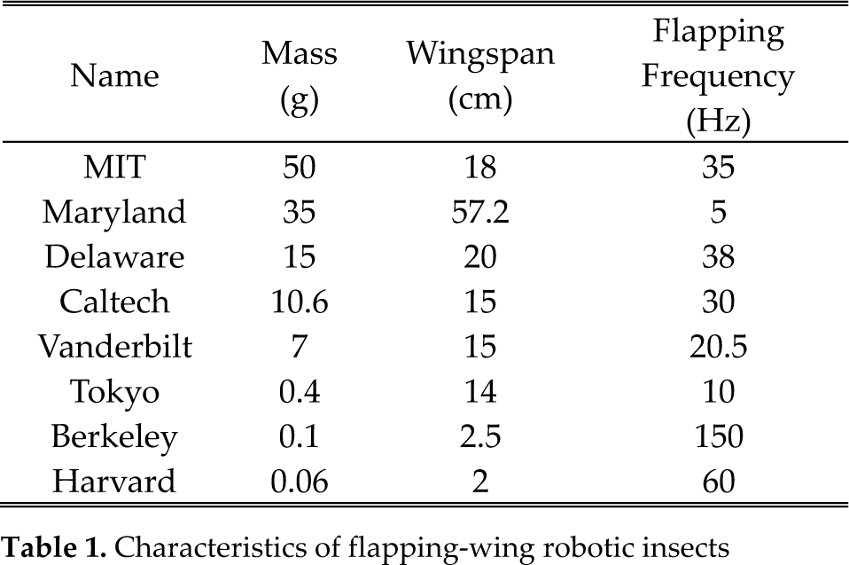
In the past decade, researchers achieved remarkable progress in MAVs' design. The first MAV was fabricated at MIT. With the name ‘Entomopter’, this MAV utilized reciprocating chemical muscles to power the 50g flapping-wing device. The Entomopter has an 18cm wing span and wing flapping occurs at a 35Hz constant frequency[16]. A group in mechanical engineering at the University of Maryland worked on bird-inspired robotics research. They demonstrated that a flapping-wing MAV with folding wings is able to fly at reduced forward velocity[17]. The main features of the bird are presented as follows: 35g low overall weight, 57.2cm wingspan and 5Hz flapping frequency. Meanwhile, a team at the University of Delaware constructed a small ornithopter using rotary and parallel mechanisms called Microbats, which have a 20cm wingspan, sub-15g weight and a 38Hz flapping frequency[18][19]. On a similar scale, researchers from Caltech and Aerovironment created an RC flapping-wing MAV based on novel MEMS wing technology to fabricate a wingframe using titanium-alloy metal called the ‘Microbat’[20][21]. The best free flight durations of 9 and 18 seconds were achieved by super capacitor powered and battery powered ornithopters, respectively. The design specifications are summarized as follows: with a total mass of 10.6g, 15cm wingspan, structure in resonance at 30Hz[22]. Piezoelectric actuators were also used as part of a tuned resonant drive for another two-wing MAV by a group at Vanderbilt University [23]. Specifically, this group utilized three piezoelectrically actuated flexure-based mechanisms that transform the linear output of piezoelectric unimorph actuators into a single-degree-of-freedom flapping motion. The design specifications are summarized as follows: with a total mass of 7g, 15cm wingspan, structure in resonance at 20.5Hz. Researchers at the University of Tokyo have mimicked butterfly flight using a robot with the following specifications: mass 0.4g, 14cm wingspan at 10Hz flapping frequency [24]. Researchers at U.C. Berkeley made a tremendous breakthrough in generating biologically-inspired wing trajectories using parallel mechanisms and miniature piezoelectric PZN-PT unimorph actuators[25][26][27]. The design specifications are summarized as follows: 0.1g mass, 2.5cm wingspan, 150Hz wingbeat frequency. In addition to flapping-wing versions, there were a lot of attempts at creating centimetre-scale rotary-wing MAVs. One of the most ambitious ones was the microrobotic fly at Harvard[2][8]. The design specifications are summarized as follows: with a total mass of 0.06g, 2cm wingspan, 60Hz resonance frequency. The characteristics of the above flapping-wing robotic insects are shown in Table 1. Based on the above background introduction, MAVs are evolving to be ultra-small size, super-light and to have long flying distance. Thus, a big challenge in weight, size and power density is given to power electronics interface design.
Characteristics of flapping-wing robotic insects
3. Power Electronics
According to the differences in power sources and drive electronics, the actuation techniques mentioned earlier are classified into two categories. Thermal and shape memory actuators should be driven in current mode, which requires high currents and relatively low voltages. Electrostatic, piezoelectric, as well as dielectric elastomer actuators should be driven in voltage mode, which requires high voltages and low currents.
In the above mentioned models, a circuit interface with high power efficiency and density is required to transfer energy from power source to actuator. This interface usually consists of power stage and driving stage. The former aims to converts the battery voltage to some required level. The goal of the latter is to convert the output of the power stage into a time-varying signal across the input terminals of the actuator. This section presents potential solutions to this design problem for both current mode and voltage mode actuators.
3.1. Current Mode Actuator
These kinds of actuators are micromechanical devices that typically generate motion through thermal expansion amplification. A small amount of thermal expansion in one part of the device is converted to a large amount of deflection in the overall device. They rely on high injection currents to increase the temperature of the active material. This process is achieved internally by electrical resistive heating. In many applications, the drive signal delivered to the actuator may be lower than the voltage of the power source (battery).
Presented in the following papers, electro-thermal cantilever micro actuators are broadly used in electronic instruments such as MAVs, scanners, projectors and so on. In reference[28], a CMOS thermal actuator based on inverted-connected metal line in bimorph design was developed and characterized. The driving voltage for this thermal actuator is between 0V and 3V, where the test structure achieved a vertical displacement of 48μm at 3Vdc and calculated power of 139mW. Another electro-thermal cantilever micro actuator with large vertical motion at low voltage is presented in reference[29]. With 0.5V applied voltage, the electro-thermal actuator, which possesses a high quality cantilever and produces large vertical deflection, can generate a vertical displacement of 42.9 μm. Finally, thermal actuator-based micro tweezers with three different driving configurations were designed, fabricated and characterized in reference[30]. This illustrates the simulated tip displacement of all the micro tweezers with a 0V~1.2V applied voltage range. Above all, although there is little difference in driving voltage, they are between 0V and 3V.
Because the output voltage of a conventional buck converter (input voltage comes from single-cell lithium polymer battery with a nominal voltage of 3.7V) is too low to drive electro-thermal cantilever micro actuators. So the conventional boost converter becomes impractical in those cases. Two alternative techniques are presented to achieve low voltages in a compact package: a cascade buck converter[31] and a tapped inductor buck converter[32].
One of the feasible ways to convert the battery voltage to the expected value is to use an n-stage cascade connection of conventional converters with a single active switch. This makes it useful for tasks converting the 3.7 V typical battery voltage down to the few volts needed by the electro-thermal actuators. One of the major advantages of these converters is their high gain. However, a drawback is that the total efficiency may be low if the number of stages is high, since switching loss dominates the power losses. An interesting scheme is to have n-converters connected in cascade with single active switch. The required switching elements are: an active switch (Power MOSFET) and 2n-1 passive switches (diodes). This class of converters can be used only when the required number of stages is not very large. Otherwise the efficiency will deteriorate. The topology of an n-stage cascade buck converter is shown in figure 1.
Another feasible topology named a tapped inductor buck converter is presented in figure 2. From this figure we can see that the output voltage to drive thermal actuator is obtained from conversion of lithium polymer batteries' input voltage. This circuit utilizes a tapped inductor operated by one main switch to achieve high gain, with the square of turn ratio between the primary and secondary windings.
Some comparative evaluations of the available two topologies are shown in Table 2.
Some comparative evaluations of the available two topologies


N-stage cascade buck converter

Tapped inductor buck converter
Table 2 shows that a tapped inductor buck converter uses fewer components than an n-stage cascade buck converter, however, difficulties mainly lie in circuit fabrication, since a commercial tapped inductor is not available on the market at present. Furthermore, both feasible topologies have lower gain than the traditional buck converter. The latter one depends on the turn ratio. For a better understanding in the gain of the two different topologies, we use n=2 in an n-stage cascade buck converter and N=7 in a tapped inductor buck converter, the graph of the two topologies' gain is shown in figure 3 and the gain graph of the traditional buck converter is also illustrated.
Due to the strict power efficiency requirement of MAVs, the efficiency of those two circuits was simulated as shown in figure 4 using a hard switching operation. For the former circuit, the higher the output power, the higher the efficiency we can obtain where the increasing tendency of efficiency is subjected to exponential distributions, but total efficiency may be low depending on the number of stages. Actually, the efficiency can get nearly 70% under 0.5mW output power. For the latter topology with 85% maximum efficiency the average efficiency is higher than 82% which a nearly 3% improvement compared with a conventional buck converter.
3.2. Voltage mode piezoelectric actuators
The power electronics circuit must be capable of converting the low input voltage from fullriver lithium polymer batteries to a high output voltage, which works as the drive signal to power a piezoelectric actuator. The drive signal must be unipolar in order to achieve high deflection in the actuator without depolarizing the piezoelectric layers[7]. Such kinds of actuators require high voltages, nearly hundreds of volts, aiming at producing sufficient electrostatic forces or high electric fields. Unlike current mode actuators, where voltage gains are unlikely to exceed 10, voltage mode actuators may necessitate voltage gains of up to several hundred. Moreover, since only a part of the input electrical energy is converted by the actuator into mechanical output, it is highly desirable for the drive electronics to be capable of recovering unused energy from the actuator for use in subsequent actuation cycles.
Due to losses in the inductor and switching transistor, operating at a very high duty cycle, the conventional boost converter becomes impractical. Five alternative techniques are presented to achieve high voltages in a compact package: a voltage multiplier hybrid boost converter, a tapped inductor boost converter, a positive output cascade boost converter, a high conversion ratio boost converter and a power amplifier using a piezoelectric transformer[15].
A feasible hybrid voltage multiplier is a boost converter consisting of a classic boost converter circuit cascaded with a switched-capacitor charge pump circuit. It can be used to generate AC or pulse voltages ranging from a few volts for electronic appliances, to millions of volts for purposes such as high-energy physics experiments and lightning safety testing, the topology is shown in figure 5, which is a realized method to drive piezoelectric microrobots[10] and electrostatic MEMS devices[33].
Operating in a regime of high efficiency, the boost converter stage provides a moderate boost to the input voltage, while its pulsed output naturally charges up the capacitor ladder through the diodes. The charge pump multiplies the boost converter's output voltage. Ideally, the voltage gain equals the number of charge pump stages. Each additional stage of two diodes and two capacitors double the peak AC supply voltage. The maximum output power is limited by the size of the charge pump capacitors and the maximum output power of the boost converter.

Graph of three topologies' gain

Efficiency curves of two topologies
Figure 5 depicts the proposed topology. It is an n-levels DC-DC converter based on one switch, 2n+1 diodes and 2n capacitors. One advantage of the topology is that the number of levels can be extended by only adding capacitors and diodes, and the main circuit does not need to be modified.
The lowest part of the converter, figure 5, is the conventional DC-DC boost converter. Thus, the voltage gain equals the gain of a conventional boost converter. The difference between the hybrid voltage multiplier boost converter and the conventional one is that in the hybrid voltage multiplier, the output is Vo times n, where n is the converter's number of levels taking into account the zero level. This behaviour is achieved since the voltage multiplier in the boost converter's output is driven by the only switch in the converter.
Changing the inductor in the classic boost converter to a tapped inductor, as shown in figure 6, results in a combination of the boost and flyback voltage converter topologies[34]. As can be observed, the change from the traditional boost converter is not significant, but the boosting capability is increased considerably as it will be shown. Voltage gain is therefore determined by the switching duty cycle and the turn ratio of the transformer.
The voltage lift (VL) technique is widely used in electronic circuit design. It has been successfully employed in DC/DC converter applications in recent years and inspired the design of high voltage gain converters. Three-series Luo-converters[35–43] are examples of VL technique implementations. Their output voltage increases stage-by-stage along the arithmetic progression[40–42]. The super-lift technique increases the voltage transfer gain. Despite the high circuit complexity, positive output super-lift Luo-converters produce output voltage stage-by-stage along the geometric progression[35]. This section introduces positive output cascade boost converters that implement the output voltage increase in a simple geometric progression. It also effectively enhances the voltage transfer gain in power-law terms. To concentrate on the super-lift function, we need to focus on the two-stage boost circuit, which sufficiently satisfies the demand of driving piezoelectric actuators due to its high gain. The two-stage boost circuit is derived from the elementary boost converter by cascading. The circuit diagram is shown in figure 7.
Figure 8 shows the circuit configuration of high conversion ratio boost converter. It is used to transfer energy from the DC source Vin in the low voltage side to the DC source Vo in the high voltage side. When the proposed converter is operating in the boost mode, the circuit characteristic is cascaded by the boost converter and flyback converter with the voltage doubled [44] [45].
A piezoelectric transformer (PT) is characterized to be most feasible power convertor and has been widely used in actuators and sensors. The principle of operation is a combined function of actuators and sensors so that energy can be transformed through mechanical vibration [46]. The operation principle of PT is that the “primary” side of the PT excites mechanical oscillations in the piezoelectric material, while the “secondary” side generates a voltage. PT geometries suitable for step-up applications are described in[47].

Hybrid voltage multiplier boost converter

Tapped inductor boost convertor

Cascade boost converter
Generally, PT has to operate close to the mechanical resonance frequency in order to obtain high voltage gain and power efficiency. Its equivalent electrical circuit is shown in figure 9(a). The gain of a PT is pretty high under low loads, making it a good solution for the high voltage, low current voltage mode actuators [15].
Figure 9(b) shows the Class “E” resonant topology with fewer additional components than other power convertor topologies. The inductor is selected to resonate with the input capacitance Cin of the PT at a frequency close to the mechanical resonance frequency[48]. This topology transfers energy to PT from the inductor in the primary side when the switch is off. The switch is turned off again as soon as the voltage across Cin rings decline to zero[48]. Regulation of the output voltage is achieved by varying the switching frequency.
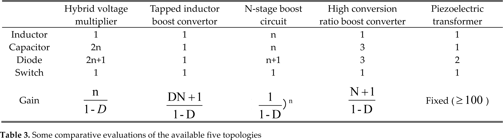
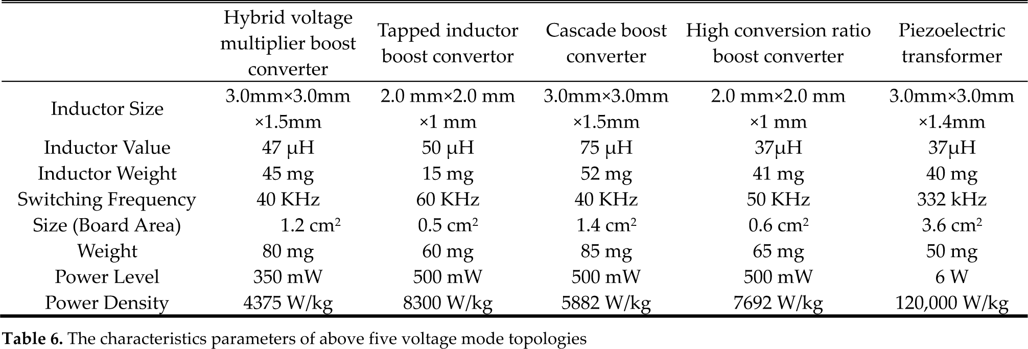
Some comparative evaluations of the available five topologies are shown in Table 3.
According to Table 3, a hybrid voltage multiplier boost converter has n times gain in contrast to a conventional boost converter, since it uses n times voltage multiplier. The disadvantage of this topology is its large size, high weight and low efficiency (caused by the multiplier). However, it is commonly used in hundreds of volts voltage output because it is easily fabricated. Since a tapped inductor boost converter can achieve the boosting capability without a high duty cycle, good efficiency is obtained. To achieve high voltage gains, this method has a much smaller parts number than the hybrid voltage multiplier boost converter. However, the rectifier diode and output capacitor must be rated for the output voltage. Additionally, a custom transformer may be required, since no commercial parts below 10g could be identified. As can be observed in Table 3, an n-stage cascade boost converter has a higher gain than the traditional boost converter. The gain also depends on the switching duty cycle. With this simple converter, a high boosting function can be obtained. As illustrated in Table 3, a high conversion ratio boost converter can get high voltage gain by increasing the turns ratio of the coupled-inductor. This converter has the same disadvantage as a tapped inductor boost converter, the customized transformer is a critical factor and hard to fabricate. Due to the simple geometries, a piezoelectric transformer is better than a magnetic transformer as it has potential in milligram-scale power actuator design.
Some comparative evaluations of the available five topologies

High conversion ratio boost converter

(a) Piezoelectric transformer equivalent circuit (b) Class “E” power amplifier topology
To get a better understanding in the performances of those five different topologies, we set n=3 in hybrid voltage multiplier boost converter, N=7 in tapped inductor boost converter, n=2 in cascade boost converter and N=7 in high conversion ratio boost converter. The graph of five topologies' gain is shown in figure 10.
Furthermore, we stimulated all five different topologies, the efficiency curves are shown in figure 11. With regard to a hybrid voltage multiplier, the higher the output power, the higher the efficiency we can obtain. However, the increasing tendency of efficiency is subjected to exponential distributions. Actually, the efficiency can reach nearly 55% under the 0.5mW output power. The tapped inductor boost convertor was optimized for 0.1-0.5 W output power. As a result, the peak efficiency occurring in this operating region is 72.3%. The n-stage boost circuit was optimized for 0.1-1 W output power. As a result, the peak efficiency occurring in this operating region is 90%. The high conversion ratio boost converter has the best efficiency of the total five different topologies. The maximum converter efficiency is about 94% and the efficiency at full load 0. 5W is 90.9%. The efficiency of the piezoelectric transformer is nearly 95%. Apparently, the overall efficiency of the piezoelectric transformer is better than other four different topologies with the same power supply specification as above.
3.3. Voltage mode dielectric actuators
Dielectric elastomers (DEs) are electrically actuated material devices which produce large deformation when a high driving voltage is applied to the electrode. Owing to their simple operating principle, dielectric elastomer actuators (DEAs) transform electric energy directly into mechanical deformation. DEAs which are light in weight have a high elastic energy density and have been investigated in many potential applications, such as robotics, power generation and sensing of force and pressure.
As presented in the following papers, DEAs are broadly used in electronic instruments in our daily life. In reference[49], a thin dielectric film is produced using fully automated fabrication which can offer the possibility MAV application. The drive voltage for this dielectric film is 600V, far below 1kV, where the corresponding typical dynamic deformation is 30μm. Another mm-size dielectric elastomer actuator chip on Pyrex is fabricated using low energy metal ion implantation[50]. This actuator is capable of out-of-plane displacement up to 250μm for 2mm diameter devices at 600V driving voltage. Finally, a conclusion was made about the 1KV driving voltages of dielectric elastomer actuators15].
Since voltage conversion from single-cell lithium polymer batteries to a voltage which can drive dielectric elastomer actuators is so high, the conventional boost converter becomes impractical in these cases. There is a feasible circuit which can achieve nearly 1KV voltage output with compact package[51]. The two-stage double boost converter is shown in figure 12 which is derived from the two-stage boost circuit by adding a Double/Enhance Circuit (DEC) in each stage circuit.
Some evaluations of a two-stage double boost converter are shown in Table 4.
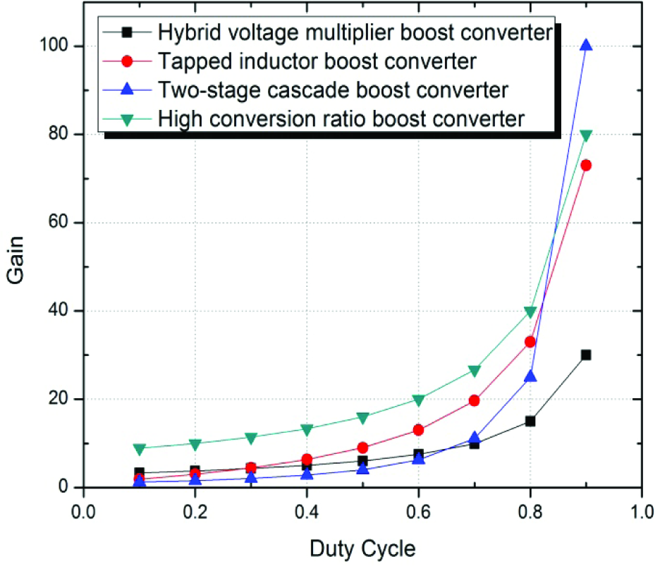
The graph of five topologies' gain

Efficiency curves of five topologies
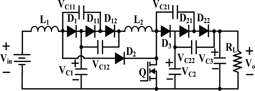
Two-stage double boost converter
Some evaluations of a two-stage double boost converter

The voltage gain of a two-stage double boost converter is rather high by a combining cascade boost converter and a hybrid voltage multiplier boost converter. The gain graph is shown in figure 13.
The efficiency curve of a two-stage double boost circuit is shown in figure 14. Owing to power loss by utilizing a couple of diodes and capacitors and two inductors, the maximum efficiency is 54.1% and the efficiency is nearly 44% with 500mW output power.
3.4. DC to AC converter
As mentioned earlier, these converters are all DC-DC converters, where the output is high enough to drive a piezoelectric actuator. Actually, if we want the wing of the robotic insect to begin to flap, an arbitrary unipolar driving voltage should be provided. A method which can obtain highly efficiency energy recovery from the vibration of the wing is presented using one inductor, two extra switches and two self-timed turning-off diodes with capacitive load[52]. However, this only focuses on the charge recovery of the piezoelectric actuator with quasi-square wave. Another feasible method is to utilize LC resonance to get arbitrary driving wave. [8]. This topology, termed a switching amplifier driver, is shown in figure 15. After applying a sequence of charge and discharge pulses to Q1 and Q2 at appropriate times, an arbitrary waveform can be generated at Va. Unlike[52], only a small amount of energy is transferred during each switching cycle, which could be utilized to minimum the size of the inductor.
Furthermore, the simulated traces of output voltage at node Va, which drives two bimorph actuators, is shown in figure 16. Here, the input voltage is 200V, the driving voltage of node Va is 200V sinusoidal signal at 100Hz with 100V bias voltage.
The alternate solution is to use a half-bridge to generate a PWM output. An RC network, consisting of a resistor and capacitors, is paralleled with the actuator to filter the high frequency harmonics of the output. An arbitrary output waveform could be obtained. This topology is shown in figure 17.

The gain of a two-stage double boost converter

Efficiency curve of a two-stage double boost circuit

Switching amplifier driver with LC

Simulation result of switching amplifier driver with LC
The simulation result is shown in figure 18. In this case, the conduction loss of the resistor would reduce the conversion efficiency by 50%.
4. Circuit Fabrication Options
The printed circuit board (PCB) can take a significant percentage of the weight in flapping-wing robotic insects[2]. A digital controller section is not required in this application. Lightweight printed circuit boards could be fabricated by bonding a layer of copper-laminated polymer films (e.g., DuPont Pyralux) over the entire polytetrafluoroethylene substrate on both sides. The density could be as low as 5mg/cm2.
Since circuit component packaging can account for nearly 90% of an MAV actuator's weight, it is highly desirable to use bare die or chip-scale packaging to replace conventionally packaged components. Chip-scale components are robust and could be soldered conveniently. Wire could be bonded directly to the circuit substrate. However, encapsulation is usually required to protect the fragile bond wires. So power electronic circuit components must be seriously considered with low packaging overhead.
This section will describe the fabrication process of the above circuit in detail. The circuit described in figure 1 is implemented by discrete components on a PCB. From a circuit designer's perspective, the discrete components consist of a rectifier diode, a capacitor, an inductor and an n-MOSFET In previous work, low voltage drop rectifier diodes have been successfully implemented using schottkey barrier diodes, which are commercially available. We can utilize surface mount schottkey barrier diodes with SOT-23 packaging in order to reduce the whole board size. Furthermore, non-polarized capacitors with 0603 SMT package are selected to decrease the voltage ripple on both sides of output. The inductor in the n-stage cascade buck converter uses shielded power inductors bought from Coilcraft. Due to the size limitation, an n-channel enhancement mode MOSFET- FQT1N80TF bought from Fairchild Semiconductor with SOT-23 SMT package is selected. For the tapped inductor buck converter, all components during fabrication except the tapped inductor are the same as the n-stage cascade buck converter. With respect to the tapped inductor, a gapped E-core fabricated by CNC Laser Cutting using 8040 ferrite material from eMachineShop is chosen. We use the highest coupling coefficient winding strategy to fabricate the inductor with 150μH inducance, high coupling coefficient of 0.9, as well as 15mg weight.
The comparative characteristic parameters of the above two different topologies are shown in Table 5.
As for the voltage mode piezoelectric actuator, due to size limitation, the n-channel enhancement mode MOSFET-DMG3414U from Diodes Incorporation with SOT-23 SMT package is chosen. The inductor in the boost convertor uses a 47μH shielded power inductor from Coilcraft, which ensures good EMI performance and normal operation of the circuit. The hybrid voltage multiplier boost converter achieves higher efficiency at low output power. On the other hand, the autotransformer converter outperforms in its low components number and higher output current, as well as high power density. It should also be noted that this hybrid converter has 5% output voltage regulation.
The characteristic parameters of above two current mode topologies

All the components in figure 6 show the tapped inductor have the same package. Laser ablation is a rapid and non-contact method to pattern[53] and cut[54] ferrite materials. This makes it attractive to micromachine planar ferrite cores of arbitrary geometry. In particular, E-cores are a promising option to replace the bobbin cores used in previous work, since they could be machined from planar sheets of ferrite, thus easily allowing precise control of inductance and enabling good magnetic coupling between windings. Although E-cores are not fully self-shielding, they have better EMI characteristics than unshielded bobbin cores. To manufacture tapped inductors, an air gap is introduced to short the centre leg of the E. Unlike a bobbin core, this configuration places the air gap in the middle of the coil, which reduces EMI. In previous work, a diode-pumped solid-state (DPSS) laser micromachining system is used to fabricate gapped E-cores from sheets of ferrite that have been thinned down to a required thickness. With refocusing, the laser can cut samples over 500μm in thickness. So we adopt a gapped E-core fabricated by laser micromachining the 8040 ferrite material from TSC Ferrite International. It should also be noted that the autotransformer converter has better output voltage regulation (less than 1% variation vs. 5% for the hybrid converters).

Switching amplifier driver with RC

Simulation result of switching amplifier driver with RC
The main factor to be considered in the choice of component in the cascade boost converter is utilizing high voltage endurance components. So the component's size should be larger than the other topologies.
The critical component we should pay attention to with regard to the high conversion ratio boost converter is the coupled inductor. Due to the strict character requirement of MAVs, we also use E-cores to fabricate the coupled inductor.
Efforts are made to realize a PT-based voltage converter. Rosen type PTs with 3.6 cm2 and weighing 50mg have been fabricated[48][55]. At the time of writing, the voltage gain of the fabricated PTs is close to 50, which is sufficient for the target application. Future work will focus on attempting to boost the voltage gain using high-Q piezoelectric materials and varying PT geometry.
The comparison of parameters among the previous five voltage actuator circuits are summarized in the following Table 6.
The component choice of a two-stage double boost converter should focus on finding super high voltage endurance components. Thus, this increases the converter size and decreases the remote ability of MAVs. The characteristic parameters of voltage mode dielectric actuator topologies are shown in the following Table 7.
5. Summary
This paper discusses system-level modelling of flapping-wing robotic insects with a focus on state of the art MAVs, power source, power electronics topologies and circuit component fabrication options. Current mode actuators and voltage mode actuators were presented in detail. Thermal and shape memory actuators driven in current mode are suitable for applying in larger size than piezoelectric actuators in ultra light MAVs. Furthermore, the design and fabrication of ultra light high voltage power circuits suitable for driving piezoelectric actuators in flwing r-wing robotic insects are discussed. Piezoelectric actuator drive methods and circuit topologies are described. Techniques for implementing these topologies at minimal weight are presented, including the fabrication of custom magnetic components by laser micromachining. These results present some possible solutions for the creation of an insect-sized MAV and a significant step towards the realization of autonomous flying microrobots. This also highlights the importance of research paths such as the development of miniature power electronics topologies and the creation of appropriate fabrication options for MAVs.
The characteristics parameters of above five voltage mode topologies
The characteristic parameters of voltage mode dielectric actuators topologies
