
Abstract
We report about the nanoclustering induced by oxygen-implantation in silicon. A tandem-type accelerator, with a maximum acceleration voltage of 3 MV, equipped with a sputtering ion source suitable for the production of high current ion beams by sputtering of solid cathodes has been used.
The surface modifications and the structure of nanoclusters are investigated. The topographic images, obtained by scanning tunnelling microscope showed that the surface is covered with a dense array of tetragonal nanostructures oriented with respect to the substrate.
Raman spectroscopy data allowed us to estimate an average cluster size of about 50 nm. Resistivity and Hall effect measurements evidenced that the electron transport in the implanted silicon samples is affected by the nanoclusters array and it could be explained by thermally activated hopping between localized states.
1. Introduction
Nanostructures on semiconductor surfaces have received much attention due to their potential applications in multifunctional electronic and photonic devices. The controlled fabrication of semiconductor nanostructures, such as quantum dots, quantum wires is a key requirement for the development of future optoelectronic and nanoelectronic devices.[1] Surface patterning at nanometer length scale has received considerable attention due to its potential applications in various fields of research and technology [2]. Ion beam techniques are of particular interest due to their possibilities for the creation of large area patterns, and versatility in adjusting the pattern characteristics by properly tuning the beam parameters. Some of such appealing morphological developments are known as nanodot and nanoripple formation on various irradiated surfaces [3–7]. In particular, MeV ion implantation has also been demonstrated to be promising for the fabrication of patterned nanostructures.[8] MeV implantation however can also produce severe modifications in the material. Extensive usage of ion implantation in device fabrication and the continued miniaturization of device structures has brought the issue of surface modifications, via ion implantations, to the forefront. However, the factors responsible for such modifications and the surface morphology after ion implantation, have received little attention. The ions implantation is able to made surface nanostructures that can be utilized to realize system similar to self-organized growths.[9]
The understanding of irradiation produced disorder is thus of important scientific and technological significance. While many techniques have been applied to the study of semiconductor materials, no single method can provide a full characterisation and a detailed understanding of the physical processes relies on the application of a diverse range of complimentary techniques.
In the present study, the nanoclustering effects of oxygen implantation on silicon are investigated. The spectroscopic and morphological features are analysed by Raman spectroscopy and scanning tunnelling microscopy. Hall effect measurements performed at different temperatures showed that the electrical conduction mechanism is affected by the nanoclusters array
2. Experimental process
A tandem-type accelerator, with a maximum acceleration voltage of 3 MV, equipped with a sputtering ion source suitable for the production of high current ion beams by sputtering of solid cathodes has been used. The ion implantation on n-type silicon (100) wafers (resistivity ρ=4.5 ohm cm) was performed at the ion implantation beam line. 3 MeV 16O3+ ions were implanted at room temperature. A total fluence of 6·1016 ions/cm was estimated by periodically measuring the beam current impinging the sample in a magnetically suppressed Faraday cup. The 16O3+ beam was scanned over an area of 2.5 × 2.5 cm2 by using pulsed electrostatic x-y steerers. The local increased temperature during implantation was of the order of 1300°K.
Raman measurements were obtained by back-scattering geometry with a modified double grating RENISHAW INVIA spectrometer coupled to a LEICA metallographic microscope. An argon-ion laser operated at a wavelength of 514.5 nm and a 25mW incident power to avoid thermal effects provided excitation. Raman shifts were corrected by using silicon (100) reference spectra after each measurement.
In order to analyze the data, we decomposed the measured spectra using a multiple-peak fitting procedure. Satisfactory fits could be achieved with the assumption of a Lorentzian central peak and other peaks described by the spectral response functions of damped harmonic oscillators. We also tried to minimize the number of peaks, necessary to achieve a reasonably good fit.
A scanning probe microscope Jeol 4210 STM-AFM was used in the modality STM to determine both the surface morphology and the electronic properties of implanted silicon samples. Mechanically sharpened Pt-Au wires were used as STM probe tips. The samples were contacted to the spectrometer by silver paint. Tunnelling voltage was applied to the sample and the tip was grounded. Images have been acquired both in the “topographic” modality by monitoring the height variation on sample surface, and in the “current” modality by monitoring the tunnelling current on sample surface. In the first case we obtain information about the morphology, in the second one a conduction map at Fermi level is obtained. STS measurements were also carried out in vacuum at a pressure of 10−3 mbar at an operating temperature of 300 K.
Hall effect and electrical conductivity measurements were carried out by the four-point direct current van der Pauw method [10] in a temperature range of 100-500 K, using a modified BioRad HL 5500 Hall effect system and an applied magnetic field of 0.52 T. The temperature was controlled by a Galileo K1 cryogenic refrigeration system. Several measurements were performed for each temperature, making all the contact combinations and reversing the directions of both the current and the magnetic field. Electrical contacts were obtained on the film surface by evaporating Au in the form of dots 1 mm in diameter. These contacts were found to be ohmic and to have symmetric behaviour with respect to the voltage polarity.
3. Results
3.1 Raman spectroscopy
Raman spectroscopy is an efficient technique to evaluate quantitatively measurements of stress, presence of nanocrystals and homogeneity. Si crystals have typical characteristic of strength emission and narrow band at 521cm−1, which corresponds to transverse acoustic mode in first order. In the limit case of amorphous silicon, the lack of order induce to modifications in the vibrational density of states and in this case the Raman spectrum is characterized for two faint and broad bands at 150 cm−1 and 480 cm−1.
In Figure 1 are reported the Raman spectra obtained on bulk silicon and on implanted Si samples. A few observations can be easily deduced from these results. With respect to crystalline not implanted silicon (f0=521.0 cm−1), the relative Raman frequency shift (Δf) is about 0.7 cm−1. The shifts in Si characteristic emission around 521cm−1 can be utilized to estimate the size of silicon clusters[11], originate from the strain induced by the high energy of implanted ions.
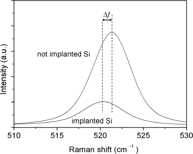
Raman spectra obtained on bulk silicon and on implanted Si sample
By using a bond polarizability model it has been found that this model can give a good description of the scattering intensity from optical modes.[12] The polarizability of the whole system is calculated as a sum of independent contributions from each bond; in this way, using the equation below (1) we made an estimative of size of our clusters, through the relation:

f(L) is the frequency of Raman phonon in a nanocrystal with size L, f0 is the frequency of the optical phonon at the zone centre, a is the lattice constant of silicon (a=543×10−12 m), A=47.0 cm−1 and γ=1.44 are parameters used to describe the vibrational confinement due to the finite size in a nanocrystal. Then considering equation (1) we obtain the value of (50 ± 10) nm for the clusters diameter size.
3.2 Surface analysis
The scanning tunnelling microscopy has been used to analyze the superficial features of implanted samples. Figure 2 shows typical results obtained onto implanted region. The morphology of the surface is shown in Figure 2(a) recorded in the “topographic” modality, the corresponding conduction map at Fermi level is shown in Figure 2(b). The topographic image showed that the surface is covered with a dense array of nanostructures, having mean size of about 50 nm, systematically oriented with respect to the substrate in the crystallographic direction (110).
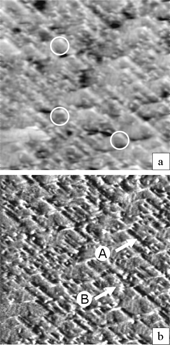
Typical 500 × 500 nm (a) topographic images of the Si implanted surface collected in the constant current mode; some of the 50nm size clusters were highlighted; (b) conduction map at Fermi level
The conduction map images shows contrast due to local conductance variation with high spatial resolution. At Fermi level the brighter regions represent areas with higher density of electronic states (LDOS) compared to that of the darker areas and would therefore be expected to be more conductive. The map clearly shows that the electronic structure of the surface was not homogeneous. Comparison of Figure 2(a) and (b) also indicates that the in homogeneity cannot be attributed to any topological feature of the surface and it must be assumed that the bright contrast regions are due to the nanosized structure grown during the ions implantation.
Further information on unevenness in the local conductive processes is better determined by scanning tunneling spectroscopy. By ramping the tip bias with respect to the sample, STS curves were obtained from dark and bright regions of Figure 2(b), marked A and B respectively.
We compare the different regions of the samples with respect to tunnelling current (I) as well as normalized differential tunnelling conductivity (dI/dV)/I/V. This is because although the ratio dI/dV is proportional to the DOS, it contains voltage dependent tunnelling matrix element. The logarithmic ratio dlog(I)/dlog(V)=(dI/dV)/I/V gives a more accurate representation of the surface DOS eliminating the tunnelling matrix element.[13] The I-V curves (figure 3), obtained from the regions at different electrical contrast, show that the tunnelling current is higher for bright region, in addition the I-V characteristic-curves are symmetric.

Typical I-V curves of dark regions (A) and bright regions (B) of Figure 2b
As a first approximation, the LDOS is fitted as a parabolic function of energy, e.g., dlog(I)/dlog(V)≈DOS∞ | (E-Ex) |1/2 where Ex is the distance between the Fermi energy EF and the edge of band with zero DOS. The cross-over point of the extrapolated DOS is determined by using the parabolic fit. Considering free electron formula,[14] the density of states of conduction and valence band is given by:

where m*e and m*h represent the effective mass of electron and holes, respectively.
In Figure 4 are reported the fit of LDOS using equations 2 with m*e = 0.9m0 and m*h= 0.15m0.[15] The best-fit curves have been obtained for an energy gap of 0.85 and 1.00 eV for bright and dark region respectively. These results suggest that the high-energy ion implantation has led, at the nanoscale level, high electronic inhomogeneity of the material surface.

Normalized dynamical conductance curves of dark regions (A) and bright regions (B) of Figure 2b.
3.3 Electrical characterization
The variations of d.c. electrical resistivity (ρ), Hall mobility (μ) of the oxygen-implanted silicon with temperature are shown in Figure 5 respectively for a representative sample. All the plots shown in Figure 5a-b indicated two distinct domains demarcated at temperature of about 250 K.

The variations of (a) d.c. electrical resistivity (ρ), (b) Hall mobility (μ) of a Si implanted sample with temperature.
Electron transport in the implanted samples at relatively low temperature could be explained by thermally activated hopping between localized states near the Fermi level.[16] In the variable range hopping (VRH) process the general form of the temperature dependence of conductivity (σ=1/ρ) is given by: [17]

where the pre-exponential factor σ0 may be either independent of T or a slowly varying function of T while T0 (= e2/ε0εra, a−1, ε 0 and ε r being the electron localization range, free space permittivity and the dielectric constant of the material respectively) is a constant of the material.
The value of the exponent p (0.25 < p < 1) depends critically on the nature of the hopping process. The values of the exponent p could be obtained from the slope of the plot (figure 6) of ln[W(T)] versus ln(T) where [18]
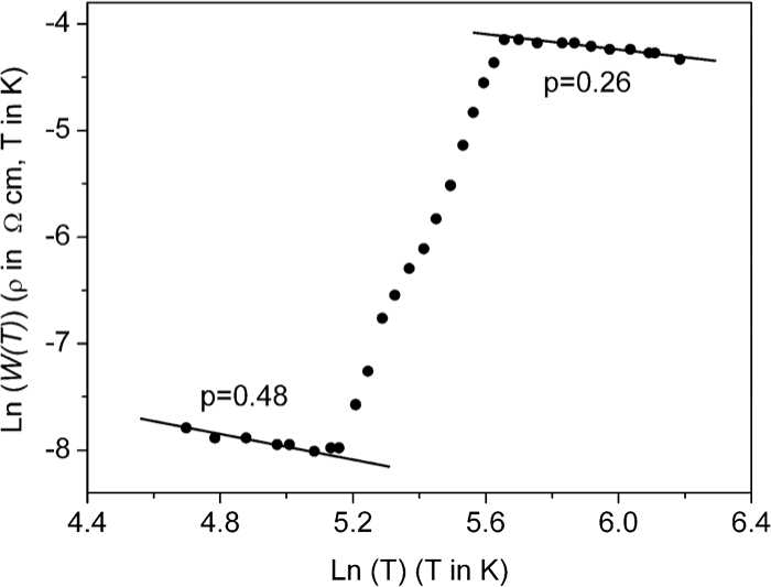
Plot of ln[W(T)] versus ln(T)
It may be observed that the experimental data for lower temperature of measurements follow the Efros and Shklovskii (E-S) model with p near the value of 0.5 (p=0.48). In the low-temperature regime the charge transport seems to be governed by a Coulomb-dominated hopping between strongly localized electronic states at the Fermi level.[19] On the contrary for higher temperature the experimental data suggest a conduction regime dominated by hopping mechanism according to the Mott's model with p near the value of 0.25 (p=0.26).
For a transport corresponding to “soft” Coulomb gap (p=0.5), the density of states, g(E) would have parabolic behaviour in the Coulomb gap. It is assumed that the density of states would level off when g(E) equals go (the Mott density of localized states at the Fermi level which remains unperturbed by the Coulomb interaction).
In our samples we have taken that the cross-over from E-S model to Mott's hopping was observed at the temperature of about 250 K.
The electronic density of states (LDOS) near the Fermi level is an important physical quantity for understanding electrical transport mechanisms in strongly localized systems, such as impurity bands in doped semiconductors and nanostructured materials. These consist of sites with random positions and random energies.[20] At low temperatures the electrical resistivity of such systems is governed by variable-range hopping (VRH), which means that the activation energy for a hopping process decreases continuously with temperature. In localized systems the Coulomb interaction creates a deep depletion of the one-particle DOS near the Fermi energy EF. Efros and Shklovskii (ES) called this depletion “Coulomb gap”.[21]
A crossover between these two temperature laws has been predicted theoretically [E-S]. Indeed, there is ample experimental evidence for such a crossover,[22] although the temperature range where the Mott law is visible depends on the material, especially on the nanostructures present.[23] According to the traditional interpretation of this crossover the energy range of the phonon-assisted tunnelling (hopping) becomes larger than the width of the Coulomb gap above the crossover temperature. In this case the Coulomb gap does not affect the hopping resistance, thus resulting in Mott's law.
Now, for the justification of the applicability of the E-S model to these nanocrystalline composite samples, the following criteria have to be satisfied so that VRH within the Coulomb gap becomes the most dominant transport mechanism
- Whop > kT or To > T
- Rhop > d
- Δ> Whop
Where Rhop = 0.25 αm−1(T0/T)1/2 is the hopping distance, Whop = 0.5k(T0T)1/2 is the optimum hopping energy, Δ is the Coulomb gap, α m is the tunnelling exponent.
From the above studies on the electrical conductivity of the implanted Si, we can see that both Mott and E-S variable range hopping were operative on the same sample in different ranges of temperature. The cross-over temperature between the two types of VRH is determined by the half width of the Coulomb gap.
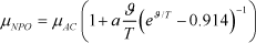
In order to study the scattering effect in Si implanted samples, we have examined the dependence of mobility with temperature (figure 5b). We have found that in the temperatures range investigated a single scattering phenomenon was not adequate to explain the experimental data. Considering additional contributions from polar (μPO) and nonpolar optical (μNPO) parts, the mobility (μ) can be expressed as:[24]
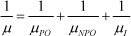
where μI is the mobility due to ionized impurity scattering:

The combined acoustic (μ AC ) and non-polar optical (μUPO) mobility may be expressed as:
The acoustical-mode-scattering mobility (μ AC ) is given by:

The polar mobility (μPO) may be expressed as
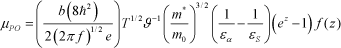
and εα is the limiting value of the high frequency dielectric constant, while εs is the static dielectric constant, z=ϑ/T and f(z) is a function which may be approximated in the range of 120-300 K by 0.48exp(0.18z). The values of the density (D), average velocity of sound (u), the deformation potentials for acoustic (EAC) and non-polar optical (ENPO) phonon and the characteristic temperature (ϑ) of the optical phonons used to evaluate the different contributions towards mobility are shown in Table 1. It can be observed (figure 5b) that the experimental data fitted well with the theoretical curve when the combined effects for different scattering mechanisms are considered.
Values of the different parameters used to evaluate the different contributions towards mobility

4. Conclusions
Structural and electrical characterization of high energy oxygen implanted Si samples were performed and revealed that the sample surface was covered with a dense array of about 50 nm tetragonal nanostructures systematically oriented with respect to the substrate. Resistivity and Hall effect measurements evidenced that the electron transport in the implanted Si samples could be explained by thermally activated hopping between localized states.
Despite the achievement of high mobility, the electronic transport of the nanostructured films is poorly understood. [30–33]. It is known that the mobility is highly sensitive to the crystallite grain size, and that the grain size and morphology depend on assembling and treatment procedure. Indeed, D. Knipp et al. [34,35] evidenced that the electronic transport of polycrystalline films are also strongly affected by the roughness of the substrate. Gleskova et al. show that tensile strain parallel to the film increased the electron mobility of n-type amorphous silicon whereas compressive strain decreased the electron mobility [36].
Certainly, MeV ion irradiations may lead to changes in surface morphology. It has been known for some time now that plastic flow of massive amounts of atoms, of the order of tens of thousands, may occur per ion impact.[25] Changes in surface topography have been attributed to localized thermal spike-induced melting, in addition to plastic flow due to surface tension forces. It is interesting to note here that we have obtained permanent features on the surface due to ion irradiations, modifying deeply physical properties of the samples, particularly their electrical behaviour.