
Abstract
In consumer electronics, Organic LED (OLED) has become mainstream display technology. Using organic materials, opto-electronics devices have become extensively desirable for various reasons. One of the fundamental properties i.e., flexibility permits to fabricate electronic circuits on flexible substrates to make these devices bendable and stretchable. This paper provides a review on various terms of OLED like fabrication methods, operation of OLED, its categorization, few OTFT driven OLEDs, stability issues of white OLED and various applications of OLED based on sensors, display, and lighting. Different lighting devices like incandescent bulb, tube light, CFL, LED and OLED are compared on the basis of their efficiency and lifetime. The comparison highlights that the LED provides good lifetime, however, for OLED it depends on the organic semiconducting materials responsible for emission. Different layers such as charge injection layers, transport layers and blocking layer to refine the properties of organic LEDs are also studied and compared. Addition to this, a low-cost methodology is also incorporated for the fabrication of flexible devices.
Introduction
The Organic LED is a carbon-based nascent technology in the field of displays, wherein thin films of specific light emitting organic materials are utilized. Owing to its high performance with respect to image quality, large fabrication area [1], flexibility [2, 3], low power [4] and design cost these devices have been successfully inducted for displays applications. Fabrication of OLED includes deposition of various organic semiconducting materials between the electrodes, each of these materials being used for a specific purpose. With the application of suitable voltage, a bright light is emitted by the device. Luminescence is one of the deciding factors to achieve uniform light output. The significant improvement in the performance of these devices is a direct result of developing novel methodologies such as charge transport layer, blocking layer, etc. Consequently, the performance parameters including luminescence and current density have illustrated significant amelioration. The present article is focused on reviewing various aspects related to these aspects.
Since the advent of modern-day lighting technology if various products are compared then incandescent lamp can be considered as one of the oldest. Table 1 encapsulates efficiency and lifetime of various technological improvements over several decade in this arena. This includes efficiency and lifetime of 15 lu/W and 1000 h respectively for incandescent lamp. The next significant improvement in this aspect was the tube light, renowned for it high efficiency of 108 lu/W and a lifetime of 25000 h. It took a substantial time before next important breakthrough was achieved, that was in the form of CFL. This device demonstrated corresponding efficiency and lifetime of 50 lu/W and 12000 h. Due to its cost effectiveness and reliability, it easily replaced incandescent bulbs and at times even tube lights.
Comparison of efficiency and lifetime of lighting products
Comparison of efficiency and lifetime of lighting products
All these advancements have paved way for solid state lighting devices, especially the conventional LEDs. These devices are based on semiconductors depicting a high efficiency in the range of 100–150 lu/W, that is recorded the highest as compared to earlier products. It also possesses a high lifetime of 50000 h [5], owing to their reliable fabrication. Presently, every researcher is focused on energy conservation wherein these solid-state devices are gaining prominence. OLED is one device that can perform better than conventional solid state devices pertaining to energy consumption. These devices also depict a good efficiency of 100 lu/W, however, its lifetime varies depending on the color of light emission. Recorded lifetime for red, green and yellow color as 80000 h, 40000 h, and 7000 h [6, 7] correspondingly as highlighted in Table 1. These devices are fully capable of competing with conventional solid state devices barring their lifetime where substantial improvement is required.
The working of OLED is very similar to the conventional LED but structure wise both are very different. In organic LEDs, no doing is incorporated. For the conduction, conducting polymers are utilized in places of p type and n type semiconductors for the generation of holes and electrons, respectively. There is total four layers used in the basic structure of organic LED as depicted in Fig. 1. The bottom is used as substrate. Addition to this, there is a top layer i.e., cathode which is acting as electron generators and above substrate there will be a layer i.e., anode which is responsible for holes generations. In between cathode and anode there is a most important layer of OLED where light is produced. This layer is called emissive layer.
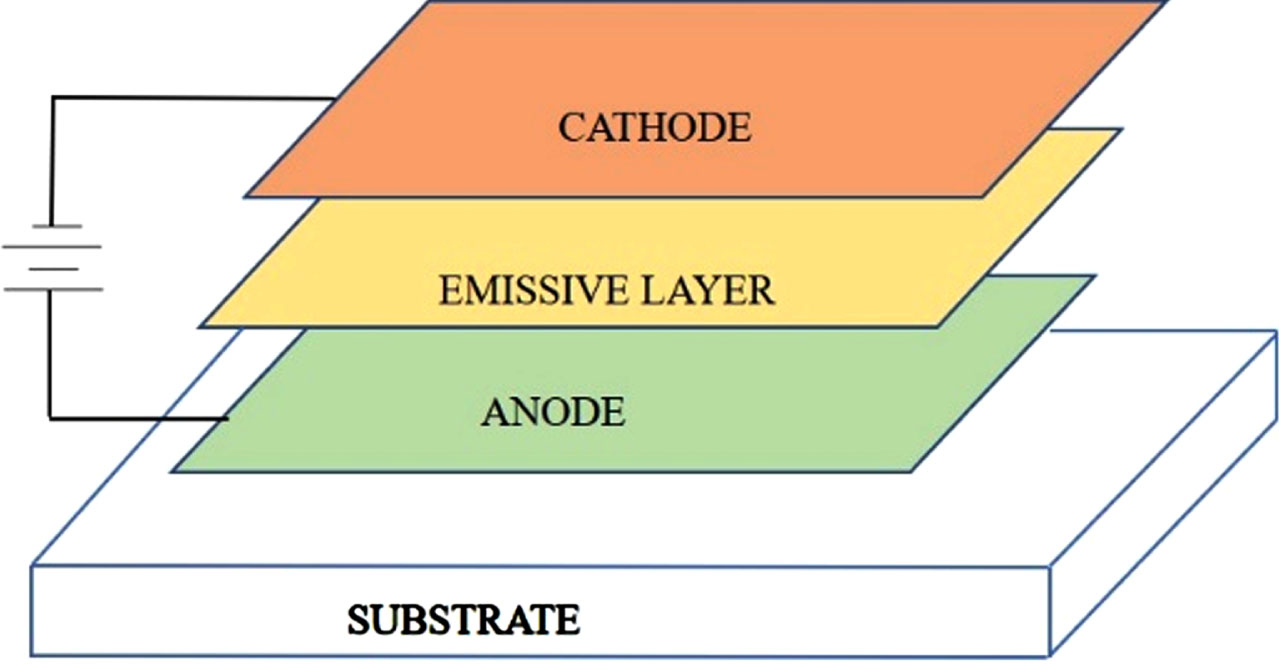
Basic structure of OLED.
When a battery is connected to both electrodes (cathode and anode) in forward biasing mode, cathode and anode starts collecting electrons and holes from negative and positive battery terminal, correspondingly. The electrons and holes now travel towards the emissive layer where recombination of these charge carriers takes place and light is generated.
The organic LEDs is a diversified field that included multiple facets. Therefore, these are classified into varying categories depending on their usage, and technologies incorporated for fabrication. The current section briefly introduces basic categorization of OLED based on their circuit techniques, architectural modifications and color of emission.
Circuit based categorization
Here, the OLED devices will be characterized on the basis of circuit.
PMOLED
The acronym stands for Passive Matrix Organic Light Emitting Diode. Its architecture comprises of strips of cathode and anode, wherein each intersection is a pixel resulting in the light output [8]. The light emission from these intersections is controlled by the amount of current flowing within them. The fabrication process for PMOLED is simple yet at the same time their power consumption is deemed to be highest compared to any other OLED circuit. Resultantly, these devices are limited with respect to their size and resolutions making them suitable for small displays utilized in mobile phones and MP3 players.
Various researchers have been working on PMOLED circuits in recent time. Yan et al. [8] reported a 3.5-inch passive matrix OLED which does not contain any dead space on device sides. This results in smooth stitching of many PMOLEDs to design larger panel. Afterwards, Su et al. [9] designed a 7-inch full color PMOLED where roll-to-sheet process for lamination is incorporated to laminate 100μm PEN substrate. This process helps in achieving bubble free lamination. Addition to this, Uttwani et al. [10] studied a organic LED matrix and created defects purposely to investigate the possible visual manifestations.
AMOLED
the Active-matrix OLEDs [11] varies from PMOLED as these consists of continuous sheet of cathode, organic semiconductor material over which layers of anode are deposited. The anode layer is controlled through a matrix of thin film transistors (TFT), that results in low power requirements. Additionally, the charging rate is fast and hence these can be utilized for large size displays including TVs, monitors, electronic billboards etc.
Many significant efforts have been put in by the researchers to enhance the performance of these devices. Some of these include, Boera et al. [12]. Their work included SIBO i.e. single inductor based bipolar outputs, resulting in DC-DC converters used for AMOLEDs. These are capable of generating desired twin voltage of different polarity with the single inductor device. These circuits have an input voltage range of 2.4 V - 4.9 V and can generate output values of +5 V and –6 V with a max. o/p current value of 0.6A at the load.
Another research group, Steudel et al. [13] were able to fabricate flexible AMOLED that incorporates the OTFT backplane. Overall the device depicts a resolution of 85 DPI along with a 75% aperture ration and luminescence output of 200 cd/m2. Mo et al. [14] worked on developing an amorphous oxide based thin film transistor for large panel AMOLEDs. The device so developed illustrated high performance including mobility: 21 cm2V-1s-1, ION/IOFF greater than 108 and subthreshold slope of 0.29 V/dec.
Categorization based on architectural changes
In this sub-section, characterization of organic LEDs will be discussed in terms of their architecture.
Top emitting OLED
These OLEDs are capable of emitting from the top and hence are generally fabrication on a reflective or a solid substrate. Their unique emission makes them suitable for AMOLED display circuits. Figure 2 is depicting top emitting OLED. Additionally, these devices find their optimal usage for credit and debit cards wherein a smart card is required.
Top emitting OLED.
Some researcher working with TEOLEDs include Qu et al. [15]. Their group worked on high efficiency green phosphorescent OLEDs depicting improvement of EQE from 20- to 30%. Liu et al. [16], worked on MI: “mixed interlayer” of Poly [(9, 9-dioctylfluorenyl-2, 7-diyl)-co-(4, 4′-(N-(4-secbutylphenyl) diphenylamine)) (TFB) and Poly (9-vinylcarbazole) (PVK). The layer was deposited between PEDOT:PSS and emissive layer for improved luminescence as a result of refined hole injection. Similarly, Lin et al. [17] developed a new cathode blocking layer Yb (ytterbium). This material inhibits the migration of Silver (Ag) atom within the cathode resulting in ameliorated thermal stability of TEOLED.
As the name signifies, these are the OLEDs through which light can travel in both the directions. These are typically see through OLEDs [18]. This device supports both the circuit configurations discussed in the previous section and also provide a good contrast even in the sunlight. Hence, these often find their usage in “Heads-up-Displays” i.e. HUDs. Some research work carried out for this particular device are discussed next.
Qin et al. 2016, [19] proposed the simulation method for blurred images for see through transparent OLED. Modulation transfer function and the pattern’s characteristics were obtained for calculated images and the once captured through camera. The error between them were obtained as 5.7% and 5.6% respectively. Thereafter, in 2020, Song et al. [20] reported a highly reliable transparent cathode for these devices. They were able to achieve a current efficiency value of 36 and 18 cdA-1 for bottom and top side emission in transparent OLEDs. Most recently (2022) Tsai et al. [21] developed a T-OLED utilizing a high transmittance cathode resulting in enhanced flexibility. Herein, mechanical debonding technique is used for achieving a debonding force to stabilize the OLED device.
Foldable OLED
One of the prominent advantages of organic LEDs is their flexibility. Hence these foldable devices are developed using a flexible substrate. These devices require strong but flexible materials to reduce breakage. Their possible utilization is in modern day cell phones, GPS devices and foldable big screen displays. These foldable devices are capable of generating fast response, crisper picture resolution owing to high contrast. Flexibility being one of the primary usage, a lot of researchers focused on this particular aspect some of which are discussed in the succeeding paragraph. The structure of foldable OLED is illustrated in Fig. 3.
Foldable OLED.
Takahashi et al. [22] proposed a high resolution 13.3” “8K4K” 664 PPI foldable organic display in conjugation with crystalline oxide based semiconductor FETs. The entire design consists of single capacitor and three transistors for each pixel circuit. After this, Han et al. [23] depicted a stress free foldable “SFF” hinge with the inclusion of virtual axis structure “VAS” and modulized assembly structure: “MAS”. The overall architecture enhanced the folding reliability to 200K with less than 20% torque reduction.
The white OLED contains all red blue and green colors as highlighted in Fig. 4. White OLED [25] utilizes less energy to generate a brighter light comparatively. Hence, they become more environment friendly on comparing with other color OLED. Except white OLED; red, green and bule OLED also exist. The type of materials is mainly responsible for color emission in OLEDs. Generally, green and red OLED materials have better luminescence when compared to the blue OLED [26]. The curve (Fig. 5) below is comparing the data of six white organic LEDs W1, W2, W3, W4, W5 and W6 [27–32] in terms of luminescence. The maximum value is obtained as 170,000 cdm-2.
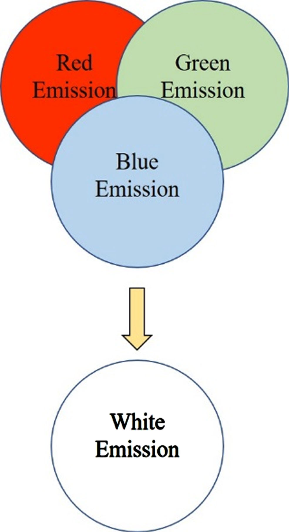
White OLED from RGB OLEDs.
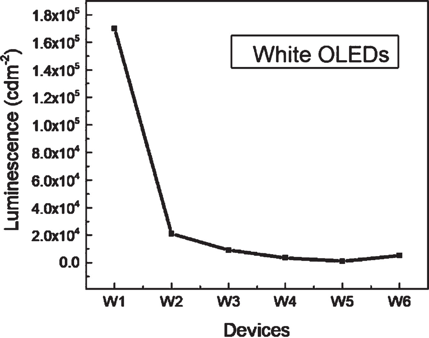
Comparison of WOLEDs in terms of luminescence.
The researchers have explored WOLEDs widely with respect to their efficiency and operational stability. In 2015, Du et al. [33] prepared a hybrid white organic LED. In the research, the luminous efficiency is reported as 12.4% at 1000 cdm-2. As well as, additional performance parameters like power efficiency and current efficiency are obtained as 17.6 lmW-1 and 27.5 cdA-1, respectively. Afterwards, Yang et al. [34] discussed about sandwiched CCL (color conversion layer) for blue organic LED to make WOLED. The proposed device showed high color stability. Moreover, Sun et al. [35] fabricated a warm white OLED which consists of four emissive layers and the pure WOLED containing three emissive layers. The device reported current efficiency, power efficiency and EQE for warm WOLED as 69 cdA-1, 60.19 lmW-1 and 20.93 %. On the other hand, for pure white OLED the same parameters are achieved as 60.48 cdA-1, 51.32 lmW-1 and 16.90 %, correspondingly.
In OLED, during the manufacturing process, applying layers to substrates is a most complicated and important process. Table 2 below is illustrating the materials and processes of different layers such as anode, OSC (organic semiconductors) and cathode.
Various layers and their materials along with processes
Various layers and their materials along with processes
There are several methods for device fabrication available nowadays. Some of these methods are mentioned below.
This method is considered as low-cost method among all deposition methods [36, 37]. In this technique, a carrier gas is chosen for the movement of evaporated organic molecules on cooled substrate as utilizing the carrier gas provides high efficiency and reduces fabrication cost. Kajiyama et al. [38] presented an organic LED utilizing a in-situ contact shadow mask patterning technique using laser ablation. In this work, the resolution and aperture ration are obtained as 338 ppi and 60%, correspondingly. Moreover, Sanderson et al. [39] studied the performance variations of solution processed and vacuum deposited devices by doing molecular dynamics simulations.
Vacuum Thermal Evaporation (VTE)
In this technique, organic molecules are heated up and thereafter condensed onto cooled substrates [37]. Due to good accuracy and heating methods, VTE is quite expensive methods for the deposition of thin layers. Hence, other techniques are preferred over this technique for large area devices. Various OLED devices have been investigated using this technique by many researchers. Liao et al. [40] prepared an OLED using VTE method. The proposed device exhibited significant performance and provided EQE as 27.6% at high luminescence.
Thereafter, Song et al. [20] presented a transparent cathode with the help of thermal evaporation technique. The proposed device provided better electron injection and current efficiency from top and bottom sides emission are achieved as 18 and 36 cdA-1, correspondingly. Moreover, Kim et al. [41] reported a metal patterning to achieve self-metal patterning with thermal evaporation technique. In this report, he received excellent patterning properties from the material polyfluoro-tetracosane which have lowest surface energy.
Inkjet printing
Inkjet printing is the mostly used process in comparison with other. In this technique, organic thin layers are deposited using spraying method as depicted in Fig. 6. It is very similar to paper printing process [42, 43]. In this section, a low-cost fabrication technique is discussed. This technique is utilized by Cho et al. [44]. Figure 7 is highlighting the technique procedure in detail.
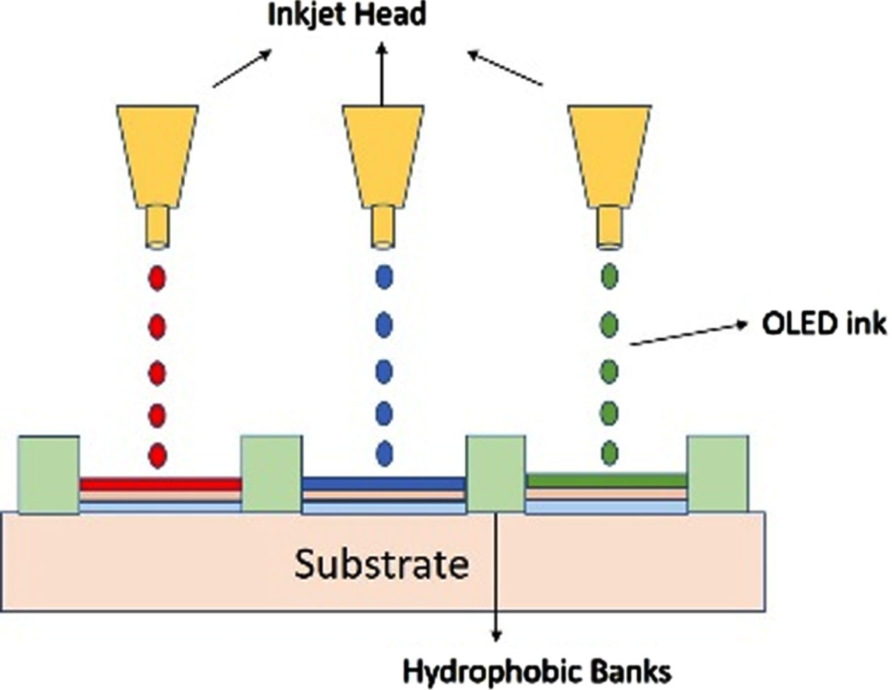
Process of inkjet printing.
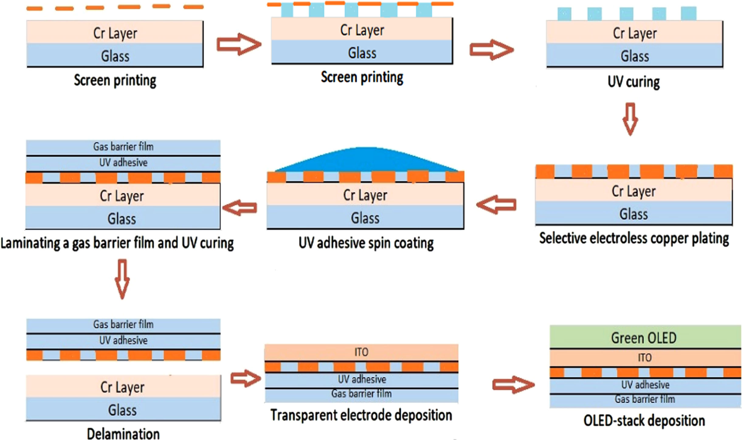
Fabrication steps of flexible integrated substrate OLED.
In this work, V-I characteristics of the proposed devices are drawn. Additionally, luminescence factor and electroluminescence spectra are investigated. This research provided an effective low-cost method for flexible organic LEDs.
The property of emission of light by a material without providing any external heat is called luminescence. Various semiconductors gain energy in different forms and participate in the generation of light. Generally, there are two steps which are incorporated for light emission which are, 1) excitation of the system and 2) subsequent emission of the photons. In the organic LED, type of organic materials and supply voltage and color emission are very important terms to refine the luminescence.
The luminescence remains the most important performance parameter in comparing with other parameters like current density, power efficiency, current efficiency, external quantum efficiency (EQE) etc. as organic LED is a self-light emitting device [45]. Figure 8. outlines the growth of luminescence over 15 years. The peak luminescence is obtained as 92,455 cd/m2 [46] during 2015–2021. The minimum value is reported as 100 cd/m2 in 2015 [47]. This parameter has been explored by various researchers. Park et al. [48] studied the auxiliary metal electrode effect on a large white organic LED of 15×15 cm2 dimensions having uniform luminescence. In this research, an organic LED panel showed luminance uniformity of 90% at 200 mA and 85% at 500. Han et al. [49] studied the improvement in the luminance with the help of micro lens array (MLA), it majorly depended of luminescence area, viewing angle but hardly depends on the driving conditions. Researchers Aasha et al. [50] explored LUMO and HOMO of Alq3 material and compared with Phosphorene. It is noticed that Phosphorene has lowest band gap and this was the main reason for luminance improvement.
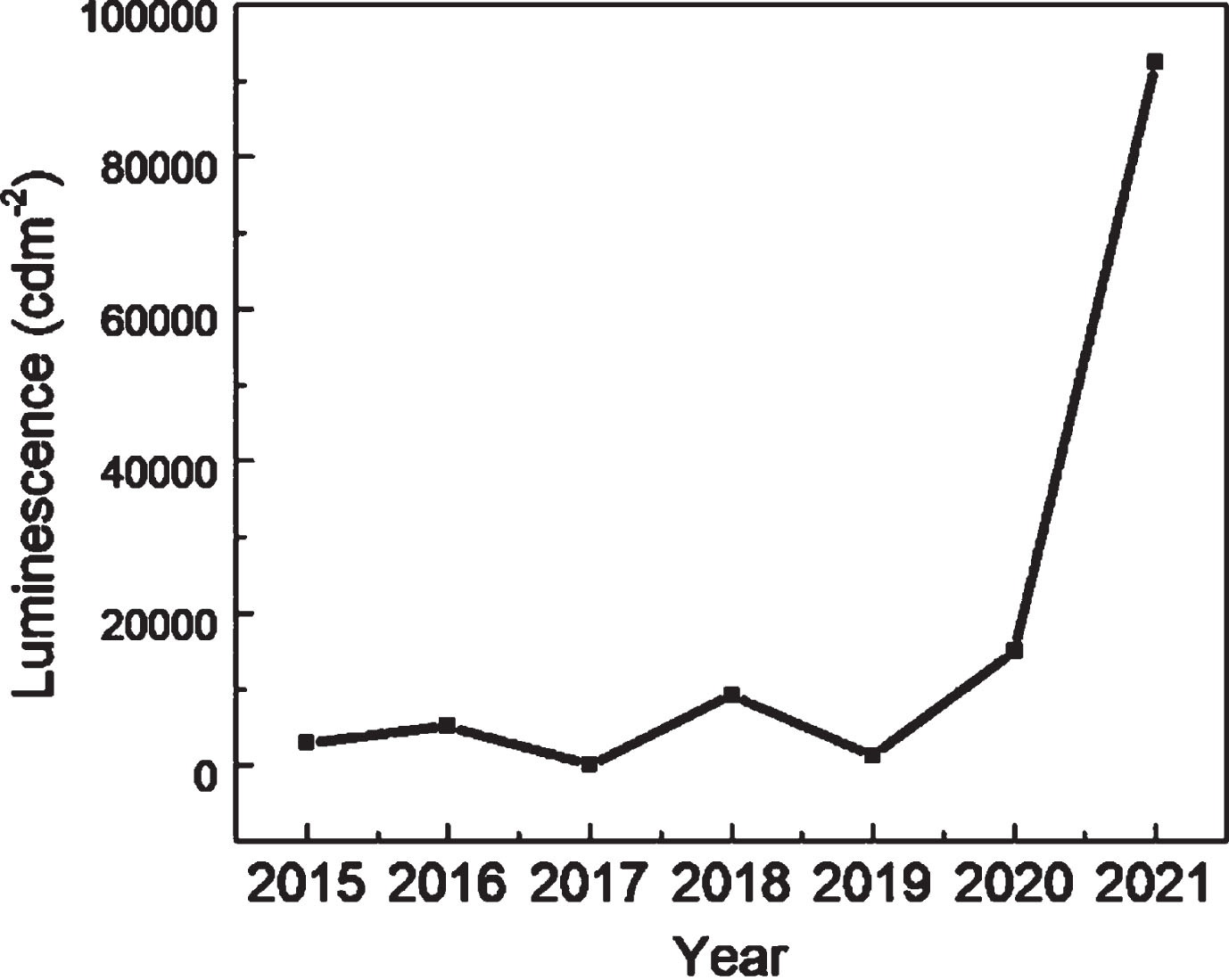
Luminescence progress over 6 years.
In OLED devices, mobility of electrons and hole (charge carriers) is an important parameter. The electrons are expected to form exciton with the holes from anode side when electrons are injected in organic layer from cathode. Each electron which travels from cathode to anode should form exciton to have highest efficiency. In order to generate this and to get maximum exciton generation the charge ratio must be in adequate amount.
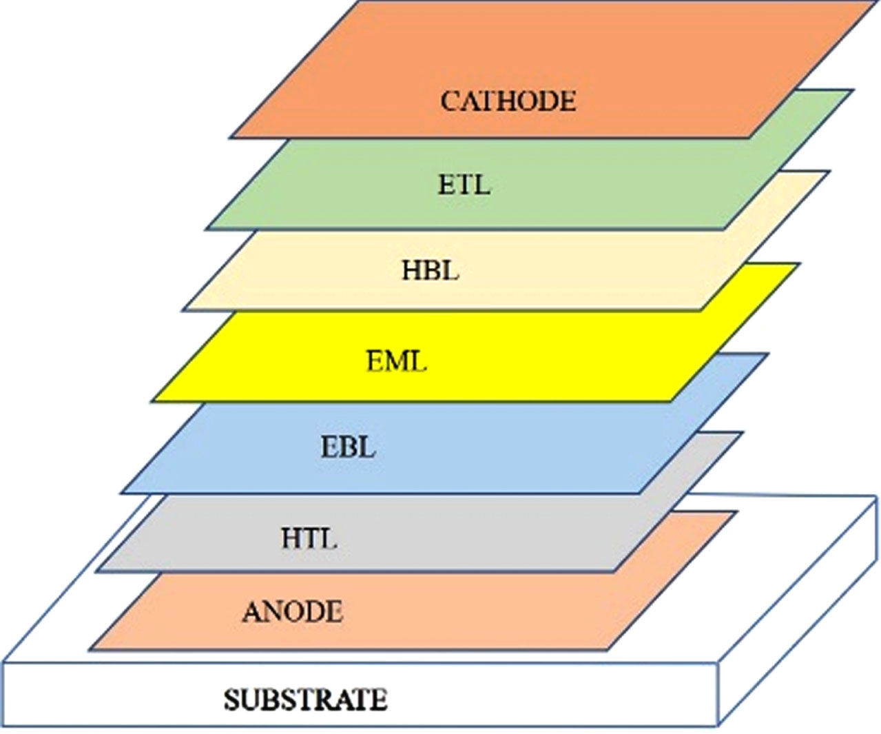
In case of organic materials, the mobility of hole is always greater than electrons. Due to the mobility difference of charge carriers the recombination happens close to the cathode layer and as a result we get quenching of excitons. We can overcome this problem with matching the mobility of electrons and holes. This is shown in Fig. 9, where we have added few more layers such as hole and electron transport layer (HTL and ETL), hole and electron injection layers (HIL/EIL) and hole and electron block layer (HBL and EBL) in our OLED structure [51, 52]. We have included short discussion in Table 3 all the layers which are required for a multi-layered structure.
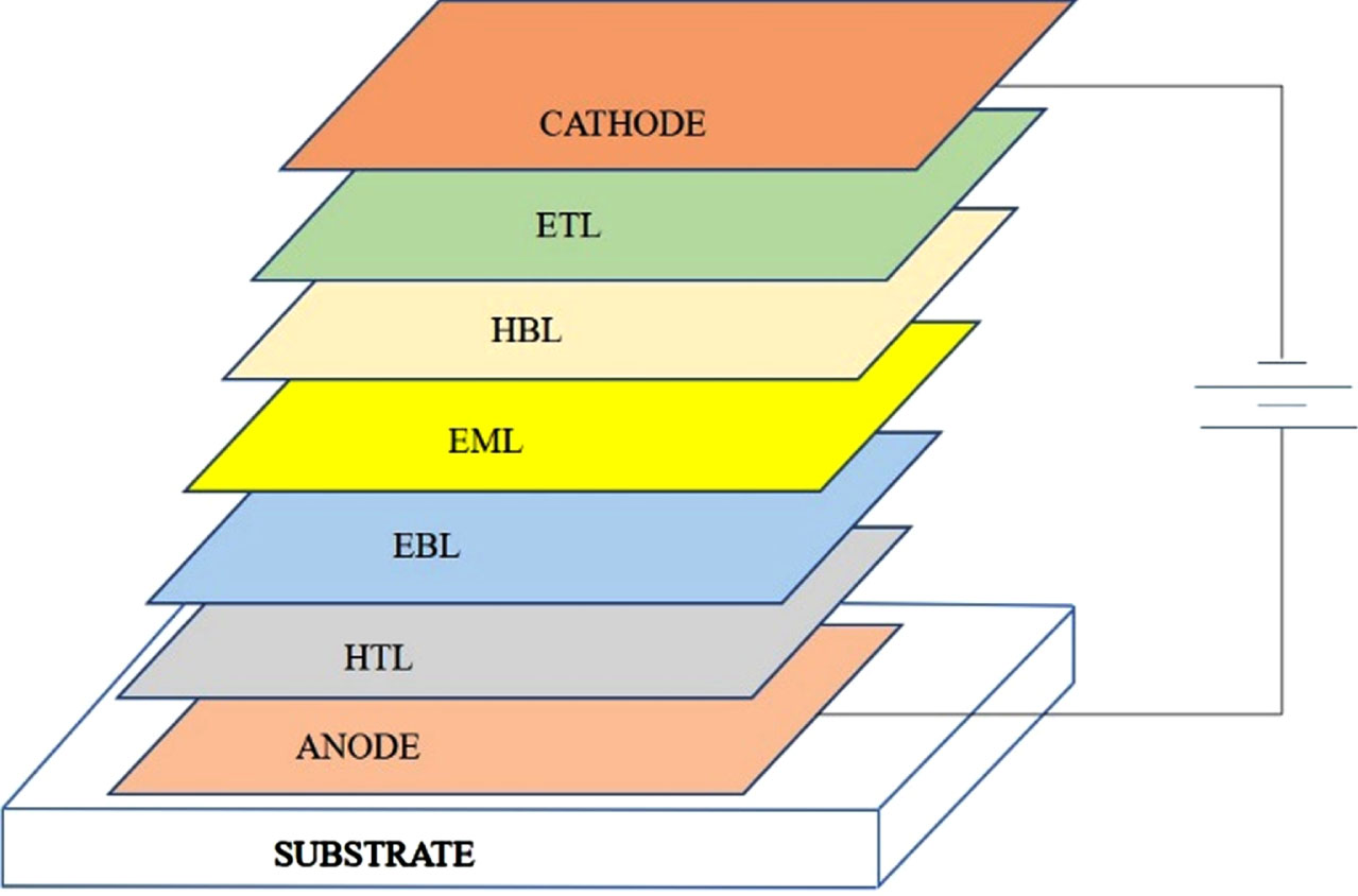
Multi-layered structure of OLED.
Purpose of multilayer of OLED
A lot of researchers have done research in these layers and proposed multiple ways to improve performance of these layers [55–57]. Zhang et al. [58] has done research in finding the role of Fe3O4 for enhancing the hole transport and injection by ultraviolet photoelectron spectroscopy. They found that Fe3O4 has varied effectiveness when it gets injected in various host materials. By lowering the hole injection barrier OLED properties is improved. Whereas, the enhanced hole transport improved the properties of OLEDs with 3-methylphenylphenylamino because of good charge transfer formation.
As compared to other layers, emissive layer is the most studied layer as within this layer light is garneted. Various materials have been explored to refine this layer. Yoo et al. [59] prepared a blue OLED with an emissive layer having double dopants FIr6 and FIrpic. The paper reported peak luminous efficiency of 24.8 cdA-1. Thereafter, a highly efficient hazard free blue OLED is investigated. The device exhibited characteristic parameters such as EQE and current efficiency as 24.5% and 24.4 cdA-1, correspondingly. Afterwards, using a double emissive layer a highly efficient OLED is presented by Sharma et al. [60] which calculated EQE as 39 %. On the other hand, Fujimoto et al. [61] discussee an OLED having a HBL of the material 2,4,6-tris(biphenyl-3-yl)-1,3,5-triazine (T2T). In this research, the lifetime is refined by 9 times.
Organic TFTs act as a backbone for organic LEDs. These transistors have been enormously investigated because of their various application such as displays, wearable AMOLEDs, smart sensors, RFID etc. [62–66]. This section will incorporate some various structures of OTFTs. Figure 10 is illustrating the various structures of OTFT such as planer, dual gate, vertical and cylindrical OTFTs. Generally, bottom gate structures are preferred over top gate. The reason is that in bottom gate active layer deposition is quite easier due to its structural changes. Additionally, top contacts are preferable over bottom contacts as less morphological disorders take place in top contacts.
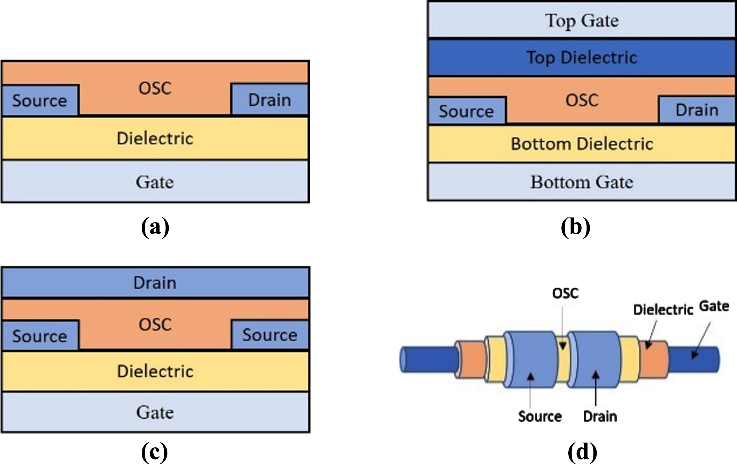
Different organic thin film transistors: (a) Planer, (b) Dual Gate, (c) Vertical, and (d) Cylindrical OTFTs.
Lot of research work has been done to investigated these mentioned OTFTs. Zuo et al. [67] presented gate dielectric layer with polyimide polymer. The bottom gate bottom contact with the reported dielectric exhibited significant performance based on carrier mobility and I ON /I OFF as 1.23 cm2V-1s-1 and about 5×10⁵, respectively. In recent time, Steckmann et al. [68] proposed two devices with high electron mobility using ultrathin P(NDI2OD-T2) films for top and bottom gate. Furthermore, Singh et al. [69] discussed a dual gate TFT having PEN substrate using solution-processed technique. The charge carrier mobility is obtained as 0.37 cm2 V-1s-1.
On the other hand, Chen et al. [70] proposed a vertical quantum-dot light emitting transistor using VOTFT. The device exhibited maximum current efficiency as 37 cd/A. Moreover, recently, Knepp et al. [71] presented VOTFT with pentacene using solution-processed technique. Figure 11 (d) is illustrating cylindrical OTFT. In this type, all the layers are adjusted in cylindrical manner. These devices attain salient properties such as good bending stability and hysteresis free operation [72].
Several applications based on organic LED display have been proposed by incorporating organic TFTs as highlighted in Table 4. In 2012, image quality of an organic TFT driven OLED was refined by Nakajima et al. [73]. This was done by enhancing the performance of OLED and OTFT. Furthermore in 2017, Mizukami et al. [74] reported a 3.2 inches OLED driven by organic TFT using inkjet printing technique. The peak luminescence of the device is achieved as 125 cd/m2. The organic TFT showed very good mobility of 1.2 cm2V-1s-1. This made the transistor suitable for flexible color OLED.
Comparison of various OTFT-driven OLEDs
Comparison of various OTFT-driven OLEDs
Furthermore, Pal et al. [65] proposed an AMOLED driven by OTFT and studied the effect of various gate dielectrics onto it. It is noticed that stack dielectric-based pixel circuit achieves the peak OLED current of 0.6μA. Table 4 is representing the comparison of six different active-matrix OLEDs (D1 - D4) driven by organic TFTs. Here, the maximum luminescence is obtained as 64,459 cdm-2.
It is predicted that in near future technology competition will be more intense. This section is highlighting the applications of OLEDs based on display, light and sensors.
OLED Display
Initially, OLED devices was applied to display applications only. These devices contain many versatile benefits over inorganic devices such as high contrast, flexibility, fast response, color fidelity, wider viewing angle etc. [78]. In recent times, organic LEDs are being utilized in many display applications like smart TVs, personal data processor, mobile phones, smart watches, laptops etc. The big industries like LG and Samsung have launched commercially OLED display technology era by presenting 55-inch OLED TV in 2013. At present, there many industries which are contributing in the field of OLED display are: South Korea’s Samsung Electronics, Apple, BOE, Victoria Connaught, South Korea’s LGD, etc.
OLED Light
Light emission is the main feature of organic LEDs. Various research has been incorporated to study the light-based applications of OLED [79]. OLED lighting industry have reached to 1.7 billion dollars world-wide in 2020 [80]. Many countries like Japan, China, The United States, Europe have targets to increase funding in the OLED lighting market [81]. As well as, these devices are now exploring other fields such medical, industrial and advertising.
Sensor
Organic LEDs have been utilized in many sensor applications. An ultrathin active-matrix OLED is proposed by Kim et al. [82] which attain the property of capacitive touch sensor. Addition to this, Watanabe et al. [83] prepared an in-cell touch sensor using a foldable OLED device. The device properties remained unchanged even after 105 folding operations having 5 mm radium. Moreover, Tang et al. [84] discussed a self-capacitive touch sensor. This sensor enhanced the touch properties along with large touch panel in low ground mode with multi fingers.
Conclusion
Organic LEDs do not need any backlight hence these devices are considered as low power devices. These devices can be smoothly placed in large thin sheets as they are very flexible in nature. As the name suggests, OLEDs have self-luminous properties. Hence, the devices contain wider viewing angle. Having lot of salient features, there is still need of improvement in few characteristics’ parameters. One of these parameters is lifetime. Organic devices have less lifetime as compared to inorganic one. The lifetime of red and green is about 80,000 and 40,000 hours. On the other hand, yellow have quite shorter lifetime of approximately 7,000 hours only. This paper compares many aspects of OLEDs such as working, categorization based on various factors, its luminescence, stability and various applications. The paper also incorporates organic thin film transistor and reviews some OTFT driven OLEDs. OLEDs are also very sensitive to water. They can easily get damage by water vapors. In this paper luminescence and multi-layered structures are also reviewed. The research work of different researchers is compared and analyzed.