
Abstract
The research tends to suggest a spin-orbit torque magnetic random access memory (SOT-MRAM)-based Binary CNN In-Memory Accelerator (BIMA) to minimize power utilization and suggests an In-Memory Computing (IMC) for AdderNet-based BIMA to further enhance performance by fully utilizing the benefits of IMC as well as a low current consumption configuration employing SOT-MRAM. And recommended an IMC-friendly computation pipeline for AdderNet convolution at the algorithm level. Additionally, the suggested sense amplifier is not only capable of the addition operation but also typical Boolean operations including subtraction etc. The architecture suggested in this research consumes less power than its spin-orbit torque (STT) MRAM and resistive random access memory (ReRAM)-based counterparts in the Modified National Institute of Standards and Technology (MNIST) data set, according to simulation results. Based to evaluation outcomes, the pre-sented strategy outperforms the in-memory accelerator in terms of speedup and energy efficiency by 17.13× and 18.20×, respectively.
Introduction
Robotics, computational linguistics, computer vi-sion, and many other fields have adopted convolu-tional neural networks (CNN) to a large extent. CNN has a large number of parameters, which results in higher storage costs and longer latency. The GraphS architecture converts the existing SOT-MRAM into massively parallel computational units that can accelerate graph processing applications and provide extremely high internal bandwidth [1]. Deoxyribonucleic acid (DNA) short read alignment is proposed to be performed by the parallel processing in memory (PIM) accelerator, which is optimized through a novel data partitioning as well as mapping approach [2].
The novel ReRAM-dependent graph analytics accelerator could indeed enhance the workload density of crossbars interactively by employing a tightly-coupled bank parallel layout and handling significant graphs that frequently have skewed degree distributions [3]. Resistive memory (ReRAM) is used in the research to substantially improve performance in terms of energy efficiency. Efficient ReRAM-based accelerators are designed using the general concepts of processing-in-memory to enable both training and testing operations [4]. Nevertheless, writing operations typically perform longer and consume more power in ReRAM than they operate on DRAM. A SOT-MRAM-reliant PIM accelerator that fully facilitates floating point precision might have emerged as an excellent solution to lessen the dominant data movement cost because it eliminates the need to access deep neural network (DNN) weights [5].
It is suggested that a Depth wise CNN In-Memory Accelerator (DIMA) depend on SOT-MRAM, and the multiplication as well as accumulation, two computationally expensive convolution procedures, are transformed into hardware-friendly addition operations in Add-Net [6]. SOT-MRAM, which combines the compute-in-memory (CIM) as well as near-memory systolic array to execute the system level assessment for DNN inference engines and obtain 93% and 51% higher energy efficiency, respectively. Considering the prevailing pattern, memory/computational capabilities and their interaction have invariably run into limits as DNNs have become more complex.
Higher writing latency and the need for data with a low bit-width were disadvantages of SOT-MRAM-based PIM. To resolve such concerns, a framework that uses design compression strategies, such as weight pruning and quantization, and incorporates the interchanging direction strategy of multipliers to further ensure the feasibility of the solution was pro-posed [7]. In order to trade off around power, load computation, speed, and accuracy, a dynamic channel-adaptive deep NN can change the involved convolution channel at run-time and further use knowledge distillation methodology to optimize and quantize the model, respectively [8, 9]. In order to effectively accelerate the training phase of GAN in non-volatile memory, a processing-in-memory (PIM) accelerator for Ternarized Generative Adversarial Network (TGAN) is suggested. This accelerator would be termed PIM-TGAN, and it is premised on SOT-MRAM computational sub-arrays [10]. However, there are a number of unavoidable downsides to the existing DRAM-based PIM designs, including excessive refresh/leakage power, multi-cycle logic functions, operand data overwriting, as well as operand localization. The contribution is as follows: The research proposes a SOT-MRAM-based Binary CNN In-Memory Accelerator (BIMA) to minimize the power consumption and an In-Memory Computing (IMC) for AdderNet to further boost the performance. And recommended an IMC-friendly computation pipeline for AdderNet convolution at the algorithm level, as well as observing that subtraction had extended latency compared to addition on iMAD. Additionally, the suggested SA is not only capable of the addition operation but also typical Boolean operations including subtraction. The SA performs READ, NOT, AND, NAND, OR, XOR, and Addition (ADD) functions natively and Subtraction (SUB) extensively. Evaluation outcomes show that the suggested methodology achieves 17.13× speedup and 18.20× energy efficiency. The organisation of the research seems to be as follows: Section 1 provides an introduction to the proposed work, while Section 2 provides related works. Section 3 comprises the proposed research. Section 4 explains the outcomes and the discussion. Furthermore, Section 5 concludes the research.
The organisation of the research seems to be as follows: Section 1 provides an introduction to the proposed work, while Section 2 provides related works. Section 3 comprises the proposed research. Section 4 explains the outcomes and the discussion. Furthermore, Section 5 concludes the research.
Related works
Chang et al. (2019) developed a non-volatile memory (NVM) dependent CIM using a Preset-XNOR operation with the SOT-MRAM. With relatively minor changes to the peripheral circuitry, PXNOR-binary neural networks (BNNs) carry out the XNOR operation of BNNs in order to speed up the computation of BNNs. Roohi et al. (2019) suggested an in-memory bit-wise CNN accelerator employing SOT-MRAM computational sub-arrays. It employs a state-of-the-art AND accumulation technique that performs a variety of low-bit-width CNN inference operations. Simulations show that, compared to ReRAM-based acceleration, modern CMOS-only approaches can be sped up with a 9.% increase in speed and a 5.4% improvement in energy efficiency, while maintaining the same level of inference accuracy as baseline designs. Kim et al. (2019) suggest NAND-Net, an effective design in order to reduce the computational complexity of in-memory processing for BNNs. Relying on the finding that BNNs possessed a lot of redundancy, each convolution was broken down into smaller convolutions, and any unwanted functions were removed.
Doevenspeck et al. (2020) describe an optimized SOT-MRAM for weight memory in Analog in Memory Computing (AiMC) systems that make it possible to modify the MTJ resistance to higher levels without modifying the writing by manipulating the tunnel barrier thickness. Angizi et al. (2018) present an accelerator system framework based on a in-memory convolution engine that can be utilized to speed up CNN inference and dramatically lower the energy consumption of convolutional layers, as well as requiring 3× less energy than the current RRAM-predicted equivalent.
Zhao et al. (2022) introduce a NAND-like spintronics memory (NAND-SPIN)-based PIM architecture for efficient convolutional neural network (CNN) acceleration. An easy data mapping method is utilized to boost parallelism and reduce data movements. Using the benefits of NAND-SPIN and in-memory processing architectures, experiments show that the proposed method can be 2.6 times faster and use 1.4 times less energy than current PIM solutions.
Bavikadi et al. (2020) analyse Non-Von Neumann computing architectures like IMC and PIM, and the additional difficulties and restrictions in IMC research, are explored to perform binary convolution without adding additional distinct logic circuits for computation. The important issue of PIM is that it uses excessive memory bandwidth and embedded logic units for handle data in memory, thus might result in remarkably minimal transmission energy as well as latency.
Amiee et al. (2019) established a Spintronic Logic-in-Memory (SLIM) XNOR neural network to accomplish energy minimization, enhance throughput, and improve accuracy compared to the traditional binarized CNN hardware. Chen et al. (2020) establish adder networks (Ad-derNets) to exchange these enormous multiplications within deep neural networks, specifically CNNs, for substantially lesser expensive additions to decrease computing expenses.
Huang et al. (2021) investigate a hybrid spin/CMOS cell (HSC) architecture in which the non-volatile data from the spin element as well as the volatile knowledge from the CMOS element could easily accomplish the XNOR operation in an in-memory computing approach. Kim et al. (2022) recommend adopting SLIM cells, which employ voltage-controlled magnetic anisotropy (VCMA) to maximize the memory cycle efficiency and enable efficient logic inside memories. Additionally, it is indicated that the crossing input source PIM (CRISP) design would substantially increase parallel processing and eliminate the additional memories, hence maximizing the advantages of SLIM cells.
Asad et al. (2022) investigated these challenges in their analysis of recent advancements in the design methodologies and efficient memory structure of the DNN accelerator. Additionally, the application of adaptive DNN computations in flexible memory systems will be examined. The analysis of new memory technology will be the last step. Ielmini et al. (2022) explore the state of IMC and its challenges from a device perspective and describe a reference implementation employing RRAM. Contemporary developing memories are contrasted in terms of their variation and conductance. Pham et al. (2022) demonstrate a unique architecture relying on STT-MRAM arrays for the in-memory processing of BNN workloads. Bitlines are used in the proposed architecture to feed BNN inputs. Then, in order to solve issues with the sensing circuit in STT-MRAM, BNN vector multiplication is carried out by sensing the total SL voltage of a row. This enables unlimited accumulation across rows for optimum array use and BNN model scalability.
Krizakova et al. (2022) review the basic qualities of SOT and their utilization to switch magnetic tunnel junction (MTJ) devices as well as demonstrate the magnetization reversal in nanoscale structures and the morphology of the MTJ in aspects of stack development and material. Amin et al. (2022) suggested an analog development of the transcendental activation function using two SOT-MRAM devices as well as a CMOS inverter, which consumes 2.5 times less space and 27 times less power than the most current analog and digital equivalents. Additionally, the developed neuron is easily able to integrate memristive crossbars without the requirement for any further intermediary signal converter components. Jamshidi et al. (2022) present a processor that can carry out Boolean logic operations using a magneto-resistive-based CIM (henceforth referred to as the MagCiM processor). Additionally, they demonstrate how the MagCiM processor is well matched for embedded systems since it provides normally-off, instant-on computing capacity, reduced power and energy consumption, and minimized consumed area.
Mandal et al. (2022) propose the COIN computing architecture, which is communication-aware in memory, to speed up graph convolutional networks (GCNs). COIN aims to enhance performance and energy efficiency in GCN operations by minimizing intra- and inter-CE communication in addition to using in-memory computing and customized compute elements (CE) to accelerate calculation. Experiments using well-known datasets show that the most advanced GCN accelerator can use up to 105% less energy. Ali et al. (2022) propose an IMC programmable architecture in order to implement BNN effectively. Computing memory based on the recently popularized memristor overwrite logic (MOL) design approach are used, which effectively runs the sophisticated quantization algorithm of the XNOR-Net BNN. Shen et al. (2022) propose the Conjugate Adder Network, or CAddNet, which uses the difference between the absolute values of conjugate pairs of inputs and the weights.
Proposed System
In-memory processing platform
Figure 1(a) depicts the device structure for a SOT-MRAM and MTJ. In Fig. 1(b) and Table 1, respectively, the bitcell configuration of SOT-MRAM and its biasing characteristics are presented.
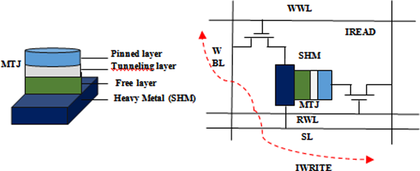
(a) SOT MRAM device architecture (b) Schematic of SOT-MRAM.
Biasing conditions of SOT-MRAM bitcell
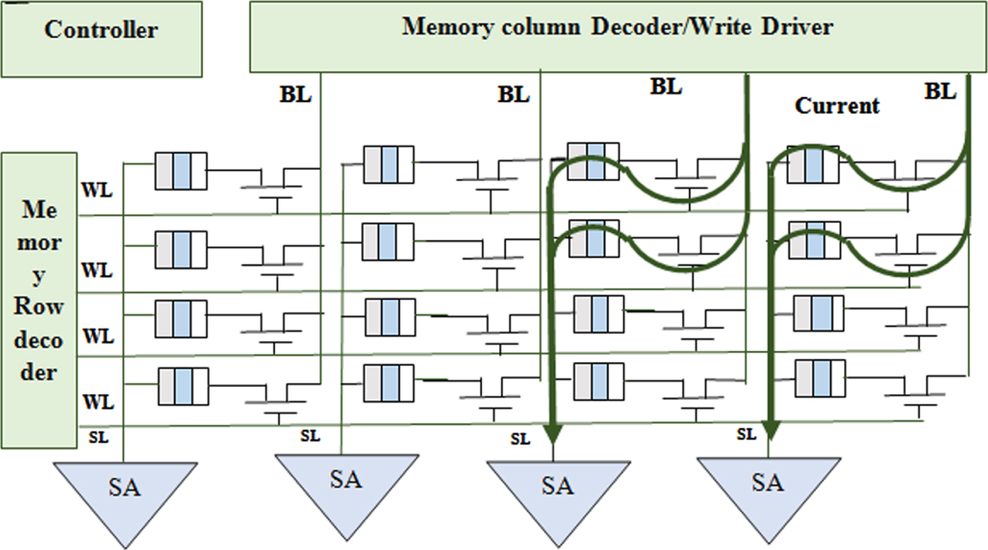
The SOT-MRAM sub-array architecture that is being shown could operate in a dual mode that can carry out memory read-write as well as AND/OR logic operations. To carry out standard memory operations, each SOT-MRAM cell was connected to the Write Word Line (WWL), Write Bit Line (WBL), Read Word Line (RWL), Read Bit Line (RBL), and Source Line (SL). Additionally, any two cells in the same column might be sensed concurrently in this system to carry out an in-memory logic function. The activation of the current path through the array is controlled by the peripheral decoders. The WBLs are utilized with voltage drivers to supply the necessary write voltage.
Memory Write: Write current must be injected through the SOT-heavy MRAM’s metal substrate in order to write a bit in either of its cells, such as the first row and first column. While keeping the remaining source lines and word lines disabled, the row decoder will enable WWL1 and ground SL1 for activating this write current path. The voltage driver (V1) linked to WBL1 is now adjusted to negative (/positive) write voltage in order to write a "1" (or a "0"). As a result, the MTJ resistance is set to High - R p (/Low - R p ), permitting for adequate charge current to proceed from V1 towards ground (/ground towards V1)
Memory Read: When reading data from a memory, a read current move from a chosen SOT-MRAM cell towards ground, producing a sense voltage at the SA’s input which is then compared towards the memory mode reference voltage (V sense , P < V ref < Vsense,AP). The enable values (EN M , EN AND , EN NOR )= (1,0,0) should be set to this reference voltage generation branch. Now, the outcome of the SA generates a low (/high) voltage signifying logic "0" (/"1") if the path resistance is lesser (/greater) than R ref , i.e. R AP (/R p ).
Computing Mode: Each pair of bits kept in the similar column could be simultaneously chosen as well as sensed throughout this mode. It should be noted that the row decoders have been updated to allow the multiple line enable function by integrating two single line enable decoders and connecting their outcomes to the OR gates. After that, SA differentiates the equivalent resistance of these parallel-connected SOT-MRAMs.
The SA can carry out fundamental Boolean operations (i.e. AND and OR) by choosing from a variety of reference resistances (EN AND , EN M , EN NOR ). R ref would be set at the intersection of R AP //R P (‘1’,‘1’) and R AP //R P (‘1’,‘0’) during the AND operation. Thus, the output becomes higher only when the two chosen SOT-MRAM bit-cells are simultaneously in the anti-parallel state. Otherwise, the output remains low. Corresponding to above, R ref usually set at the intersection of R P //R AP and R P //R P for the OR operation.
The Adder Neural Network (AdderNet), a novel class of CNNs that offers a good trade-off among speed and accuracy, is the foundation of the proposed Binary Convolution Neural Network (BCNN). CNN is a machine-learning classifier that analyzes images to determine the likelihood that certain features belong to particular output classes. A CNN often has numerous convolutional layers, fully-connected layers (FC) and pooling layers. It should be noted that convolutions should be employed to construct fully layered structures in an identical manner.
The L1 norm is where AdderNet evaluates how comparable the features are in convolutional layers. Employing the L2 norm among the activation X and the filter F, traditional CNNs produce the convolution result Y, as shown by equation (1), where (c, h, w) are (Channel, Height, Width) and p, q, and r are iterator variables. The lightweight addition and subtraction operations used by AdderNet in place of the computationally demanding multiplications result in reduced power consumption and quicker speed than typical CNNs, as shown by equation (2).
The precise computation procedure is listed below. Assume that the initial storage locations for the input fmaps (I) and kernels (W) in memory are the respective image banks as well as kernel banks. In order to do batch normalization, which will ensure minimal information loss, inputs were initially sent to the process. The second step is the binary operation with the sign function that binarizes the normalised inputs and weights. The suggested CIM ARRAY is then given binarized inputs I(B) and weights W(B) to execute an in memory operation.
Each layer of CNN’s convolutional layer is revealed to collect a feature grouping in a multiple channel format as input (Input fmaps). It applies W through convolutions of high dimensions, and then generates the output fmaps (features) for the following layer. The results will then be processed using a non-linear activation function, for instance, ReLU.
It is possible to fully perform the convolutional operation of I(B) and W(B) in memory by expressing it as follows:
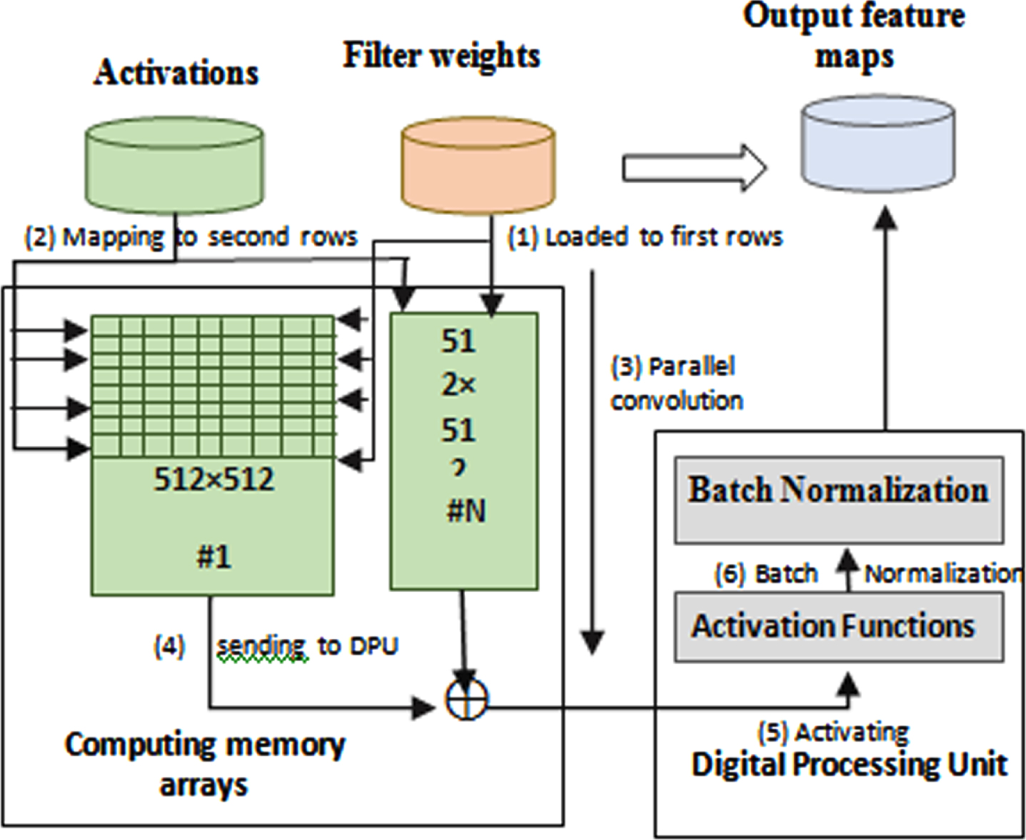
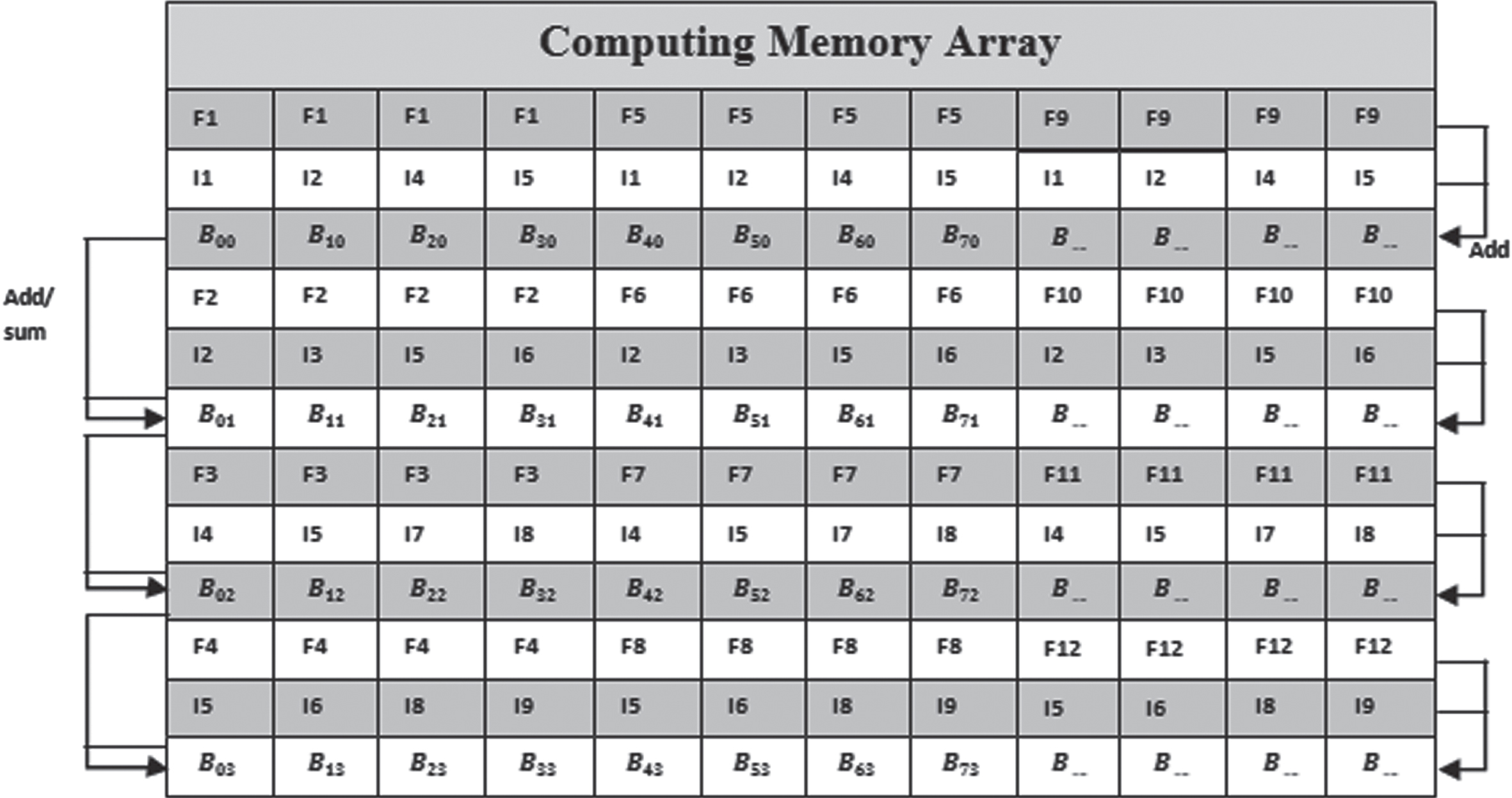
According to Fig. 2, the suggested BCNN is made up of computing memory arrays (CMAs) and data processing units (DPUs). The CMAs, which are outfitted with the suggested BCNN for adder’s sparse addition and subtraction operations, were under the control of convolutional and FC layers. It has 128K 2-bit weight registers, 4096 CMAs, and 64 MiB of total memory. The batch normalisation as well as the activation layers are handled by the DPU. With the exception of the lack of a hardware quantizer, the proposed DPU design is virtually identical to that of Para PIM and MRIMA.
The computation workflow of ABCNN.
Workflow of memory controller.
The weight quantizer is not essential because the weights of newer BCNNs are already quantized because they are taught to be 1-bit binary values. Due to the lack of a quantization mechanism, eliminating the quantizer also results in a reduction in chip space and power. In conclusion, the DPU, with its activation functions as well as batch normalization, cooperates with the CMAs with effective addition and subtraction.
Batch-normalization
By normalization of the input sample, it possess a zero mean with unit variance and decreases the information loss. The transformation could be defined as:
And the associated output and input pixels, respectively, are identified as I_0 (R) and I_i (R). σ and μ stand for statistics obtained while in training mode, γ as well as β indicates the parameters which were trained, and ɛ was used to avoid round-off issues. Every pixel of the input fmap is efficiently fetched by the DPU, which then writes back the matching normalized pixel because all the variables in the above mentioned equations are saved in SOT-MRAM sub-arrays.
Activation Function: The accuracy of network prediction is significantly influenced by the choices of the activation function. For maximum accuracy, this unit could be modified to conduct two different activation functions, notably (i.e.
Workflow: Convolution layers are handled by the CMA, and the other two tasks are undertaken by the DPU. The CMA is divided into odd as well as even rows, each of which can hold an 8-bit value. The odd rows are being provided with weights first. The activations should then be mapped to the even rows. Third, the convolution outcomes are calculated concurrently across all memory columns. The DPU then receives the convolution outcomes from each CMA. Fifth, the DPU activates the convolutional results using activation functions. To create the output feature maps, the DPU then performs batch normalisation and scales the normalised values into 8-bit numbers.
AdderNet In-Memory Convolution: By converting the activations to an Image-to-Column (Img2Col) fashion, it performs convolution in the General Matrix Multiplication (GMM) style. A GMM among Img2Col and the unrolled filters can be used to reconfigure the two-dimensional convolution with three filters, as shown in Fig. 4. Figure 5 displays the entire AdderNet workflow inside the CMA. The filters were duplicated at specific times to meet the shape of the converted activation, and they were mapped towards the first rows of the memory. The Img2Col, which are replicated for each filter, are stored in the second row. For purposes of illustration, the third row also serves as the even row. In order to record the partial sums that were immediate in the even rows, initially add together the associated values in every two rows. Second, determine if the accumulation of the partial sum requires addition or subtraction by reading the sign bit row. In order to perform addition/subtraction among the two partial sums and save the instantaneous value in the second operand, the Memory Controller (MC) then transmits the appropriate signals.
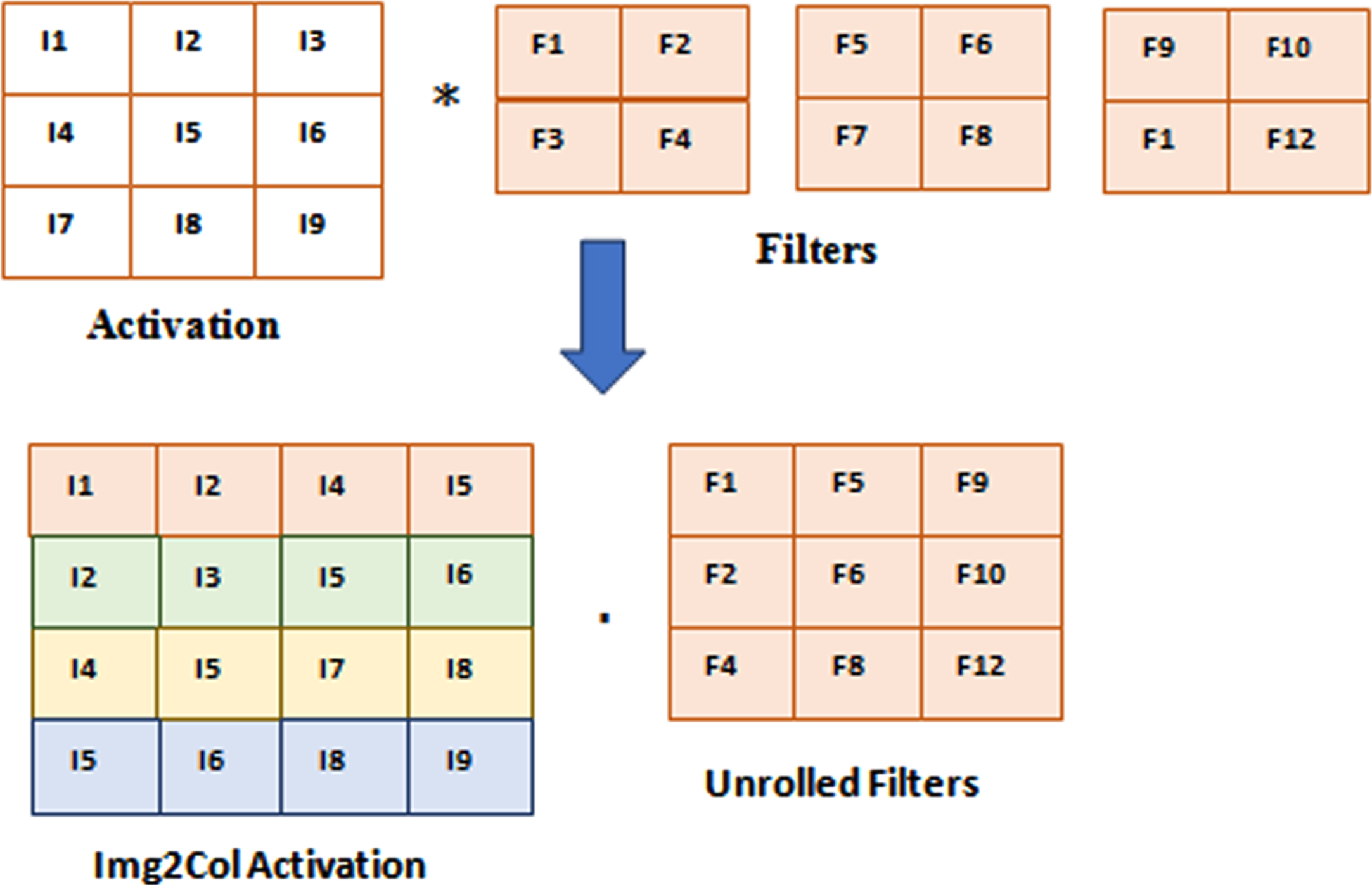
An Img2Col example.
GEMM dependent AdderNet convolution.
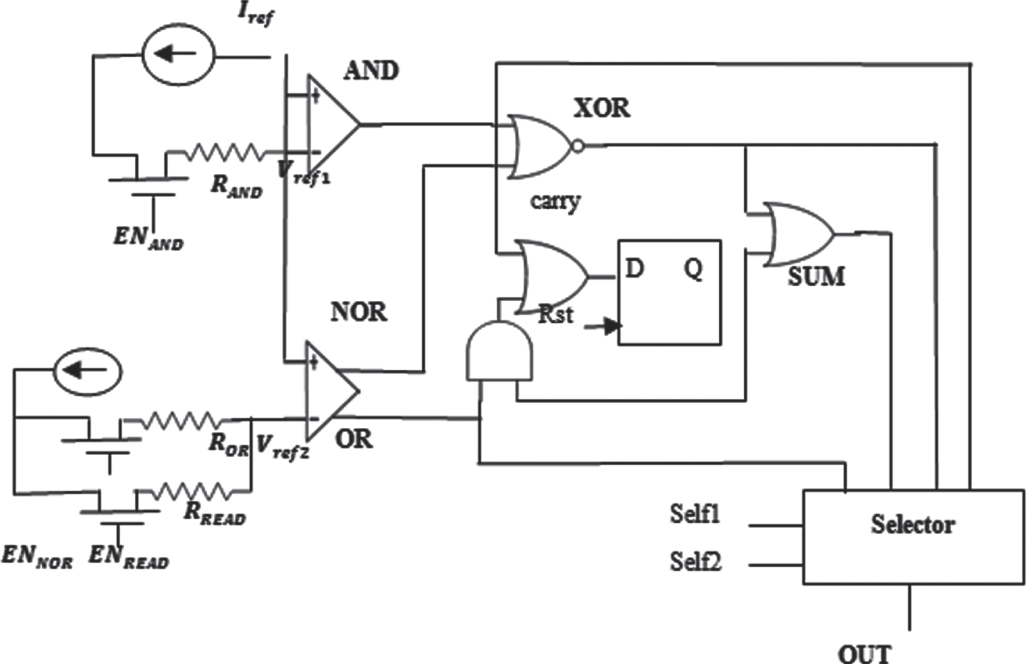
The SA architecture.
The MC then re-does the second action until the bottom of the column has the total accumulation outcome. Because every column has a SA, all of the columns are computing concurrently, which are the reason IMC devices perform well.
Sense Amplifier: The SA, which specifies the kind of operations the device can handle, is the essential part of an IMC device. In order to facilitate addition operations more rapidly and effectively than existing works, a SA must be designed. Additionally, the suggested SA is not only capable of the addition operation but also typical Boolean operations including subtraction. The SA performs READ, NOT, AND, NAND, OR, XOR, and Addition (ADD) functions natively and Subtraction (SUB) extensively.
Architecture and Workflow: Fig. 7 demonstrates the architecture of the recommended SA. Four phases contribute up the SA’s signal flow.
(a) The equivalent circuit for simultaneous two memory cellssensing. (b) The VREAD for single memory cellsensing. (c) The VAND and VOR for two memory cellssensing.
Sensing: According to equation (6), where I
ref
indicates the reference activation current and R
MTJ
indicates MTJ’s resistance as well as R
T
symbolizes the resistance of access transistor in the memory cell, the operational amplifier (OpAmp) in the SA collects the overall current from SL as well as the voltage of the SL V
SL
.
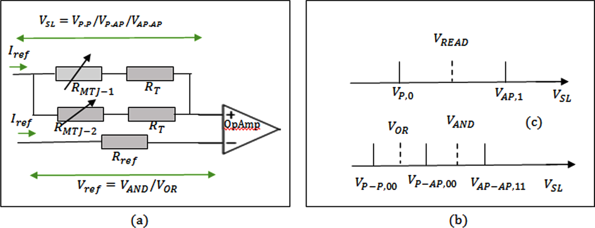
Comparing: The OpAmp in the SA receives the sensed voltage VSL and relates it to the reference voltages Vref . (provided in equation (10)) to produce the AND, READ or OR result, which may then be utilized to calculate more sophisticated functions. While reading out a solitary memory cell, the detected voltage VSL could alternatively be lesser (VP,O).
As demonstrated in Fig. 8(b), the reference voltage for reading V
READ
therefore lies within VP,O and VAP,1. Corresponding to this, as illustrated in Fig. 8(c), the sensed voltage VSL of reading out two memory cells could indeed be VP - P,00, VP - AP,01 and VP - AP,11. As a consequence, whereas the reference voltage for ANDV
AND
stands within VP - AP,01 and VP - AP,11
,
that of VOR is between VP - P,00 and VP - AP,01
.
Combining: In order to calculate complex functions, such as SUM and XOR, as well as carry out addition operations, as illustrated in Fig. 7, the various logic gates available in SA integrate the AND, NOR, and OR signals produced by the OpAmps. Equation (8) represents signals delivered by the OpAmp from the comparison step and illustrates how the XOR is computed, for instance, by NOR among the AND and NOR of operands A and B.
In a similar manner, equations (9) and (10) are employed to estimate the SUM and Carry-out C out , whereas C in symbolizes the Carry-in, saved in D-Latch. Consequently, as demonstrated by equation (11)–(13) and Fig. 7, the SA necessitates four logic gates (NOR, OR, AND and XOR) as well as one D-Latch in the combining phase.
Selecting: The desired outcome is then transmitted to the output port OUT by the selector depending on the selecting signals Sel1 as well as Sel2 as in Tables 2 and 3.
Selector signals configuration in the SA
Enable signals’s configuration in the SA
The recommended SA depends on the MC ’s enable and selector signals to produce the intended outcome. This modifies the SA’s enable signals so that it can serve various purposes. In the process, it chooses the outcomes sent to the selector’s input ports, and then receive the outcome at the OUT port.
Although the SA enables 8 functions, implementing 8 selection ports for each function adds complication and costs a lot of space. In order to minimize the design to just four selector ports, it optimizes the SA on the NOT, READ, SUB and NAND functions. First, because they both employ the same OpAmp, the OR and READ operations use the identical OR selector port. Second, since equation (11) demonstrates that NOT equals XOR with "1"s, thus it read in the operand combined with the row of "1"s and output the NOT outcome at the selector port of XOR. Third, when calculating the NAND at the SA’s second OpAmp, it turn off the EN READ and EN OR. When the VSL is larger than zero, the OpAmp NOR port outputs a "0". Equation (12) demonstrates how the NAND outcome follows a NOR between the AND and "0"s at the XOR port. Lastly, conduct the SUB operation through one NOT proceeded by one ADD as given in equation (13).
As a consequence, among the works currently in existence, the SA seems to have the fewest enabling (EN), selector, as well as amplifier signals.
When running AdderNet on IMC, the two bottlenecks were seen. First, compared to the addition operation, the two-step subtraction has a longer delay. Second, IMC platforms do not effectively utilize AdderNet’s absolute function. In order to increase performance, it performs two optimizations on the first AdderNet convolution. First, as shown by equation (14), it add to the subtractions found inside the absolute function. The filter weights F can be treated as constants and their opposite integers can be used in the L1 norm because they are known before inference. The absolute function’s subtractions are now added more effectively than before. Second, as shown by equations (15) –(16), it merge the accumulation with the Neg () function in place of the absolute function and eliminates the subtraction outside of the accumulation.
Equation (17) displays the overall number of operations performed by a single original AdderNet convolution layer. Without operator fusion, the ABS operator equals βSUB Equation (18) defines the operation number for the optimized AdderNet convolution. In contrast to the original, the optimized computation pipeline minimizes 2βSUB and improves βADD. Assuming β = 0.5, the optimized AdderNet eliminates 33% of subtractions and converts the remaining 33% into additions.
Testing on MNIST data set, Modified CACTI [11] as well as NVSim [12] are employed to evaluate the suggested accelerator’s system-level performance, speedup, and energy efficiency. Meantime, this utilizes existing technologies [13, 14] that perform comparisons utilising RRAM and SOT-MRAM. Following were the findings that contribute. The power and latency results are obtained from Virtuoso ADE L using Spretre, and the area is calculated using Virtuoso Layout L.
The proposed system refers to [15] for the write time of the 1-Transistor-1-Junction MRAM memory array implemented in the same 45nm process. Keeping the standard STT-MRAM array which accounts for around 85% area in a CMA unchanged, and modified the SA.
Performance of sense amplifier
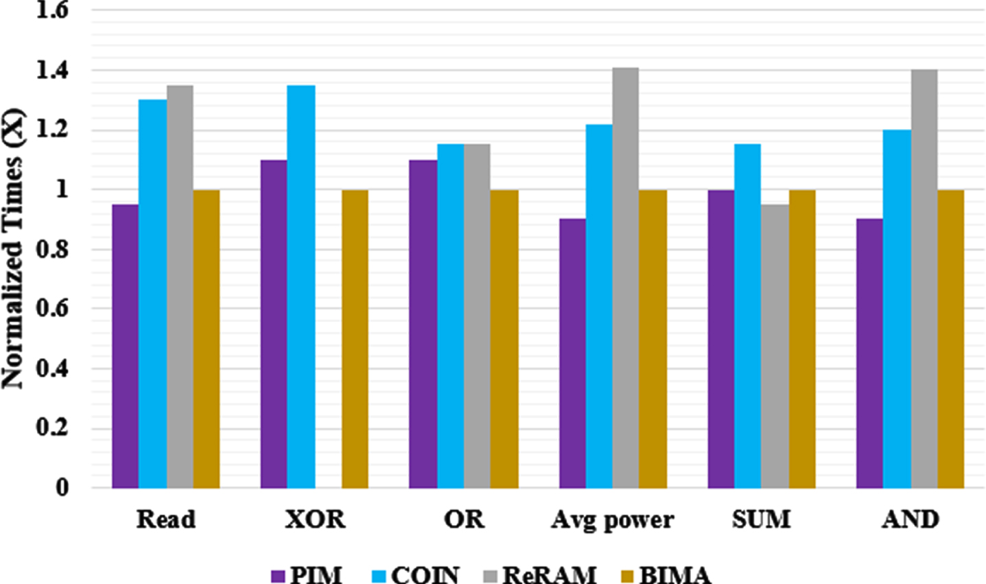
Power and Latency of In-Memory-Computing Operations: The performances of IMC in different SAs are compared, including PIM [16], COIN [17], ReRAM [18] and the proposed BIMA. The SUM, Read, OR, XOR and AND operations’ normalized CP latency and average dynamic power are depicted in Fig. 8.
Efficiency and latency of addition comparison.
From obtaining the sensing signal flowing from the memory cells until receiving the operation outcome at the OUT port, the SA latency has been estimated. PIM and BIMA both seem to have slightly shorter read latency than one another (14% for SUM and 15% for AND, OR, and XOR). The suggested BIMA outperforms ReRam on Read by 35% and on AND and OR by >15%. Owing to its aggressive processing technique, COIN outperforms FAT on SUM by 7%, however it would not support XOR. Additionally, the suggested BIMA has power efficiency gains over PIM and COIN of 1.32× and 1.51×, respectively.
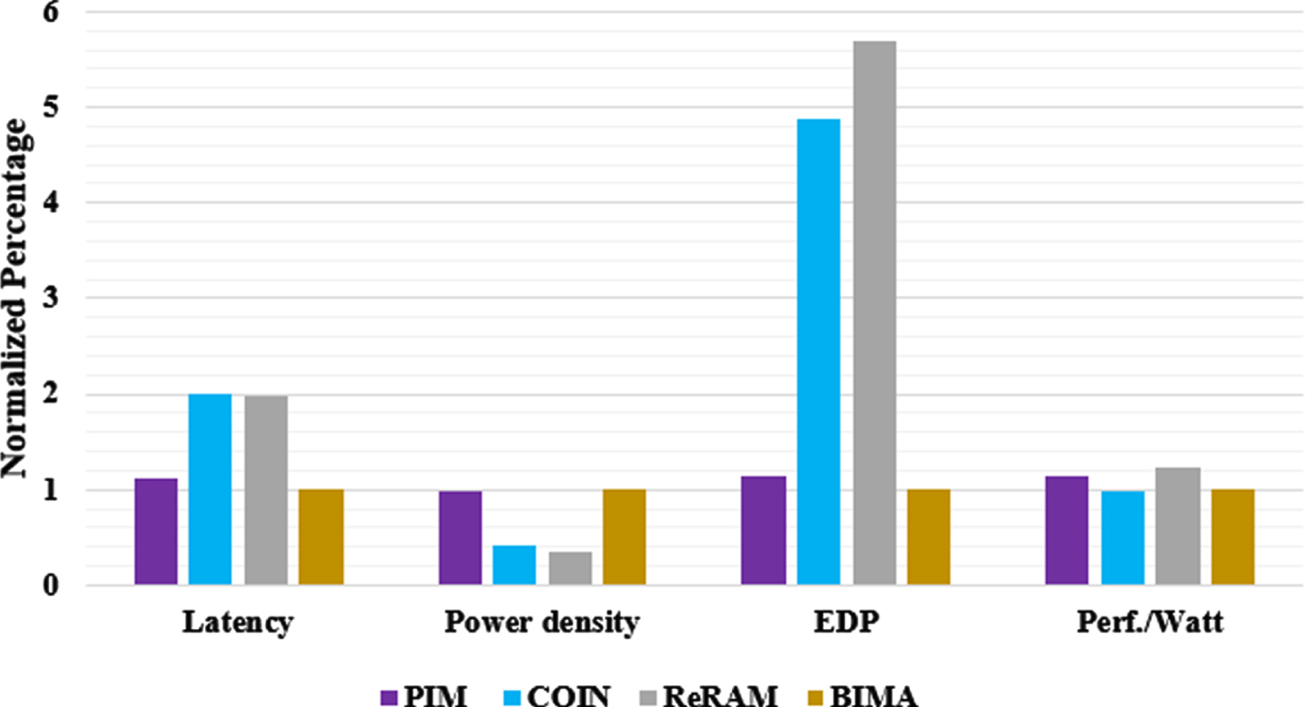
The PIM has the shortest critical path (CP) as well as the lowest latency when performing one scalar addition [19–21]. According to the SA and the suggested efficient addition strategy that accumulates the carry in a latch rather than the memory array, the proposed BIMS outperforms COIN and ReRAM in the CP, single addition, and vector addition. The effectiveness of these SAs was additionally examined in Fig. 9 along with the latency, Energy-Delay-Product (EDP), performance/watt, and power density (PD) in power/area.
Normalized area breakdown of the SA comparision.
First, BIMA is 1.14×, 3.14× and 3.36× faster than PIM, COIN and ReRAM respectively. When the additional write of Carry is taken into consideration, it is discovered that COIN and ReRAM are significantly slower than PIM [22–26]. Although writing the Carry onto the memory consumes a longer time, the addition as a whole had been slowed down even if ReRAM possesses lower processing delay in the SA. Thus, the BIMA has the shorter latency in addition. Second, BIMA had the largest performance/watt and is 1.12-2.976× as compared to the other works. Third, the proposed method has the lesser EDP among the existing works PIM, COIN and ReRAM. Fourth, BIMA possesses a reduced PD than PIM and ReRAM, which indicates that the proposed BIMA is more balanced to endure a longer lifetime.
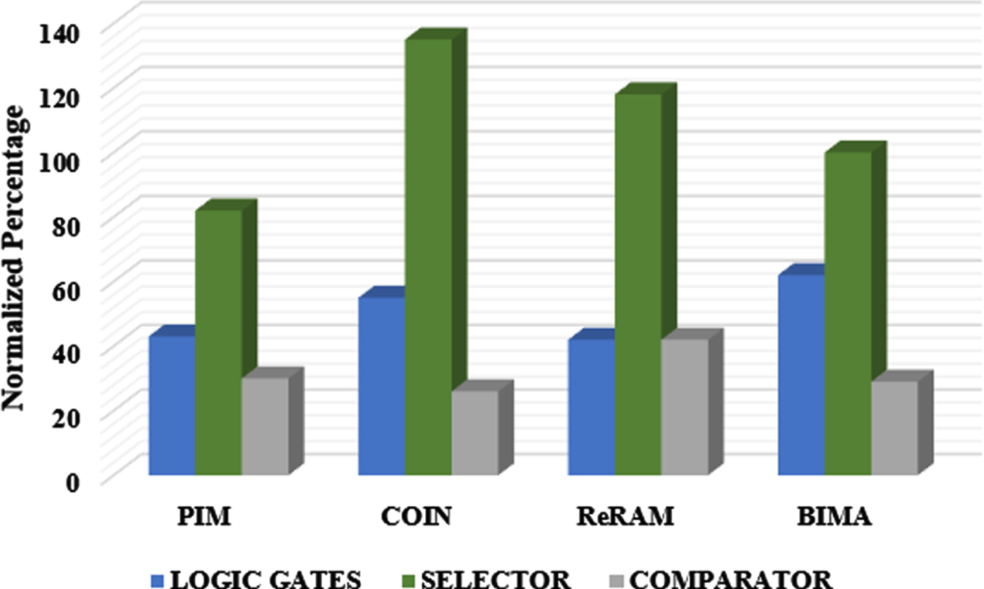
Reliability and Area of SA
The area of the proposed BIMA and associated works were illustrated in Fig. 10. Though BIMA comprises of the majority of logic gates, BIMA has lesser area than COIN and ReRAM. Also, the SA is more reliable than COIN and ReRAM. The sense margin of the two operand was 2.5× high, while comparable towards the three-operand operations. As a higher sense margin delivers lower error rate, the proposed SA is highly reliable comparing to PIM and ReRAM.
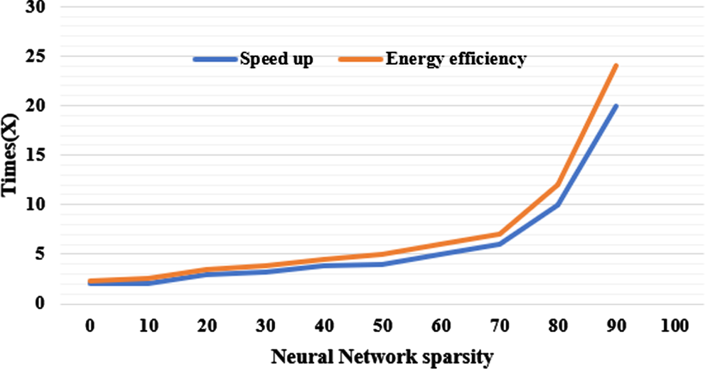
Energy efficiency and speedup of the BIMA across network sparsity.
On configurations with equivalent layer-to-layer sparsity, Fig. 11 demonstrates the network level speedup as well as energy efficiency, which further replicates the single layer parameters [27–30]. Although only PIM designs constitute BWN IMC accelerators within the three relevant works, PIM is employed as the baseline. The proposed accelerator could achieve 17.13× speedup and 18.20× efficiency compared with PIM.
Energy efficiency and speedup of the BIMA across network sparsity.
This research proposes a SOT-MRAM-based Binary CNN In-Memory Accelerator (BIMA) to minimize the power consumption and proposes an In-Memory Computing (IMC) for AdderNet convolution to further enhance the performance. And observe that the constraints on IMC are the replaceable subtractions as well as the inefficient absolute function. This performs comparable operator replacement as well as operator fusion to deliver an IMC-friendly AdderNet convolution, where the 1/3 subtractions are transformed to additions. and eliminates other 1/3 subtraction operations. Relying on the evaluation outcomes, the proposed accelerator outperforms the existing in-memory accelerator in terms of speedup and energy efficiency by 17.13 and 18.20, respectively.