
Abstract
Technological advances in the semiconductor industry and the increasing demand and development of wearable medical systems have enabled the development of dedicated chips for complex electroencephalogram (EEG) signal processing with smart functions and artificial intelligence‐based detections/classifications. Around 10 million transistors are integrated into a 1 mm2 silicon wafer surface in the dedicated chip, making wearable EEG systems a powerful dedicated processor instead of a wireless raw data transceiver. The reduction of amplifiers and analog‐digital converters on the silicon surface makes it possible to place the analog front‐end circuits within a tiny packaged chip; therefore, enabling high‐count EEG acquisition channels. This article introduces and reviews the state‐of‐the‐art dedicated chip designs for EEG processing, particularly for wearable systems. Furthermore, the analog circuits and digital platforms are included, and the technical details of circuit topology and logic architecture are presented in detail.
Keywords
1 Introduction
The electroencephalography (EEG) acquisition technology has been developing for several decades. Technological advances and improved scalability in semiconductor technology have enabled the replacement of discrete components with tiny integrated circuits. Furthermore, the application of EEG is increasing in number with increasing functionalities. EEG electronics have evolved from the simple electrodes‐amplifier-oscilloscope connection for a display to the acquisition by cable connected computer. Currently, wearable systems with artificial intelligence (AI) based self‐learning computation and adaptivity are becoming a trend in medical/commercial EEG products. Big tech companies such as Apple, Google, and Samsung have marketed commercial products and actively researching and designing solutions to promote the next‐generation of wearable brain–computer interface (BCI) [1]. Although medical information can be obtained from the human body, neural activity has gained more attention because it can provide a direct BCI. Consequently, providing novel practical applications beyond biomedical, such as collection and analysis in brain research, industrial control, and gaming.
As shown in the Fig. 1 in Ref. [1], a complete state‐of‐the‐art wearable EEG system can have the following key components that facilitate the EEG flow.
(1) The analog front‐end (AFE) amplified the analog‐digital conversion during EEG acquisition. The programable gain amplifier (PGA) amplifies the weak EEG signals from the electrodes with tunable gain based on the impedance and noise condition at the contact interface between the scalp and the electrodes.
(2) The digital core (DC) is a logic platform chip capable of processing a huge amount of raw EEG data from the high‐count channels of the AFE module. Consequently, the DC module outputs are processed and computed feature vectors, which significantly saves energy because less data is needed to be transmitted by the wireless module. The critical power and energy requirement of a wearable system defines the complexity of its digital part. Implementing the processing step directly on the wearable system is an energy‐efficient technique that reduces the power consumption associated with data transmission. Nevertheless, depending on the computational paradigms, feature extraction and classification of the signal may require complex algorithms. If not efficiently implemented and executed on high‐end hardware, the algorithm may fail to satisfy real‐time timing enclosure or consume too much energy in portable battery‐operated devices [1].
(3) The wireless communication between the wearable system and the main computer is often implemented using commercial energy‐efficient Bluetooth Low Energy (BLE) system on chip (SoC) such as Nordic nRF52832, to conserve power. The AFE and BLE modules consume significant power in the system, especially with unprocessed raw EEG data. In this condition, the BLE module keeps streaming data to the main computer in active mode, with power consumption reaching up to over 15 mW. As explained in (2), this condition can be improved by upgrading the computation capability of the DC module with ultra‐low‐power logic architectures. Consequently, the streaming time can be reduced by 91% as only computed featured vectors are transmitted.
In this review, we have selected state‐of-the‐art designs with technical advantages for an in‐depth introduction. They are classified into chips and programable devices and belong to AFE and DC modules. Section 2 introduces selected analog circuits in different types for neural recording (acquisition). Section 3 presents advanced energy‐efficient digital system chips with relatively high computational power for EEG signal processing with detection and classification functionalities. Section 4 provides the analysis and comparisons of the entire system.
2 AFE circuits in recent EEG chips
2.1 Circuits overview
Similar to the Fig. 1 in Ref. [1], the Fig. 1 in Ref. [2] shows the top‐level block diagram of a typical wireless EEG system for seizure/behavior detection and stimulation. It includes multiple recording and stimulation channels and neural signal processing units. The circuits we focused on consist of neural recording front‐end and neural stimulation circuit. The system has neural feature extraction and coding units, a wireless transceiver and transmitter, and a power management block.
Multiple channel analog signal conditioning circuits, including amplifying and provisional filtering circuits, are usually integrated into the neural signal acquisition front‐end. A multiplexer for time‐division multiplexing is usually adopted for multiple recoding channels to share the analog‐to‐digital converter (ADC). Similarly, the digital‐to‐analog converter (DAC) is shared by all the pulse generation channels in the neural stimulation module. On‐chip implementation of the signal processing unit, including feature extraction and neural coding, is important for reducing the wireless data rate and support the real‐time closed‐loop operation. Wireless transceiver and power management modules are widely used in EEG system designs to address device size and power transmission, two critical issues in wearable and portable close‐loop EEG system implementation.
2.2 Neural recording front‐end
The core blocks of the recording AFE include low noise amplifiers and PGAs. Neural signals are usually characterized by small‐signal amplitudes, easily buried in noise amidst large artifacts and stimulation transients. High‐level neural recording AFE poses great challenges in circuits design with higher precision, lower power, and smaller area, particularly for high‐density signal recording channels with stringent power and volume budget.
Generally, the amplitude of the raw neural signal ranges from multiple micro‐volts to milli‐volt. To achieve a sufficient signal‐to‐noise ratio (SNR) for the target signal, the total input‐referred noise of the neural recording AFE should be lower than 1 μV (rms), and the common‐mode rejection ratio (CMRR) should be higher than 60 dB [3]. Furthermore, the neural tissue is accompanied by a large DC offset at different electrodes. The DC offset typically varies between several mV and tens of mV. It can go up to a maximum of hundreds of mV, leading to a high‐gain neural recording amplifier’s saturation.
Different state‐of‐the‐art designs for neural recording AFE have been published in recent years. Several topologies implement the AFE design with the trade‐off between noise, offset, and gain, including AC‐coupled AFE, DC‐coupled AFE, and ADC‐direct AFE.
2.2.1 AC‐coupled neural recording AFE
Recording low‐frequency neural signals while rejecting the tissue DC offset usually requires the neural amplifiers with a small neural high‐pass pole. AC‐coupling capacitors associated with diode‐connected MOS pseudo‐resistors are widely used in the neural recording AFE to block the input DC offset [4 –7]. This method’s representative circuit architecture is shown in the Fig. 6 in Ref. [4] and the Fig. 4 in Ref. [5].
In these AC‐coupled AFE designs, capacitors in parallel with a MOS pseudo‐resistors in the feedback loop are commonly adopted to generate a high‐pass pole. Therefore, the input DC offset is blocked by large AC‐coupled capacitors, and closed‐loop gain is determined by the capacitor ratio at the feedback loop and input capacitors. Based on this topology, the high‐pass frequency and gain neural recording amplifier can be tuned by changing capacitors’ value at the input and feedback loop.
One of these designs’ disadvantages is the large input capacitors, which occupy a significant silicon area in the EEG chip, making it unsuitable for high‐density neural signal recording channels. Furthermore, large input capacitors may decrease the equivalent input impedance of the neural recording AFE; therefore, degrading the CMRR performance of the whole system. The input capacitors at the differential input cause mismatching. This approach may lead to additional circuits for input impedance boosting and ripple cancelation;
consequently, significantly increasing the silicon area and power requirement [6, 7].
Another disadvantage of these designs is that the MOS pseudo‐resistor in the feedback loop exhibits non‐linear behavior in the presence of a large output voltage swing and the DC operating point drift due to process, voltage, and temperature (PVT) variation. This non-linearity may cause large signal distortion and makes the high‐pass pole frequency time-variant [4]. Two diode‐connected MOS transistors with adjustable gate voltages are implemented in the second stage’s feedback loop to improve the linearity performance of the neural AFE [8]. The results showed that low‐frequency distortion and drift could be effectively mitigated. However, large input capacitors are required, which degrade the system performance, including CMRR and input impedance.
2.2.2 DC‐coupled neural recording AFE
Due to the AC‐coupled input challenges in the neural recording amplifier design, DC‐coupled input is increasingly gaining attention in recent years [9 –12]. As a preventive design, a low‐pass filter in the feedback network is used to block the DC offset, where the DC voltage at the output of the preamplifier is sensed and subtracted from the input to provide a high‐pass filter. As shown in the Fig. 1 in Ref. [9], to remove the low‐frequency noise of the biopotential signal, an analog integrator with a large integrating time‐constant in the feedback loop in the front‐end amplifier is applied [9]. However, the same issue caused by the non‐linear pseudo‐resistor in the feedback has not been completely resolved, as discussed earlier. Furthermore, this design cannot achieve good noise and CMRR performance due to the single‐end configuration. Moreover, two signal chains with the proposed configuration are required for differential electrodes input, leading to mismatching.
As a revised topology, a passive RC LPF is used in the feedback loop, and a differential difference amplifier (DDA) is utilized to cancel the DC offset of the signal, as shown in the Fig. 3 in Ref. [12]. The DDA with a small high‐pass pole cancels the signal’s low‐frequency and DC portion by feeding them back through the second differential pair. The main drawback of this topology is that the passive elements are too large to be integrated into a single chip, which is not suitable for small chip area design and integrating more signal acquisition channels.
Reference [13] presented a hybrid structure implementation through the feedback network by employing a digital LPF to achieve low current consumption and an additional analog LPF to reduce the dynamic range of the DC offset. With this methodology, the requirement of DAC resolution is relaxed, and the DC offset is rejected. The disadvantage of this architecture is as follows. First, the complicated design with two different filter types in the feedback path for one preamplifier design increases the area and power consumption. Second, noise subtracted by the digital filter operation will degrade the total noise performance of the preamplifier. Third, this structure is implemented using only a sing‐end input. Differential input makes this design more complex and can lead to other design issues, such as mismatching.
Based on the above discussions, a fully‐digital feedback network could be a powerful solution, enabling complex and flexible operation behaviors in the digital domain; therefore, achieving higher performance. References [10] and [11] presented a digital feedback circuit to block the DC offset and low‐frequency noise interference. Usually, digital filters and DACs are used in the feedback. Large capacitors or pseudo‐resistors are not required in the digital feedback loop, enabling control of the circuit’s behavior with more flexibility and accuracy. However, the experimental results showed that the input‐referred noise and CMRR performance are degraded with the large input offset. The degraded performance is partly due to the substrate noise introduced by digital modules in the mixed‐signal designs.
2.2.3 ADC‐direct neural recording AFE
A new design methodology based on the ADC‐direct approach is presented in Ref. [14] to address the design challenges, such as noise, power, and area for integrated neural recording AFE. As shown in the Fig. 4(a) in Ref. [14], the neural recording AFE includes a hybrid analog/digital second‐order oversampling ADC with predictive digital auto‐ranging. This design is characterized by a high input dynamic range and rapid transient recovery. The neural signal is directly coupled to the system with high conversion gain, noise, and dynamic offset that can be canceled by digital processing in the digital domain. Based on this design, neural conditioning circuits such as high‐pass filtering and amplification are not needed in the signal recording path, which usually cause signal distortion. However, the design’s main drawback is that the complicated design of second‐order oversampling ADC for each channel increases the area and power consumption of the neural recording system, which is not suitable for multi‐channel applications. Furthermore, sampling noise enters directly in the system without attenuation, which degrades the system’s noise performance.
3 Digital processing in recent EEG chips
3.1 Circuits overview
EEG signal processing is an important step for the whole system. Specific processor architectures with tailored circuitries for signal processing and computation are the trends in existing wearable EEG systems. In the detailed main flow of calculation, for different applications, we need to process the EEG signals differently in both the scalp and intracranial EEGs seizures manifest as a redistribution of spectral energy on a set of channels [15]. For each channel, the EEG signals should be transformed into the spectral domain to get spectral features. Another method is to use fast Fourier transform (FFT) to perform frequency analysis on EEG signals with higher spectral resolution besides digital filters. The support vector machine (SVM) is considered an efficient method for detecting seizure/behavior. The SVM module can perform a fast and energy‐efficient classification with high sensitivity by using spectral features from multiple channels on‐chip or off‐chip to train the SVM model running on suitable well‐designed chip circuits. Convolutional neural network (CNN) is another alternative for classification with more powerful computation for multi-classification but higher complexity in silicon area. We selected several state‐of‐art digital core chip designs (processor‐based mainly) for advanced EEG processing with high computation power, representing possible future digital core trends in wearable systems.
3.2 Time‐frequency conversion
The first important step in digitized EEG signal processing is the time‐frequency domain conversion. Besides the conventional digital filtering by transforming raw EEG data into specific bands for detection and classification. The combination of real‐valued fast Fourier transform (RFFT) and complex‐valued fast Fourier transform (CFFT) is a novel method in recent hardware design. In Ref. [16], a 512‐point RFFT is implemented via a 256‐point CFFT by using CFFT‐to‐RFFT conversion. A delay line composed of 256 registers in the last stage, which accounts for 50% of the overall memory usage, can be waved. Figure 8 in Ref. [16] shows the architecture for the CFFT‐to‐RFFT converter.
First, the design converts the fixed point (FP) 256‐point CFFT outputs into floating‐point (FLP) representation to achieve the accuracy required for subsequent feature computation. Second, coordinate rotation digital computers (CORDIC) are used to implement trigonometric functions based on add‐and‐shift operations.
FLP arithmetic is adopted to improve hardware efficiency. A 24‐bit FLP format is chosen in Ref. [16], including an 18‐bit mantissa and a 6‐bit exponent. Figure 7(c) in Ref. [16] shows the FP‐to‐FLP converter in the CFFT‐to‐RFFT converter. For a 2’s complement value, the FP‐to‐FLP converter converts the most significant bit in the mantissa (not the sign bit) by finding the leading one in the exponent shift data. This architecture partitioned the comparison in 8‐bit in parallel to reduce the critical‐path signal propagation. Given the same numerical accuracy, the proposed FLP circuit achieved a 20% reduction in area and saved 11% power compared with the direct‐mapped 38‐bit FP design.
3.3 Feature extraction
In EEG signal analysis, the spectral‐energy distribution is the key element for analysis in seizure detection and emotion classification without human judgment. It is mainly accumulated and normalized from the energy calculation of different bands or FFT outputs.
The normalized spectral‐energy feature F can be computed from the energy E for the i th sub‐band given by Eqs. (1) and (2) [16].
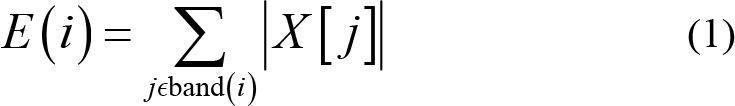
Unlike accumulating the results from FFT in Ref. [17], in Ref. [16], the energy is normalized to suppress the value variation; therefore, building up a faster and more accurate classification. The Fig. 9 in Ref. [16] shows the hardware‐shared spectral‐energy computing unit. The values of the RFFT in Eq. (1) is computed by a CORDIC using the circular vectoring mode. The square‐root calculation in the denominator of Eq. (2) can be processed by sharing the same CORDIC in the circular vectoring mode. The equivalent hardware is capable of calculating the related division in the linear vectoring mode.
Figure 9 in Ref. [16] shows the CORDIC‐based processing element (PE), including the exponential function calculation by utilizing an FLP CORDIC. Furthermore, the PE can be modified to compute the required functions, such as vector rotation for eigenvalue decomposition and exponential operation for the SVM kernel function.
Extracting only spectral‐energy features is not enough when using a BCI system in other applications other than seizure recognition. Such as sleep stage classification, spectral edge frequency (SEF) is also an important feature. SEF works by comparing the sum of calculated powers in a specific band against a given threshold. The threshold is computed by multiplying the given band’s total power by the required percentage (edge) [17].
In Ref. [18], CNN is applied to recognize emotion. The feature extraction engine formats the six collected raw EEG data from specified channels into one EEG image. The image contains emotional information using tailored filters, short‐time Fourier transform (STFT) to involve the frequency information, and differential asymmetry (DASM) for the asymmetrical information. In addition, a sample entropy (SE) calculation unit was integrated to automatically evaluate the left‐right hemisphere channel pairs based on the specific subjects’ biased asymmetrical responses. The block diagram of the feature extraction engine that generates the EEG image used as CNN input is displayed in the Fig. 4 in Ref. [18]. The results of the SE unit were used to calculate two groups of weight values to carry out optimized channel reconstruction weighting based on whether the average SE value of the frontal channels was less than that of prefrontal channels. The DASM unit subtracted the STFT results for each channel pair and delivered the related results to the channel reconstruction unit.
3.4 Non‐linear SVM module
Extracted Features are used for further analysis in machine learning classification, where a decision will be generated by the chip. In recent research, the alternating direction method of multipliers (ADMM) has been used to solve linear SVM with feature selection. However, it is difficult to apply the ADMM algorithm to non‐linear SVM training for hardware implementation because of the need to use large‐scale matrices for optimization.
In Ref. [16], a highly parallel ADMM‐based algorithm is adopted to solve the non‐linear SVM training problem. The overall ADMM‐based algorithm with a rank approximation for non‐linear SVM training is summarized in the Algorithm 1 [19]. It transforms a non‐linear SVM training problem into a linear SVM training problem with a similar structure.
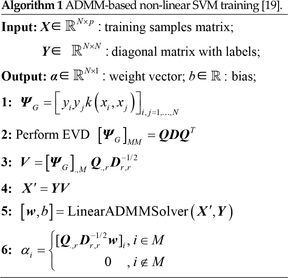
ADMM‐based non‐linear SVM training [19].
The ADMM‐based SVM training algorithm involves large‐scale matrix inversion, where the matrix dimension is related to the number of training samples. Generally, for seizure detection applications, the matrix size ranges from hundreds to thousands, making hardware implementation impractical. In Ref. [16], eight spectral‐energy features from each channel are extracted from the 3–26 Hz frequency band, generating 112 features for 14 channels, which will consume huge storage space. The mRMR feature selection algorithm was applied to reduce the feature vector dimensions.
The mRMR algorithm in Ref. [16] picks up the features that have the closest relevance
3.5 Decision trees
Human sleep is broadly classified into five phases: REM, Wake, N1, N2, and N3. In this case, according to the application that requires multiple classifications, CNN or decision trees are technically better choices to solve such problems than SVM classifiers.
In Ref. [17], sleep staging algorithm using decision trees have been implemented in hardware. Figure 2 in Ref. [17] shows the main flow of the sleep staging method. When the system detects sleep stage change, a group of one‐versus‐one decision trees is applied to issue the new stage. The decision trees, their step of execution, and the features required are firmly based on the current sleep stage and the likelihood of the next one.
For example, the system starts at the Wake stage. If the newly extracted features have changed, the system will perform classification decisions in a specific order (depends on the last stage). It is an implementation of the finite state machine approach. The simplicity of this type of method is that sleep classification only requires to compare the features to thresholds.
3.6 Entire processor‐based digital platform
All the above modules and general calculation circuits like specified multipliers, adders, CORDIC circuits, and multiply‐and‐accumulation units in EEG processing and analysis, can be integrated into a monolithic silicon chip as a programmable elaborated processor for wearable BCI systems. Several state‐of‐art physical implementations have been published with improved logic architectures for massive computation of classification, online training in machine learning, or energy‐efficient purposes.
3.6.1 SVM‐based processor for epileptic seizure control
In Ref. [16], the SVM processor has 3.76 M gates fabricated on an area of 2.55 mm2, based on the 40‐nm CMOS technology. Table II in Ref. [16] shows the performance of the stateof‐the‐art seizure detector chips. The Table reveals that the design of Ref. [16] has high sensitivity while maintaining low detection latency, which is unattainable by other designs. Although the design in Ref. [20] has low detection latency, the sensitivity is very low compared to the designs tested on the famous CHB‐MIT database. The design in Ref. [16] has the highest sensitivity performance of 96.6% and a low FAR of 0.28/h based on 24 subjects through on‐chip learning. Even though Ref. [21] has a much lower energy per operation, its function is much simpler than Ref. [16] as the online self‐learning and programmability are not included. The Fig. 16(a) and (b) in Ref. [16] are the die photo of the chip and summary.
3.6.2 Emotion recognition system chip using CNN
In Ref. [18], the tailored CNN chip was implemented in TSMC 28‐nm CMOS technology and was tested using the Agilent 93000 SoC platform. In the paper, the authors have proposed “a multiphase CNN execution method to accommodate hardware resource constraints. Datasets of 32 subjects from the DEAP database were used to validate the proposed design, exhibiting mean accuracies for valance binary classification and valance‐arousal quaternary classification of 83.36% and 76.67%, respectively”. The core area of the chip was 1.83 × 1.83 mm2. The power consumption measured in the training and testing modes were 76.61 mW and 29.5 mW, respectively. Table III in Ref. [18] shows the comparison. The average accuracy of the binary classification and the quaternary classification derived from the multidimensional model in Ref. [18] was 83.36% and 76.67%, respectively, higher than other studies. Figure 19 in Ref. [18] shows the die photo of the chip, and the Table II in Ref. [18] gives the related summary.
3.6.3 Chip for automatic sleep staging
The sleep staging SoC in Ref. [17] is taped out based on the AMS 0.18 μm process technology featuring six metal layers. The total chip area with the AFE involved is 10.3 mm2. The SoC power supply scheme is simple using a sole 1.25 V supply, and its mean power consumption is 575 μW, working with a clock frequency of 1.5 kHz. As it is the first fabrication of an all‐flow sleep staging algorithm on‐chip, it is hard and inapplicable to make direct comparisons of its performance with those of other different systems that have been developed for different targets application. However, the power dissipation of the design is much lower. The Table IV in Ref. [17] shows the comparison of related works published in recent years. Figure 11 in Ref. [17] shows the die photo of the system chip, and the chip summary is listed in Table III in Ref. [17].
3.6.4 Multi‐core processor platform for general-purpose wearable BCI system
An energy‐efficient wearable system for general BCI “BioWolf” was presented in Ref. [1]. The BioWolf features three main components, including a well‐designed parallel ultra‐low power defined SoC MCU for signal processing, a Nordic ARM‐SoC MCU for BLE communications and interface management, and an AFE for bio‐signal acquisition from Texas Instruments.
The processing core of the BioWolf system is based on a PULP SoC called Mr. Wolf. Mr. Wolf is a high‐count core configurable platform fabricated in TSMC 40‐nm CMOS technology, cooperating with a 12 K gates RISC‐V processor communicating with peripherals and optimal power management, with a parallel combination of eight RISC‐V processor cores facilitated with adaptable and powerful DSP extensions, especially the floating‐point units. Therefore, the system can handle a huge computation of raw EEG data. Moreover, only calculated features and classified results are needed for streaming by the BLE module instead of streaming a large amount of raw data. Consequently, the battery’s energy is conserved as the BLE is not required to work all the time during the system’s operation.
The average overall and trial accuracy of the BioWolf system are 0.82 and 0.95, with a mean output latency of 1.26 s. The average information transfer rate is above 1.4 b/s. The power requirement is about 6.31 mW, ensuring up to 38 h of battery life. A summary of the tailored chip for BCI processing is shown in the Table II in Ref. [1], and the die photo is shown in the Fig. 4 in Ref. [1].
4 Conclusion
EEG BCI technology has evolved based on technological advancement in semiconductor technologies. Currently, a general size chip can execute complex algorithms for advanced EEG signal processing and huge computation. The scaling of the number of transistors on a wafer and the optimization of operating voltage makes the SoC energy‐efficient and portable. The parallel logic architecture and ultra‐low power techniques help achieve the implementation of such complex chips. Furthermore, there are two main trends in recent EEG chip designs with different methodologies for specific purposes.
On the one hand, all the modules of an open/close‐loop EEG systems are integrated into one monolithic chip based on specified semiconductor technology, an SoC scheme. The entire system is relatively small as all the main functions are integrated into a single chip, and the PCB board is tiny, which improves wearability. Although power and energy consumption can be reduced significantly, the cost and stability may be affected by the natural difference in analog and digital circuits requirements, including frequency response, mode of inputs, SNR, and the PVT variations. It is difficult to implement analog and digital circuits on one silicon substrate because the supply voltage, process, and noise margin requirements are different. Notably, the large on‐chip capacitors of analog circuits can significantly increase the cost of producing the chip if fabricated using expensive and advanced technology. The cross‐communication between the analog and digital circuits is another disadvantage of the SoC scheme. SoC‐based wearable systems for EEG processing is small in size and fast. However, its price and stability are probably not attractive in the commercial market.
On the other hand, the analog and digital parts are separated. However, combining well‐designed analog and digital chips is implemented on suitable technologies with efficient energy supplies and without expensive cross‐communication. The submicron process handles the large area capacitors with economical cost and satisfies the relatively‐high I‐V requirements of analog circuits. Furthermore, the nano process provides fast and reduced transistor switches to build up high-performance logic architectures for the digital platform inside a tiny single chip. The high‐cost process is used to integrate maximum transistors to facilitate processing functions, while economic technology is used to fabricate amplifiers or ADCs with strong driving current strength. The overall energy efficiency, production cost, and stability are better than the SoC scheme with a slightly bigger wearable system.
The chiplet design has become the focus of the integrated circuit area; a fully integrated module with fabricated dies of analog and digital cores for EEG processing is potentially the future trend of wearable systems. Unlike the SoC design, the chiplet method focuses on the single package of all the fabricated chip dies of analog and digital circuits, based on different suitable processes. Micro bonding between these chip dies help connect analog and digital parts efficiently in the micron range without implementing them on one silicon substrate in one process. In this method, the wearable system’s size can be reduced as all the discretely packaged chip dies are packaged together while avoiding the SoC scheme’s challenges. We expect more AI‐based elements can be integrated into a small long‐battery‐life wearable EEG system in the future with powerful functions in processing, classification, and smart detections.
Footnotes
Conflict of interests
The authors declare that they have no conflict of interests.
Acknowledgement
This work was supported by the National Natural Science Foundation of China (Grant No. 61974095), the Natural Science Foundation of Guangdong Province, China (Grant No. 2018A030313169), the Foundation for Young Talents in Higher Education of Guangdong (Grant No. 2018KQNCX405), and the Natural Science Foundation of Top Talent of SZTU (Grant No. 2019010801004).