
Abstract
Electron microscopy has undergone a major revolution in the past few years because of the practical implementation of correctors for the parasitic lens aberrations that otherwise limit resolution. This has been particularly significant for scanning transmission electron microscopy (STEM) and now allows electron beams to be produced with a spot size of well below 1 Å, sufficient to resolve inter-atomic spacings in most crystal structures. This means that the advantages of STEM, relatively straightforward interpretation of images and highly localised analysis through electron energy-loss spectroscopy, can now be applied with atomic resolution to all kinds of materials and nanostructures. As this review shows, this is revolutionising our understanding of functional oxide ceramics, thin films, heterostructures and nanoparticles. This includes quantitative analysis of structures with picometre precision, mapping of electric polarisation at the unit cell scale, and mapping of chemistry and bonding on an atom-by-atom basis. This is also now providing the kind of high quality data that are very complementary to density functional theory (DFT) modelling, and combined DFT/microscopy studies are now providing deep insights into the structure and electronic structure of oxide nanostructures. Finally, some suggestions are made as to the prospects for further advances in our atomistic understanding of such materials as a consequence of recent technical advances in spectroscopy and imaging.
Introduction
In recent years, a whole range of fascinating phenomena have been found in oxide materials, or their surfaces or interfaces. These include among many others:
novel electric transport properties at heterophase or internal interfaces 1–11
unusual magnetic phenomena at heterophase interfaces 5,12–14
stabilisation of unusual phases and resulting novel properties in oxide thin films 15–17
construction of new morphotropic phase boundaries in a wide range of ferroelectric materials 17–20
creation of multiferroic oxides combining permanent magnetic and polarisation orderings 21–25
control of bulk properties through interface chemistry. 26
These are just a few examples from a vibrant field, and for a more comprehensive review, the interested reader is referred to the review of Martin et al. 27 and the references therein.
Many of these achievements depend on phenomena arising at the atomic scale and therefore atomic-resolution characterisation of the structure and chemistry is essential to a full understanding of the origins of such phenomena. Such atomic-scale structural and chemical characterisation has become possible in recent years because of major advances in scanning transmission microscopy arising out of technical advances in the correction of the lens aberrations in the probe-forming lenses. This article will show how such advances are being applied to allow major insights into the structure, chemistry and behaviour of functional oxides. First, a brief outline of the essentials of aberration-corrected STEM (AC-STEM) is provided, specifically for the benefit of non-microscopists. The applications of AC-STEM to functional oxides is then reviewed including in imaging of atomic structures of materials, interfaces and nanoscale defects; atomic-resolution spectroscopy of the chemistry of thin films, heterostructures, interfaces and defects; and in situ studies of materials. Consideration is then given to future developments in AC-STEM and their relevance to the science and technology of functional oxide materials, nanostructures and devices.
Aberration-corrected STEM: brief history
Since the invention of the electron microscope by Knoll and Ruska 28 back in the 1930s, electron microscopes have been widely used in understanding the microscale and nanoscale structure of materials and for most of the history of transmission electron microscopy, it has been the classic broad-beam techniques pioneered in Ruska and Knoll's instrument that have been dominant in science. Nevertheless, even back in the 1930s, Knoll 29 and von Ardenne 30 were both experimenting with scanning a fine probe of electrons across a specimen and assembling an image in a serial fashion. This technique fell out of favour and only really came back to the fore in the 1960s and 1970s with the work of Albert Crewe at Chicago, 31,32 and the use of ultra-high vacuum chambers, cold field emission guns (CFEGs) for electrons, and the introduction of annular detectors led to a massive step forwards. Perhaps, the culmination of this was the imaging of single heavy atoms with the Chicago STEM. 33 Following this development, several companies including Hitachi, AEI, Siemens and Vacuum Generators (VG) started to produce commercial CFEG dedicated STEMs and these were installed in a number of laboratories. These found particular application in high spatial resolution electron energy-loss spectroscopy and energy dispersive X-ray spectroscopy of materials. 34 Nevertheless, transmission electron microscopy continued to be dominated by broad-beam techniques, and with a few notable exceptions, the majority of electron microscopy laboratories concentrated on TEM, although many institutions had STEM-capable TEMs mainly intended for use on analytical studies.
The revolution came in the mid to late 1990s. It had been known for years from the work of Otto Scherzer that in electron microscopy, geometric distortions of the wavefront because of spherical and chromatic aberrations were inevitable in conventional round electron lenses, 35 in particular because there are no diverging round lenses for electrons (unlike the situation for visible light, where aberration correction is much simpler). Scherzer made important contributions in understanding the resolution limits in conventional lenses, maximising the resolution available from conventional lenses (the well-known Scherzer defocus 36 ), together with proposals for aberration correction. 36,37 This spurred a sustained effort to develop a practical aberration corrector, not only in Scherzer's group 38–40 but also elsewhere. 41–43 The two main schemes proposed have used combinations of multipole electromagnetic lenses (either quadrupole–octupole-, or multiple sextupole-based designs 43 ) to create an effective compound lens with an overall negative spherical aberration. Sadly, most of the earlier attempts at practical realisation of an aberration-corrected microscope, while theoretically sound, failed not only on the grounds of electrical or mechanical stability but also because of the lack of automated alignment schemes (as computers were of course not readily available). In the 1990s, Zach and Haider managed to realise a working practical implementation of aberration correction in a scanning electron microscope, 44 based on a corrector design by Rose, one of Scherzer's former students. This was very quickly followed by aberration correction of the objective lens of a transmission electron microscope 45 and the achievement of 1 Å and better resolution in high-resolution TEM (HRTEM) at conventional accelerating voltages of 200 kV. 46,47 Parallel developments by Krivanek, Dellby and Lupini led to the correction of the aberrations in the probe-forming lens of a STEM, 48 and this was retrofitted onto a number of VG STEM instruments (one of the first going to the SuperSTEM laboratory). It was very quickly demonstrated that this led to a dramatic jump in the achievable imaging resolution of STEM from generally worse than 2 Å to significantly better than 1 Å. 49 This had a dramatic and immediate scientific impact, in that atomic structures of many materials could now be easily resolved. When observing crystalline materials aligned to a specific zone axis, the contrast in typical annular dark-field (ADF) STEM micrographs allows a relatively straightforward interpretation of images in terms of atomic positions, where a bright spot is an atomic column, almost irrespective of sample thickness. 50,51 In the intervening decade since these early AC-STEM instruments were introduced, further developments have been made in instrumentation to make instruments easier to use, to improve the sample mounting and ease of tilting, and to better couple spectrometers to the microscope to allow for efficient collection of spectroscopic signals. All major transmission electron microscope manufacturers now produce aberration-corrected STEM instruments. As will be discussed later, the ease with which such spectroscopy can now be performed with resolution right down to the atomic scale is revolutionising our understanding of the nanoworld. The result is that, from the situation in the mid 1990s where most transmission electron microscopes sold were principally broad-beam TEM instruments, possibly with a STEM capability as an add-on, we are now in a situation where the majority of new installations in materials or physical sciences are now TEM/STEM instruments with excellent STEM capability, and very often aberration correction in the probe-forming optics. Moreover, STEM is becoming the standard technique for nanoscale or atomic-scale materials analysis. In view of this complete shift in approaches over just a few years, it is appropriate that we take time to review the effects of this shift in just one important field of materials science and technology: functional oxides.
Basics of STEM
We will first take a short space to review the basic principles of STEM including imaging and spectroscopy, in a simple, descriptive and non-mathematical fashion for the benefit of the non-specialist reader. The schematic layout of a STEM is summarised in Fig. 1, in the configuration used in the VG-style instruments with the electron source at the base (many TEM-based instruments from the established manufacturers use a top-down layout instead, i.e. inverted with respect to these diagrams). The probe-forming lens, which is shown here as one lens, although it will be a compound lens in a real microscope, acts to place a demagnified image of the electron source onto the specimen. In order to do this, the optical system is arranged so that the source is far from the lens and the specimen is very close to the focal point of the lens. The CFEG provides major advantages for STEM in that it provides a very small area from which the emission takes place. Thus, even without aberration correction, the demagnified filament image is very small and can be ∼2 Å. Additionally, since the CFEG is operated close to room temperature, the energy spread of the electrons because of thermal excitations will be small, and as a result any chromatic aberration in the probe-forming lens(es) will not have a disastrous effect on the probe formation. The principal limitation on how small this filament image can be made will come from geometric aberrations in the probe-forming lens system. Any and all corrections that can be made to the aberrations of this lens will therefore result in appreciable improvements in the resulting probe size. (Note: chromatic aberration becomes a more limiting effect at lower accelerating voltages, and efforts are underway to also correct chromatic aberration in next-generation instruments 52 ).
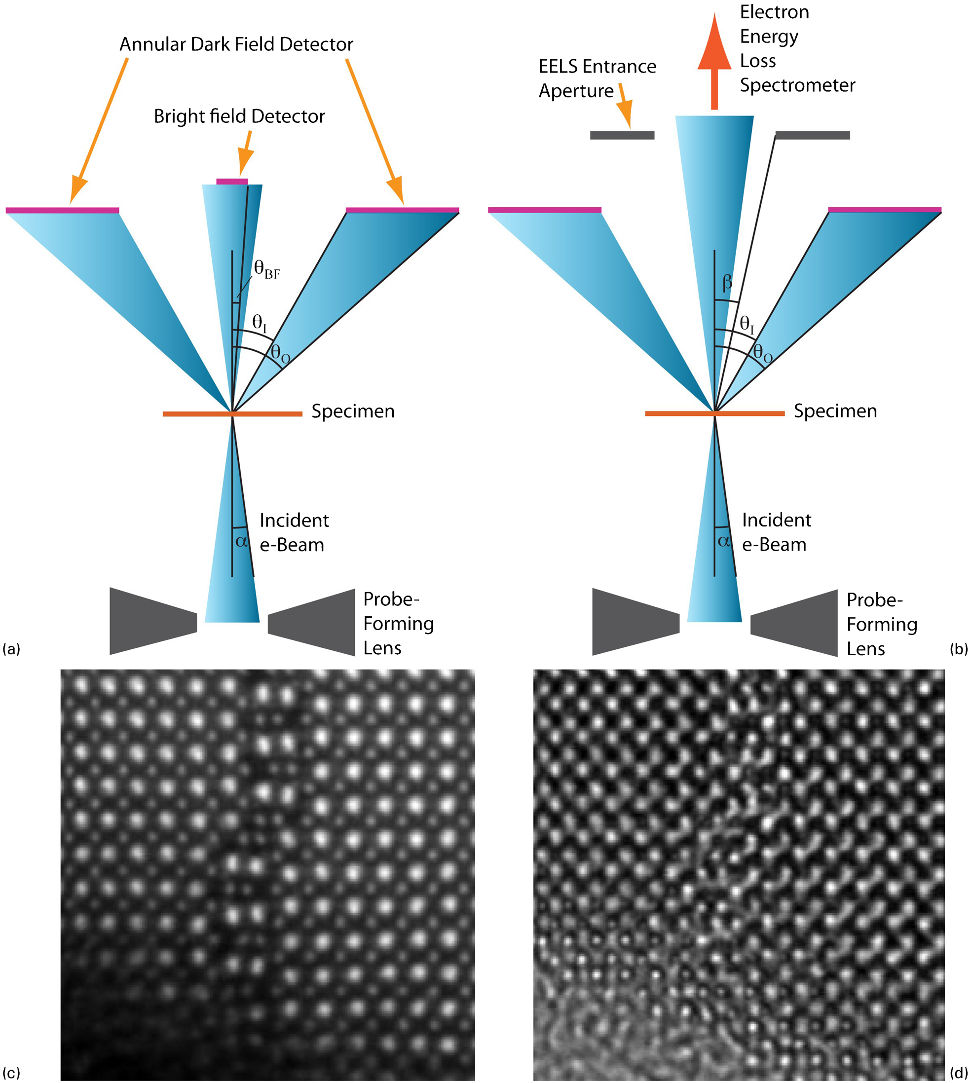
Schematic diagram of a scanning transmission electron microscopy (STEM) showing the probe formation geometry and some of the signals that can be collected: a setup for bright-field (BF) and dark-field imaging; b setup for electron energy-loss spectroscopy with simultaneous high-angle annular dark field (HAADF) imaging; c atomic-resolution HAADF image of an anti-phase boundary in a Nd-, Ti-codoped BiFeO3 perovskite ceramic (sample courtesy of Professor I. M. Reaney, University of Sheffield). Heavy cations appear as bright columns (the heavier, the brighter, intensity scaling approximately as the square of the atomic number), whereas oxygen columns are usually not visible; d BF image recorded simultaneously with c. Owing to the phase-contrast nature of the image, contrast inversions can be observed as the sample becomes thicker away from the edge. In the upper section of the image, the imaging conditions are such that oxygen columns appear as bright dots
Forming a fine probe on the specimen is critical to the recent success of STEM, but ultimately, all scanned microscopy still requires the collection of interpretable signals to form images; this is also summarised in Fig. 1.
One of the key developments that led to the success of the pioneering work of Albert Crewe was the introduction of ADF detectors. 31 Simply put, an ADF detector is an annular detector (usually a scintillator-photomultiplier detector) whose inner and outer angles (θI and θO) are defined both by physical dimensions and positioning in the column, as well as by any post-specimen projector lenses. The outer angle θO is typically very large (200 mrad or more), and only limited in practice by physical restrictions in the column (shadowing from the probe-forming lens assembly for instance). Depending on the inner angle, different mechanisms will then contribute to the signal arriving at the detector. If the inner angle of the ADF detector is greater than the convergence angle of the probe, then this will produce a dark-field image (i.e. vacuum appears dark). For inner angles only a little larger than the probe convergence, coherent diffraction effects provide a large contribution to the overall signal recorded by the detector, 53 which is then often referred to as medium (or low) angle ADF (MAADF or LAADF). For a typical probe angle α of 15–30 mrad for probe-corrected instruments, then an inner angle θI of 30–60 mrad would be appropriate for MAADF contrast. Such images have been more frequently used again in recent years: their contrast, while retaining some of the characteristics of high-angle ADF (HAADF) (no contrast inversion, interpretability of atomic columns over a large focus range, as discussed below), is also good at showing features that diffract strongly, e.g. strained areas such as dislocations, nanosized coherent or semi-coherent precipitates and the like. If the inner angle of the detector is set rather larger (e.g. θI = 80–100 mrad for a probe of convergence angle α = 30 mrad), then there will be little diffracted intensity on the detector, and the main source of electrons arriving at the detector will be from high-angle, incoherent, ‘Rutherford’ scattering of electrons by atomic nuclei. 54 This is strongly dependent on atomic number, varying as approximately Z 2 for isolated atoms. For this reason, this HAADF imaging has often been referred to as Z-contrast imaging. Of course, the situation in real samples may be a little more complex where the channelling of electrons along specific crystal directions may modify the scattering dependence from that of isolated atoms. Consequently, Z 2 dependence is not a safe assumption in all cases. The present authors would generally advise careful quantification and comparison with simulations to avoid mistaken interpretations. A good example of an atomic-resolution HAADF image is shown in Fig. 1c , which is of an anti-phase boundary in a perovskite, Nd, Ti-doped BiFeO3, viewed along a <001>direction of the primitive perovskite structure; in this image, the very heavy Bi atoms (Z = 83) are bright, the B-site cations (Fe and Ti) are weaker but still visible, and the oxygen atoms are not seen.
One signal that is straightforward to collect is the BF signal, which is simply recorded using a circular detector centred on the optic axis. The range of angles collected by this detector (0–θBF in Fig. 1) can either be determined by the physical size of the detector and its physical distance from the sample or can be adjusted by post-specimen projector system lenses. The contrast on this BF detector is, however, principally a phase contrast, especially at very low angles as BF STEM images can then be shown by reciprocity to be (almost) equivalent to BF images obtained on a conventional broad-beam TEM. As for HRTEM micrographs, the contrast is critically dependent on sample thickness and microscope defocus, and can show contrast inversions. For this reason, while quantitative use has been made of BF atomic-resolution STEM imaging, comparison with simulations is essential in all such studies to avoid false interpretations. An example of an atomic-resolution BF image is shown in Fig. 1d , which was acquired simultaneously with the HAADF image of Fig 1c . In this image, the oxygen atoms in the perovskite appear bright, and the Bi and Fe/Ti columns are dark, except in the very thinnest areas. It may also be noted in Fig. 1d that non-idealities in the imaging, such as slight local sample or beam tilt, have a much larger deleterious effect on the image than in an HAADF image; in this image, the imaging is almost perfect at the top, but there are more streaks and imaging artefacts in the lower part arising from a slight curvature of the sample close to the edge.
One related development of great note has been the recent renewed interest in so-called annular BF (ABF) imaging, 55,56 where an annular detector is used to collect the outer section of the BF disc (a small circular beam stop can also be placed so that it casts a shadow on the central part of the BF detector). While the inner part of the BF disc is dominated by phase contrast and is, as such, very thick and defocus dependent, work so far with the aid of simulations seems to show that the outer part of the BF disc produces images that are more incoherent and reveal all atoms as dark shadows, including light atoms such as oxygen 56 or possibly even hydrogen. 57
One of the great strengths of STEM is the large number of analytical signals that can be collected simultaneously with the acquisition of an HAADF and/or BF image: X-rays, visible light (through cathodoluminescence), secondary or Auger electrons, to name a few. Crucially, the BF detector can be also removed and the electrons collected into an electron energy-loss spectrometer, as also shown in Fig. 1; 58–60 the collection angle into the spectrometer is a key parameter and is conventionally denoted as β. The resulting electron energy-loss spectroscopy can now be performed at atomic resolution, 61,62 as will be reviewed for oxides later in this paper. Electron energy-loss spectroscopy is incredibly powerful for revealing information about chemistry, chemical bonding and electronic structure in materials, and is very efficient because almost all electrons passing through the sample are collected into the spectrometer.
Nevertheless, there are some elements for which the electron energy-loss spectroscopy (EELS) edges are difficult to separate from the background, especially when in the presence of another element with a strong edge preceding the edge of interest. For this reason, there are cases where X-ray spectroscopy is more suitable for certain elements or combinations of elements, and many STEM instruments will also be fitted with X-ray spectrometers. Unfortunately, X-rays can be emitted in any direction (i.e. 4π sr of solid angle) and it is not possible to build a detector that samples all of this 4π sr. The largest sampling commercially available at the time of writing uses multiple silicon drift detectors to offer about 1 sr (i.e. <1/12 of the total possible solid angle); more standard systems offer about 0⋅1–0⋅6 sr. Recent advances at the Argonne National Laboratory have resulted in the development of a π sr detector, 63 although this is not yet widely available. Thus, counting statistics in X-ray analysis with typical setups will have significant disadvantages over EELS, but nevertheless, this will be very powerful for certain elements or combinations of elements, provided sufficient time is allowed for analysis. Atomic-resolution EDX has been demonstrated, 64–66 but there has been limited use of this to date for the study of functional oxides 67,68 and mostly focussed on the methodology and not on the science of the functional oxides.
Whichever analytical technique is chosen, it is highly likely that to minimise beam damage and contamination on the sample, as well as to allow the collection of data from a reasonable area of the sample in as short a time as possible, the data are likely to be somewhat noisy. For this reason, post-processing of EELS or X-ray analytical data using statistical noise reduction techniques such as principal component analysis can be very helpful in separating the real signal from the random noise. 69
Application of AC-STEM to functional oxides
Atomic-resolution imaging and quantitative structure recovery
Earlier studies using atomic-resolution STEM imaging in oxides concentrated on using the unprecedented resolution to study materials with what was at the time unprecedented clarity, mainly using HAADF imaging. Examples of such studies include the work of Browning et al. 70 and McGibbon et al. 71 on grain boundaries in YBa2Cu3O7-x high TC superconductors and SrTiO3, respectively. In this work, qualitative matching of atomic-resolution images to theoretically predicted structures was used to verify the theoretical predictions. By contrast, the improvements in resolution and the extra sensitivity of aberration-corrected STEM instruments have enabled truly quantitative studies of atomic structures of materials, and this section will concentrate on such studies.
As stated above, a key advantage of combining the atomic resolution provided by aberration correction with the simplicity of contrast available using the HAADF imaging mode is that white spots in images of crystalline structures oriented along a specific zone axis usually appear exactly at the locations of the atomic columns. This means that the positions of atoms can be measured exactly. Moreover, as was realised first by the HRTEM community, for a pixelated image of an atom (or column of atoms), the centre of mass of an image of an atom can be located with picometre precision using two-dimensional (2D) Gaussian peak fitting; 72 i.e. the precision with which well-resolved atoms can be located far exceeds the resolution of the microscope. (The very same principle has been well used in super-resolution light microscopy in the biological sciences where the position of biological objects can be determined with a precision of a few nanometres using visible light and fluorescent markers. 73–75 ). The application of such quantitative approaches to STEM images has led in recent years to a flurry of work in which atom positions are now routinely measured with picometre precision and in which we have moved beyond simple qualitative matching of atomic structures to images into a new paradigm where structures are now determined quantitatively from STEM images. 17,76–87
Probably, the first published atomic structure quantification of a functional oxide using HAADF-STEM was carried out by Pyrz et al. on Mo–V–Nb–Te–O catalyst materials. 76 The issue at stake was that, while these materials are promising catalysts for selective oxidation in organic processes, it is difficult to have perfect confidence in Rietveld refinements of the structure from diffraction data because of the sheer number of possible adjustable parameters in such a complex structure. On the other hand, if such a structure could be well imaged using atomic-resolution STEM, then quantitative models could be constructed from extraction of the 2D coordinates of all atomic columns projected onto the image plane. The resulting structure model could then be compared to existing models or could be used as a starting point for new refinements. This is illustrated in Fig. 2, which shows an overlay of the structure model on the original HAADF image. Further work by this group examined other structures in the doped Mo–V–O system and then used the STEM results to challenge previous assumptions about structures determined using diffraction techniques alone. 79
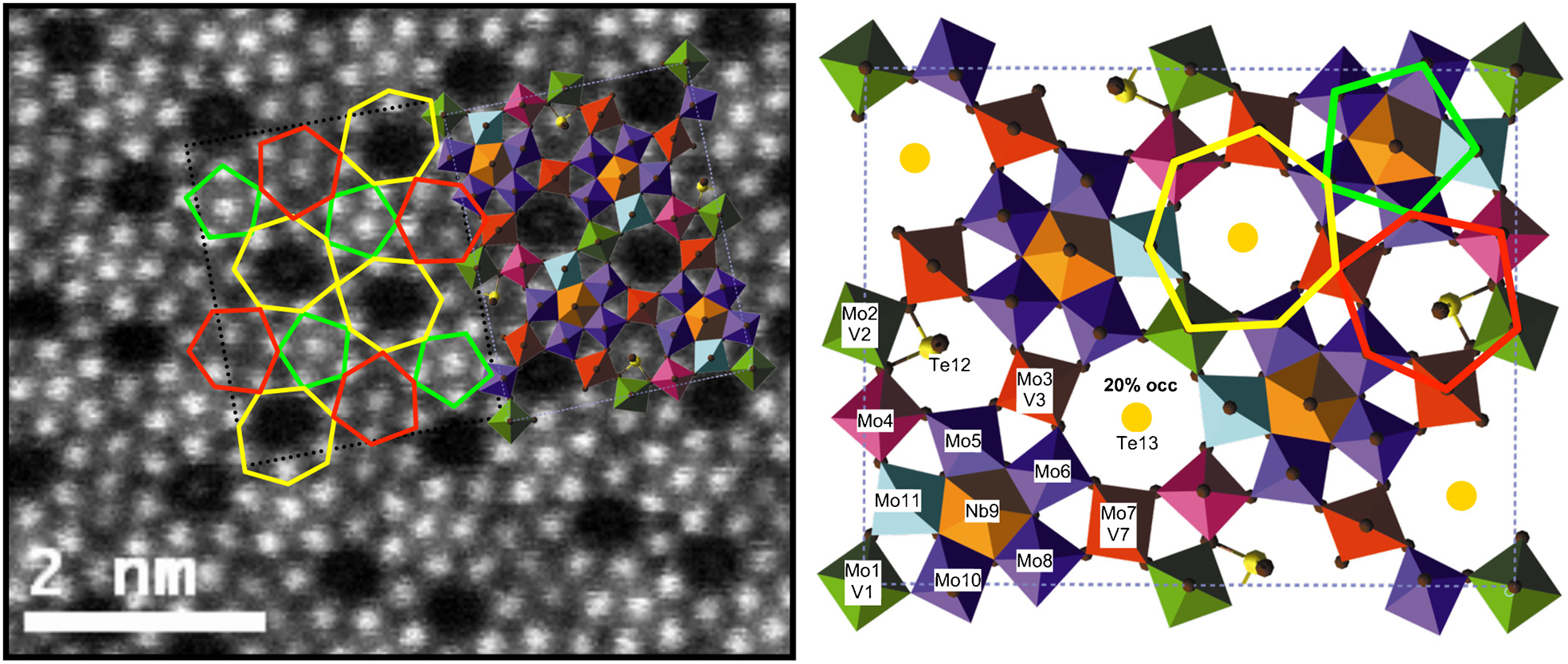
Structure determination of a complex MoVTeNbO phase using quantitative analysis of atomic-resolution high-angle annular dark field (HAADF) scanning transmission electron microscopy (STEM) images; the figure shows the original HAADF-STEM image overlaid with the structural model for the phase. The structural model is reproduced next to the HAADF image with all polyhedra (of Mo, Mo/V and Nb) labelled, as well as the fully and partially occupied Te channels. Reproduced with permission from Pyrz et al., 76 copyright 2008 Wiley-VCH Verlag GmbH & Co. KGaA, Weinheim
While STEM is a very valuable addition to the arsenal of techniques for studying complex bulk crystal structures, it really comes into its own when studying structures that are only present at the nanoscale. One such situation is ‘incommensurate’ structures occurring close to a phase boundary, such as that between the rhombohedral ferroelectric and orthorhombic anti-ferroelectric phases in Zr-rich Pb(Zr,Ti)O3. This system has been well studied, and diffraction patterns containing superstructure reflections along a 110 reciprocal lattice direction are often seen with a periodicity incommensurate with the primitive perovskite cell. 88–90 Nevertheless, the atomic-scale details of this system were only revealed by the application of quantitative analysis of AC-STEM images. 84 Particular care was taken to minimise drift effects and to measure and compensate any distortions of the data arising from imperfections in the microscope scanning system. This analysis revealed that the ‘incommensurate’ phase actually consists of patches with an eight-layer modulated structure and other patches with a six-layer modulated structure. The modulation of the Pb positions across these cells could be mapped and followed an approximately sinusoidal anti-ferroelectric pattern in both structural units, and this could be used to calculate the local polarisation across both new repeat units as summarised in Fig. 3. It was clearly shown that atom displacements and peak polarisations matched exceptionally well with those for the commensurate four-layer structure of PbZrO3. 91
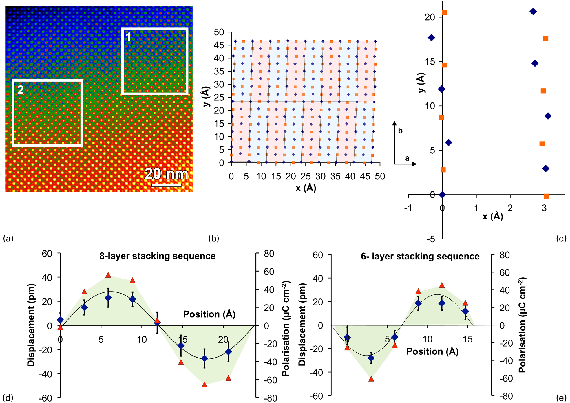
Pb positions and local polarisation mapping across the unit cell of two new anti-ferroelectric structures found using quantitative analysis of high-angle annular dark field (HAADF) scanning transmission electron microscopy (STEM) imaging of the ‘incommensurate’ structure of 4% La-doped Pb(Zr0⋅9Ti0⋅1)O3: a HAADF image of the structure; b identification of 16 repeat units in box
While quantitative atom position measurement is of huge significance in quantifying nanoscale structures, there is further interpretable information encoded in the intensities of the columns in HAADF images. As stated above, this is approximately proportional to Z 2 for free atoms, and is certainly strongly Z-dependent (although simulations would always be advised by the present authors). This has been used by Choi et al. 92 to quantify the substitution of La onto different A-sites in CaCu3Ti4O12. Similarly, this was used by Azough et al. to study ordering of vacancies on A-sites in La2/3TiO3–LaAlO3 ceramics. 93 Advanced image intensity analysis techniques based on statistical parameter estimation theory were recently developed by van Aert et al., 87 which even allow in certain cases for precise atom counting within an atomic column. It may be noted that Pyrz and coworkers also used column intensities to infer column contents in their work. 76,78
Moving beyond bulk materials, thin films are a particularly rich field of application for all techniques based on transmission electron microscopy, because while X-ray diffraction yields valuable information, giving a nanostructural context to explain the diffraction information is essential. This was clearly the case in the seminal paper of Zeches et al. 17 on the growth of thin films of bismuth ferrite on YAlO3 and LaAlO3. These substrates have a much smaller lattice parameter than the bulk lattice parameter of BiFeO3, resulting in a large compressive in-plane strain. Previous quantitative studies of similar compressively strained films of other perovskites (using HRTEM) had shown that structural changes and small tetragonal distortions of the film can happen under such conditions (e.g. MacLaren et al. 15 ), but what happened in this particular case was a huge surprise. Zeches et al. 17 found that the film adopted a complex domain structure with a mixture of distorted rhombohedral BiFeO3 (not unexpected) and a hitherto unknown supertetragonal BiFeO3 with a c/a ratio of ∼4/3. This resulted in a flurry of studies, both experimental investigations with further atomic-resolution imaging, 94,95 as well as theoretical calculations of alternate phases that can be stabilised in BiFeO3 under different constraints, 96,97 and all this was provoked by atomic-resolution AC-STEM imaging.
A feature of numerous studies since 2010 has been the use of quantitative position measurement of different types of atom in a crystal structure to allow the calculation of local polarisation at a unit cell level 83,84,86,98–101 following earlier work using HRTEM. 102,103 This has been used to reveal features like polarisation rotation at flux-closure domains in BiFeO3 thin films 98 as highlighted in Fig. 4, in a similar manner to comparable work performed using HRTEM on flux-closure domains in Pb(Zr,Ti)O3 thin films. 104 Polarisation mapping has also been used to identify polarisation rotation at domain boundaries. 100,101 It has also been used in understanding how interfaces in thin films and heterostructures affect local polarisation near the interface and has resulted in impressive correlation with theoretical calculations. 83,86 The majority of such studies worked with simple perovskite structures and used the displacement of the B-site ion with respect to the A-site ion as a measure of polarisation, although the recent work of Han et al. quantified local displacements associated with polarisation across domain boundaries in hexagonal ErMnO3. 105 Recent work, inspired by the HRTEM community, 102–104 has also quantified position of oxygen atomic columns using BF STEM imaging to include oxygen atom displacements in the polarisation calculations to give an even more reliable result. 106
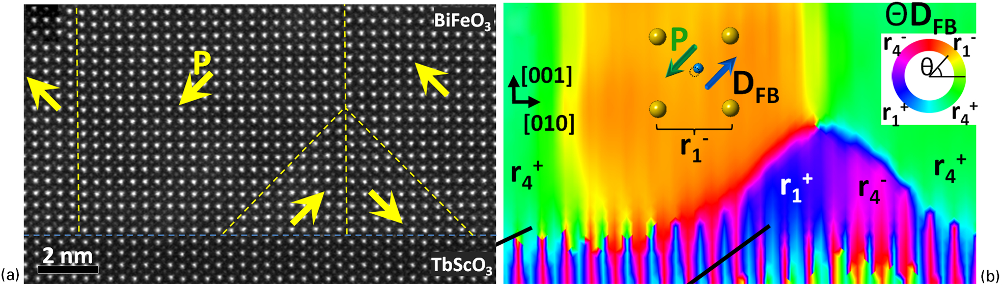
Polarisation rotation at flux-closure domains in a BiFeO3 thin film on a TbScO3 substrate from Nelson: a high-angle annular dark field (HAADF) image of the domain structure, with domain boundaries and polarisation directions superimposed; b a map of the direction of the displacement of the B-site cation with respect to the A-site cation determined from the image of a, which reveals the polarisation directions in the image. The BiFeO3 shows the polarisation rotation at each of the domain boundaries and the flux-closure pattern close to the interface of the substrate. The TbScO3 shows a characteristic vertical striped appearance because of a structure characterised by antiparallel A-site displacements in adjacent rows. Reprinted with permission from Nelson et al. 98 Copyright 2011, American Chemical Society
Buried interfaces both in heterostructures and within a single phase are, of course, objects where atomic-resolution electron microscopy is just about the only technique that will be able to probe and quantify the structure experimentally. The additional possibilities that have been offered by aberration correction have led to many significant advances in the understanding of interfaces and novel effects caused by interfaces in heterostructures. One example that illustrates the possibilities exceptionally well is the behaviour of BO6 octahedral tilting close to heterointerfaces between ABO3 perovskites. It has long been known that the BO6 octahedra in perovskites may adopt a whole range of different tilt patterns whereby the sequence of octahedra along a given tilt axis may either all rotate together in the same direction (in-phase tilting) or rotate alternately in opposite directions (anti-phase tilting). The full classification for all possible combinations of different tilting schemes, together with a notation for such schemes, was developed by Glazer. 107 Classically, such tilting schemes were difficult to see in X-ray diffraction because of the weak scattering of oxygen, but could be inferred from the appearance or disappearance of weak superstructure reflections in selected area electron diffraction 108,109 (which selects relatively large areas>100 nm and has little spatial resolution of use to thin film studies). The new possibilities afforded by imaging oxygen atoms in perovskite structures using BF STEM have allowed the direct imaging and quantification of octahedral tilting with unit cell resolution. The group of Pennycook at Oak Ridge National Laboratory has made particular use of such possibilities in a ground-breaking series of studies showing how octahedral tilting can be suppressed or modified by interfaces, often in conjunction with other quantifiable changes in ferroelectric ordering. 16,80,81 An excellent example of such work is shown in Fig. 5 where the octahedral tilting in an ultrathin (3.2 nm) BiFeO3 film on La0⋅7Sr0⋅3MnO3 is suppressed close to the interface alongside a local pseudotetragonal distortion of the BiFeO3.
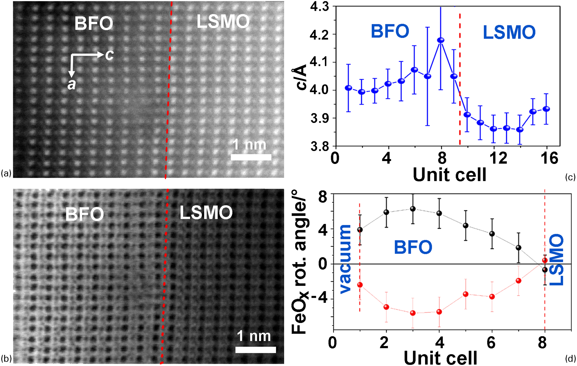
Lattice parameters and octahedral tilts in the vicinity of a BiFeO3/La0⋅7Sr0⋅3MnO3 interface determined from scanning transmission electron microscopy (STEM) images: a high-angle annular dark field (HAADF) STEM image of the interface; b bright-field (BF) STEM image of the interface acquired simultaneously with a; c graph of the c-parameter variation with position determined from the HAADF image; d graph of the octahedral tilt with position for the two sublattices determined from the BF image. From Pennycook and Varela, 167 reproduced with permission of Oxford University Press; based on the earlier Figs. 1 and 2 of Borisevich et al. 81
As for buried interfaces, line defects in materials are best probed by electron microscopy, and atomic-resolution microscopy is especially powerful when these line defects extend along a major crystallographic direction. Arredondo et al. 110 examined partial dislocations at Pb(Zr,Ti)O3/(La,Sr)MnO3 (LSMO) interfaces and the associated planar faults emanating from these partials into the LSMO using atomic-resolution HAADF imaging followed by quantitative processing to determine local strains around the dislocations and faults using the geometric phase algorithm. 111 In a similar manner, Lubk et al. have recently used the geometric phase algorithm to study dislocations and nanodomains in BiFeO3 thin films. 112
The Annular Bright Field (ABF) technique for light element imaging 56 discussed above has been well used by Klie et al. to examine oxygen ordering in Ca3Co4O9 and clearly shows buckling of metal–oxygen atomic planes in this structure 113 as had been hinted at in previous HAADF studies. 114 Similarly Zheng et al. have used a combination of ABF and HAADF imaging to elucidate the atomic structure of TiO2/LaAlO3 interfaces including the oxygen coordination. 115 The detailed oxygen bonding at MgO/Al2O3 epitaxial interfaces was revealed by ABF imaging in the recent publication by He et al. 116 It is to be expected that ABF imaging will be increasingly used in coming years for quantitative studies of oxide structures, in combination with the other techniques reviewed above.
It is of course the case that many of the same features can also be analysed using broad-beam conventional TEM, so it is worth saying a few words regarding the respective strengths of STEM and HRTEM techniques such as exit wave reconstruction or negative Cs imaging (NCSI), although there have been few direct comparative studies. Being a scanning technique, STEM is inherently more prone to noise, distortion and artefacts than broad-beam TEM, where an entire field-of-view can be imaged at once with rather short exposure times. As a result, AC-STEM was applied to quantitative picometre metrology of atomic structures somewhat after aberration-corrected HRTEM, which arguably lends itself more naturally to such high precision analysis. 73,99,100 As alluded to above, recent hardware and room environment improvements were instrumental in reducing the issues associated with scanning to a level compatible with picometre-precision imaging and, consequently, researchers using AC-STEM have benefitted from image analysis procedures already developed for HRTEM. It should be noted, however, that as with all advanced analysis techniques, great care must also be taken to avoid artefacts and distortions when using HRTEM for strain mapping or high precision imaging. 117 The availability of aberration correctors in HRTEM also led to exciting developments, in particular the so-called NCSI technique for which the optical parameters of the instrument can be adjusted very precisely to yield atomic-resolution images where all columns (heavy and light elements alike) are imaged with high contrast in a single image. 118 Unless using ABF (in which case simultaneous EELS acquisition is not possible anymore because of the detector geometry), multiple images are usually required to locate and identify all atoms with AC-STEM, even if simultaneously acquired. The correlation of features from two STEM images may therefore be needed in the analysis of both cation and oxygen positions in a complex oxide, whereas there is often no such difficulty in HRTEM NCSI. On the other hand, one of the most successful and powerful HRTEM techniques consists of using a series of images acquired at different defocus values to retrieve the phase and amplitude of the electron wave exiting the sample, which can then be directly correlated to the precise sample structure. 119,120 For exit wave reconstruction, the careful alignment and correlation of all the images in the focus series is again crucial and, as for STEM, instabilities may limit the ultimate precision achievable. Furthermore, the contrast reversals with thickness changes in HRTEM mean that samples need to be exceedingly thin (often just a few nanometre thick) and flat, which can make the preparation of artefact-free specimens very challenging. Because there are no such contrast reversals in HAADF imaging, it may be possible to use slightly thicker specimens, which are more likely to be representative of bulk structures, although for the most detailed analysis sample thickness requirements are just stringent. A downside of both techniques is that they are prone to suffer from artefacts if the sample is slightly tilted, if the illumination is slightly tilted, or if residual optical aberrations such as astigmatism affect the image, such things can happen locally on an oxide because of sample bending at the thin edge or localised charging. Thus, it should be clear from this very brief discussion that both aberration-corrected HRTEM and STEM will be extremely valuable to a deeper understanding of atomic structures of materials, provided great care is taken to record the highest quality of data possible and to minimise or account for any artefacts or non-idealities in the imaging. Nevertheless, this article focuses specifically on AC-STEM because of its ability to provide simultaneous imaging and spectroscopic information, which really sets it apart for the study of functional oxides.
Atomic resolved spectroscopy of functional oxides
Early work on aberration-corrected STEMs using electron energy-loss spectroscopy mainly benefitted from having smaller probes to collect spectral data from smaller areas of about atomic dimensions and from having sufficient current in such small probes to be able to collect meaningful data from such small areas. Examples of this include the work of Varela et al. 117 and Klie et al. 118 on interfaces involving YBCO high T C superconductors.
A particularly impressive achievement that has been enabled by the development of atomic-resolution EELS has been the study of single substitutional atoms in oxide crystals. This was first demonstrated by Varela et al. in 2004 119 showing that heavy La ions could be not only imaged using the HAADF mode but also proved to be La using EEL spectroscopy. More recently, Rossell et al. 120 have shown that using a combination of imaging and spectroscopy that Ba dopants in SrTiO3 are not randomly distributed but tend to cluster, which possibly induces the formation of polar nanoregions in the SrTiO3 crystals.
The step change in the application and indeed the usefulness of EELS has come since the introduction of truly atomic-resolution spectrum imaging, where the probe is scanned across a defined pattern, along a one-dimensional (1D) line or 2D area, and spectra are collected from every point on the scan. 121 This makes extra demands on the instrument, as compared to imaging alone, since imaging is generally performed with pixel dwell times of just a few tens of microseconds per pixel, whereas aquiring good quality EELS data require much longer acquisition times (originally hundreds of milliseconds, although newer instruments and spectrometers will produce good quality data at shorter times down to 10 ms or less per pixel). As a result it is much slower to acquire a spectrum image than to acquire an HAADF image by a factor of 1000 or more, which has a number of effects. First, the microscope environment must be extraordinarily stable, including suppression of vibration, background noise, air-pressure variations (e.g. from air conditioning systems), air temperature and cooling water temperature stability, and stable background magnetic fields (or screening/compensation of instabilities). Moreover, the microscope and spectrometer must also be extraordinarily stable including the specimen stage, the high tension supply, the lens power supplies, and critically for AC-STEM, the corrector electrical supplies. If this stability is not achieved, then jitter or drift will tend to wash out all the atomic-resolution detail in the spectra. Nevertheless, because of the time required for acquisition, robust drift correction procedures are often required in the acquisition control system. Moreover, many oxide materials are insulators and may charge under the beam, requiring limited doses or rather quick (if noisy) acquisition to minimise charging. Furthermore, some materials are beam sensitive and either direct radiation damage or indirect damage via heating may destroy the very object that is under study, thus limiting the possible acquisition time per pixel. Either of these latter two effects therefore requires fast acquisition and may result in rather noisy spectra. Finally, any free organic contamination on the sample, the sample holder or the microscope vacuum can be broken down under the intense electron beam resulting in carbon deposition on the sample surface and an increased background in spectra, requiring very clean samples and holders. All these limitations have meant that much better spectrum imaging has been possible with more recent STEM instruments equipped with more recent EEL spectrometers and although imaging studies with AC-STEM started in the early 2000s, atomic-resolution spectrum imaging studies have mainly been appearing in print since 2007.
The earliest demonstrations of the power of atomic-resolution spectrum imaging to study the atomic chemistry of oxides were provided by studies of manganese containing oxides such as Bi0⋅5Sr0⋅5MnO3, 122 La1⋅2Sr1⋅8Mn2O7, 123 and (La,Sr)MnO3/SrTiO3 multilayers. 124 For example, Fig. 6 shows the atomic-resolution mapping of La, Ti and Mn in (La,Sr)MnO3/SrTiO3 multilayers along a <001> direction of the primitive perovskite. 128 These compounds have the advantage of containing elements with convenient edges for EELS such as the Mn L2,3 edge at 640 eV, which is marked by a sharp onset and two ‘white lines’, and the La M4,5 edge at 832 eV, which also has a very sharp onset with two extremely intense ‘white lines’. Additionally, both Bosman et al. 122 and Kimoto et al. 123 showed that it was possible to map oxygen in these materials with atomic resolution. In the case of Bosman et al., 122 oxygen was mapped in both the [100] and [110] projections, and the expected buckling of the oxygen planes because of octahedral tilting was observed in the latter, corresponding to the BF imaging studies mentioned above. 80,81 Further studies of note since these initial reports include work on (La,Sr)MnO3/SrTiO3 multilayers, 125 LaVO3/SrTiO3 multilayers, 126 Bi2(Fe1/2Cr3/2)O6, 127 SrTiO3/BaTiO3 interfaces, 128 and defects in LaNiO3/LaAlO3 superlattices. 129
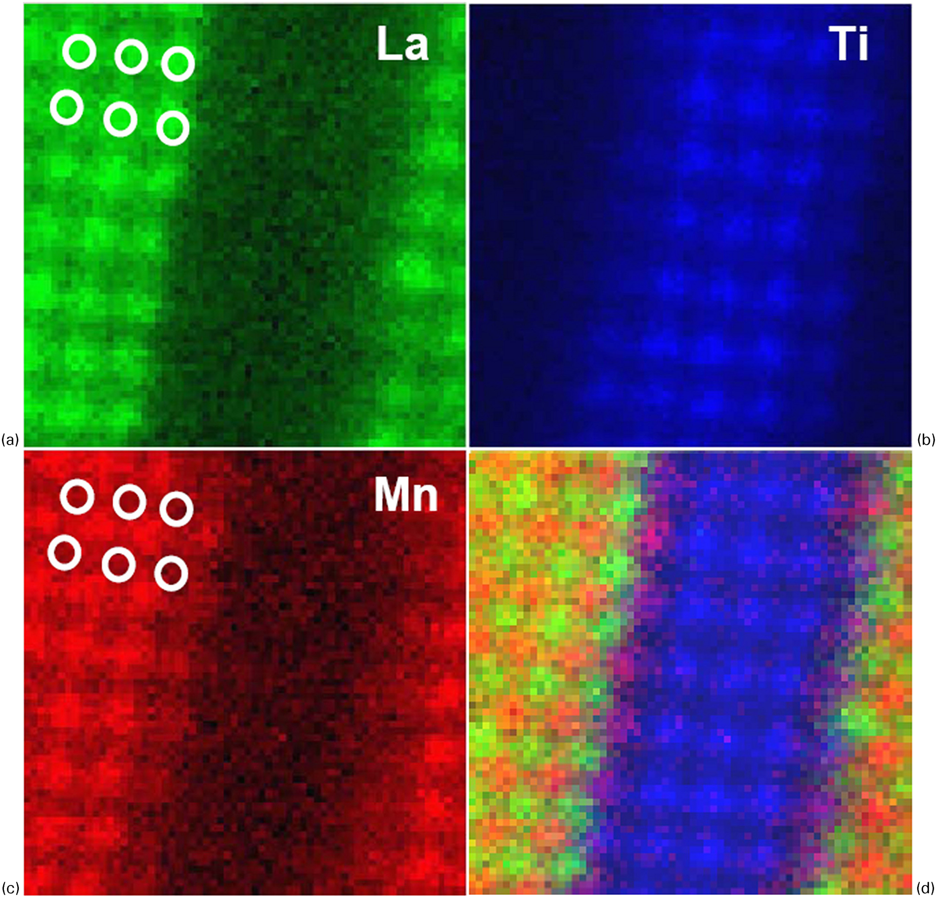
Electron energy-loss spectroscopy (EELS)-SI spectrum imaging mapping of a La0⋅7Sr0⋅3MnO3/SrTiO3 multilayer showing a La M4,5 map; b Ti L2,3 map; c Mn L2,3 map; d three-colour composite map of Mn (red), La (green), and Ti (blue). From Muller et al. 124 Reprinted with permission from AAAS
Another possibility with EELS is not just to quantify what elements are present in an oxide, but how they are bonded to each other or to detect oxidation state changes, since such things cause significant changes to the shape of EELS edges (a field of study that is generally referred to as energy loss near edge structure: ELNES). Muller et al. 124 showed in 2008 that it was possible to image chemical bonding changes at the interfaces in a La0⋅7Sr0⋅3MnO3/SrTiO3 multilayer with atomic resolution using the fine structure at the Ti and Mn edges. This possibility to image not only atomic-scale chemical composition but also atomic bonding was also taken advantage of by Varela et al. 130 to image oxidation states in lanthanum manganites. In a similar manner, the oxidation state of Mn at interfaces between La2/3Ca1/3MnO3 and a SrTiO3 capping layer was studied by Estradé et al. 131 showing that Mn is reduced close to the interface for [001] grown layers, whereas no such effect occurs for [110] layers. Similar atomic-resolution studies of oxidation states have been performed by Tan et al. 132 on Mn oxidation state variations within the unit cell of Mn3O4 and by Turner et al. 133 on the reduction of CeO2 at surfaces of nanoparticles.
Ever since the surprising discovery of metallic conductivity at the interface of two band insulators, SrTiO3 and LaAlO3, by Ohtomo and Hwang, 2 there has been a large number of studies and a lively debate about the origins of this effect in SrTiO3/LaAlO3 and other oxide heterointerfaces, and a number of models have been proposed. Aberration-corrected STEM has played an important role in understanding this. Detailed atomic resolved EELS studies were performed by Shah et al. of LaMnO3/SrTiO3 and LaMnO3/SrMnO3 superlattices, and these showed very clear electronic reconstructions at the interfaces in such superlattices with charge transfer from the bulk to the interface. 5,6 Initial studies of the SrTiO3/LaAlO3 interface found that in some interfaces with the layer sequence AlO2/LaO/TiO2, there seems to be charge transfer and excess electrons at this interface. 134 Reduction in Ti valence at such interfaces coupled with a polarisation of the surrounding cells has also been seen by Cantoni et al. 11 On the other hand, other studies of SrTiO3/LaAlO3 using atomic-resolution STEM EELS seem to suggest no significant charge transfer or valence variation in this interface and instead suggested interfacial intermixing and lattice distortion as partly responsible for the effect. 135,136 A recent careful study of this interface grown under a range of conditions including quantitative atomic-resolution EELS also clearly shows that the conducting interface formation is triggered by slight Al excess in the LaAlO3 and that this Al dopes onto the La sites causing a diverging potential and a resulting charge accumulation at the boundary. 137 While no final conclusions can yet be reached on the origins of the 2D electron gas (2DEG) in all such interfaces, it is clear that details of deposition conditions resulting in slight deviations from stoichiometry or layer mixing play a key part, and the atomically resolved analytical capabilities of aberration-corrected STEM will be key to unravelling this.
Other studies of note using ELNES mapping include those by Klie et al. on O bonding in Ca3Co4O9, 113,114 MacLaren et al. on O bonding in Nd-nanorod precipitates in doped BiFeO3, 99 and those of Haruta et al. 138 and Mundy et al. 139 where the hybridisation of O 2p with atomic orbitals around the different metal atoms is mapped in two different mixed oxides, La2CuSnO6 and LuFe2O4. Another thing that can be mapped using careful atomic-resolution ELNES is the O coordination of atoms, even without any change in oxidation state and this has been demonstrated for Ca2FeCoO5 brownmillerite, 140 Pb2Sr2Bi2Fe6O16 141 and Sr4Fe6O12+δ . 142
Combining techniques: imaging, spectroscopy, and theory
In the past, there has been a tendency to either concentrate on imaging-based studies or spectroscopic studies in the electron microscope. These were sometimes combined in the form of a detailed imaging study, with spectroscopy being recorded at key features such as an interface or a defect and compared with spectra away from the feature in the bulk. The advent of spectrum imaging has now allowed explicit correlation of image features to chemical identity, even in complex multicomponent systems. A good early example of this is provided by the study of Arredondo et al. 143 where the atomic structure of misfit dislocations at Pb(Zr,Ti)O3/SrTiO3 interfaces is investigated and the local strain is revealed using geometric phase analysis and correlated with spectroscopy data. EDX spectrum imaging reveals significant Pb segregation to the highly strained region around the dislocation core and EEL spectra show that the electronic structure is strongly modified in this core; this correlates well with theoretical predictions.
Going beyond this, combining the kind of quantitative imaging of atomic structures outlined above with atomic-resolution spectrum imaging now means that atomic models can now be constructed from image data with a precision in atom location of may be 10 pm, or even better. The identity of each atom in the model can then be identified using spectrum imaging, allowing 2D models of the atomic-scale chemical structure of complex features to be built up. Additionally, if an object is such that it can be imaged with atomic resolution from two or more projections, then it may be possible to reconstruct its three-dimensional atomic structure via a discrete tomography approach. 144 This kind of approach can then be applied to complex oxides to allow atomic-resolution reconstruction of the three-dimensional chemical structure. This has been recently done by the present authors together with co-workers for novel Ti-rich anti-phase boundaries in Nd/Ti-codoped bismuth ferrite, as illustrated in Fig. 7. It was possible from HAADF/BF image pairs recorded simultaneously from two orthogonal projections of the same type of planar boundary to work out the three-dimensional coordinates of every atom in the boundary and surrounding region (including the oxygen atoms). The three-dimensional chemistry was reconstructed from the EELS spectrum images showing the Ti and Fe distributions, in particular. The resulting model showed excess negative charge in the boundary resulting in strong polarisation of the first few unit cells to either side of the boundary and the stabilisation of a locally polar phase at the expense of the bulk anti-ferroelectric phase, and thus established that pseudotetragonal polar-ordered phases in BiFeO3 may be stabilised by electric field alone without large substrate constraint.
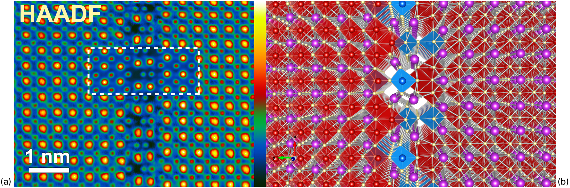
A three-dimensional model of an anti-phase boundary in Ti- and Nd-doped BiFeO3 constructed from atomic-resolution high-angle annular dark field (HAADF) and bright-field (BF) images together with atomic-resolution chemical maps from two orthogonal projections: a HAADF image from the first projection. An inset (delimited by a dotted white box) shows an image simulation of the model in b carried out using the multi-slice algorithm as implemented in the QSTEM software suite; 148 b atomic model prepared using VESTA 168 (Fe: red, Ti: blue, O: yellow, Bi: purple). After MacLaren et al., 106 used in accordance with the Creative Commons Attribution 3·0 Unsupported License
Another possibility afforded by the atomic-resolution quantitative characterisation enabled by aberration-corrected STEM is the chance to combine these experiments with theory and simulation, both in terms of testing and validating theoretical models, as well as in developing sophisticated models of atomic-scale behaviour beyond the limits of either experimental analysis alone or theoretical prediction alone. There are two main classes of theoretical approach that can be used well in combination with this atomic-resolution characterisation: phenomenological semi-classical continuum models and ab initio quantum mechanical models. These will be discussed in turn.
Phenomenological models of behaviour tend to work in terms of bulk properties or parameters that describe a collective property of a material. Nevertheless, and perhaps surprisingly, they often still provide a useful insight into the atomic-scale behaviour of materials. For example, treatment of continuum electrostatics using approaches like the Landau–Ginzburg–Devonshire equation has proved powerful in understanding behaviour at interfaces in functional oxides such as in the study of BiFeO3/La x Sr1−x MnO3 interfaces by Chang. 83 Similarly, phase field modelling has been used in understanding the atomic structures of La0⋅5Sr0⋅5CoO2⋅5 films grown on NdGaO3 as revealed by HAADF-STEM. 85
The obvious alternative to classical continuum models is to explicitly consider the quantum mechanics through the use of density functional theory (DFT) simulations. Codes for this purpose such as CASTEP or VASP are now readily available, and the computer power to run realistic simulations of many oxide superstructures is now available in many facilities worldwide. Because DFT explicitly considers the valence and conduction electrons in a periodic supercell, it provides insights not only into the minimum energy structure, or the energies of alternative structures, but also into the electronic structure. Thus, studies combining atomic-resolution microscopy and DFT simulation may concentrate on either structural aspects or electronic structure, or indeed highlight both. For example, the initial report of a supertetragonal phase in compressively strained BiFeO3 films was coupled with DFT simulations of the variation of the cell with strain, which showed clear stabilisation of such phases at compressive strains of >4⋅5%. 17 A very recent example of this class of work is the study by Kim et al., 16 which combined quantitative processing of STEM imaging showing the suppression of ferroelectricity in BiFeO3 films through tilt suppression in the proximity of an interface with DFT simulations explaining the electronic origins of the effect at the atomic level.
There are several nice examples of the combination of aberration-corrected microscopy with theory to understand the electronic structures of specific nanoscale features. For example, Wang et al. combined structural studies of LaAlO3/TiO2 interfaces using HAADF imaging with studies of the electronic structure of the interfaces in order to explain the semiconductor–metal transformation at the interface. 145 Similarly, Borisevich et al. used a combination of quantitative evaluation of AC-STEM images and DFT calculations to probe the correlated structural and electronic structure changes at BiFeO3–La0·7Sr0⋅3MnO3 interfaces. 81 More recently, Bocher et al. used STEM imaging and EELS combined with DFT simulations to understand the atomic, electronic and magnetic structure of ferroelectric–ferromagnetic interfaces in artificial multiferroic tunnel junctions. 146 Pennycook and coworkers showed using a combination of atomic-resolution imaging, experimental EELS and DFT simulation of structure and EEL spectra, that thin films of yttrium-stabilised zirconia sandwiched by SrTiO3 have a highly disordered oxygen sublattice, which may well explain the reports of ultra-high oxygen ion conductivity in these heterostructures. 147,148 A particularly insightful combination of atomic-resolution imaging, EEL spectroscopy from several sample thicknesses and DFT calculation was used to determine the details of a c(4×2) surface reconstruction of a SrTiO3 crystal. 149
In magnetically ordered materials, the spins on the atoms will be ordered in regular patterns, and this will have an influence on the fine structure of the EELS edges. This fact has recently been used by the combined EELS and DFT study of Gazquez et al. 150 to show that Co2+ ions in strained La0⋅5Sr0⋅5CoO3−∂ order spontaneously into atomic stripes of low- and high-spin states in a similar manner to the earlier experimental study of Yang et al. on Ca3Co4O9. 151 This was done by careful analysis of the EEL spectra from different layers in the crystal structure and comparison to DFT calculations. Salafranca et al. took this one step further and translated the electron energy-loss magnetic circular dichroism technique of Schattschneider et al. 152 into a real space mapping technique to study the magnetisation of Fe3O4 nanoparticles at a resolution of a few ångströms and to show that the magnetisation at the surfaces could be influenced by organic surface layers. 153 As with the work of Gazquez et al., 150 DFT was used to explain the atomic-scale mechanisms underlying the experimental observations.
Clearly, there may be cases where combining quantitative structural measurements, atomic-resolution spectroscopy, and DFT simulations will yield great benefits. This was recently achieved by MacLaren et al. 99 who determined the three-dimensional atomic structure of a novel NdO x nanorod precipitate in Nd, Ti-codoped BiFeO3; this is summarised in Fig. 8. Additionally, the DFT calculations revealed that the electronic structure in the vicinity of the defect is strongly modified with a much reduced bandgap, indicating that the nanorods would function as novel 1D semiconducting channels in insulating BiFeO3.
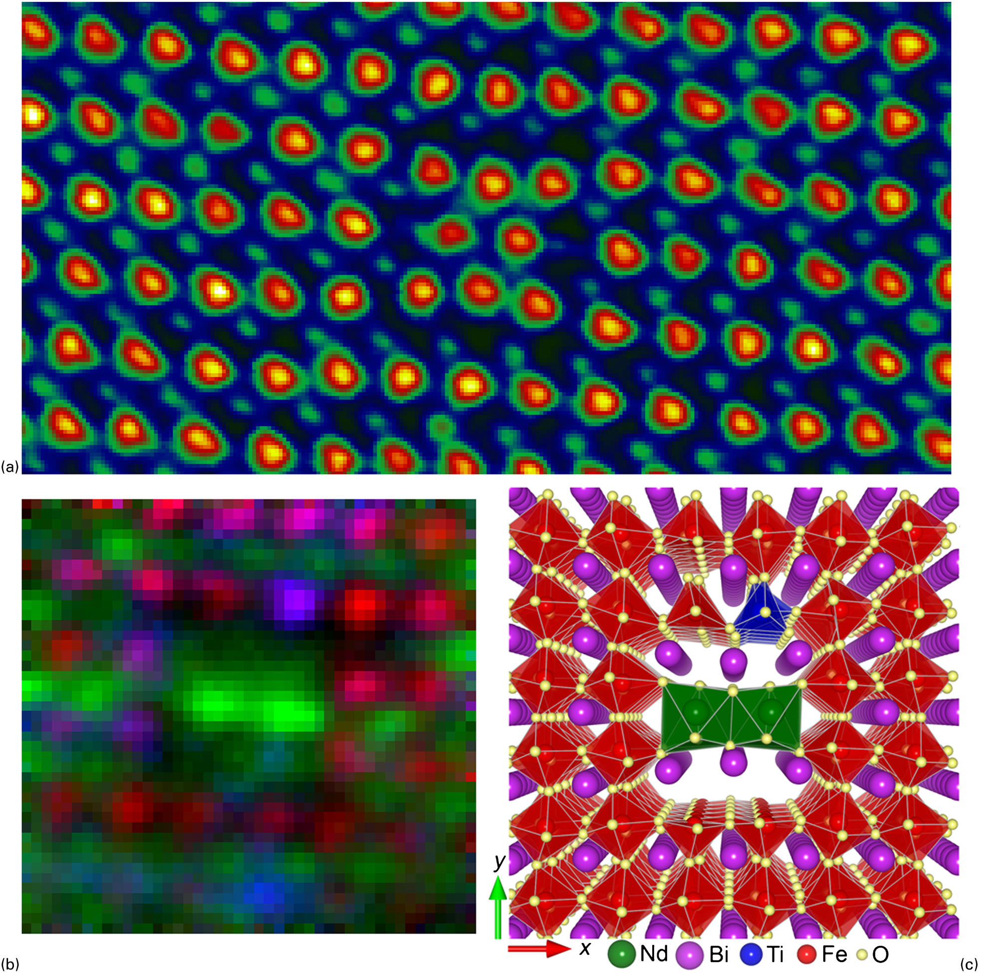
Combined atomic-resolution imaging, spectroscopy and density functional theory (DFT) reconstruction of a two-atom wide nanorod precipitate in Nd, Ti-codoped BiFeO3: a high-angle annular dark field (HAADF) image of one such precipitate in the end-on direction (that is, observed down the [001] direction of the perovskite lattice); b coloured elemental map of the precipitate (Fe: red, Nd: green, Ti: blue), revealing how Nd-rich columns form the core of the precipitate while its periphery is enriched in Ti. This and elemental maps (and images) of equivalent precipitates observed along the perpendicular [100] direction are used to create an initial three-dimensional model of the precipitate structure; c final DFT-refined model structure (Fe: red, Nd: green, Ti: blue, O: yellow, Bi: purple) represented using VESTA. 149 Based on data presented in MacLaren et al. 99
Future directions in aberration-corrected STEM of functional oxides
The existing instrumentation and techniques outlined above have already allowed great strides towards a better understanding of functional oxides at the atomic scale, whether as bulk materials, thin films or heterostructures. It is of course anticipated that increasing use will be made of such possibilities, in combination with complementary techniques including X-ray diffraction, X-ray photoelectron spectroscopy (XPS), scanned probe microscopies, and other localised or bulk property measurements. Nevertheless, there are other advances in instrumentation currently arriving that will enable further huge strides in our ability to characterise materials and nanostructures at the atomic scale, and thus subsequently impact greatly on the atomic design of functional oxides.
First, there is the development of dual-range or multiple-range EELS. Conventionally, if the microscope was set up to give a bright enough beam and the spectrometer set up with appropriate acquisition parameters for the area of interest in the EEL spectrum (e.g. at several hundred electronvolts of energy loss), then these conditions would be totally unsuitable for the recording of low-energy-loss data including the bright zero-loss peak. On the other hand, under conditions suitable for recording low loss data, the higher energy-loss data would be too noisy for serious use. A new approach was developed at Glasgow, whereby the high loss data could be collected under appropriate conditions, immediately followed by the low loss data with very short acquisition times enabled by fast (microsecond) shuttering with an electrostatic deflector. 154 This has since been commercialised by Gatan Inc. and has been integrated into the latest generation of EEL spectrometers that are now being installed onto the latest electron microscopes. There are several advantages to such dual-range spectrometers: of particular interest for the quantitative study of functional oxides is the ability to deconvolve multiple scattering out of the core loss EELS data using simultaneously acquired low loss data. This enables a better quantification of the spectroscopy, whether for stoichiometry or ELNES and it may, for example, allow direct counting of atoms in each atomic column across a feature of interest in an oxide nanostructure (at least in such cases where the sample is thin enough so that beam dechannelling is insignificant). The application of such atomic-resolution dual-range EELS will open up a new era of fully quantitative atomic-resolution chemistry.
Second, monochromated STEMs are now being delivered that promise to combine atomic resolution with energy resolutions down to better than 30 meV. 155 This is better than an order of magnitude improvement on the energy resolution available in the conventional CFEG instruments (about 0·35 eV) and allows us to dream of major new possibilities. This would allow the resolution of bandgaps in even narrow bandgap semiconductors, and would therefore allow the explicit mapping of electronic structure around defects and interfaces in functional materials, including the functional oxides that are the principal topic of the present review. Furthermore, such high energy resolution may start to allow the resolution of very small energy excitations associated with lattice vibrations and thus the possibility of studying phonon behaviour at the nanoscale.
Third, recent work has suggested the use of novel imaging detectors for particular applications in aberration-corrected microscopy. For example, Shibata et al. 156 used a segmented detector to record differential phase contrast from a ferroelectric at atomic resolution. In a different connection, Huang et al. 157 tuned the angular range detected on their ADF detector to highlight diffraction contrast arising from high-order Laue zones and thereby obtain information from the projection direction into their images, thus providing some degree of three-dimensional characterisation from a 2D STEM image. Recently, Kimoto and Ishizuka demonstrated atomic-resolution diffractometry, and this could be used to reveal additional information at the atomic scale. 158 It is to be expected that further novel use of imaging detectors to explicitly use diffraction or phase contrast in the formation of STEM images will become an increasing feature of future atomic-resolution studies of functional oxides.
The use of multiple signals simultaneously acquired is likely to be an increasing feature of aberration-corrected STEM on oxides. This may include the combination of EELS, X-ray spectroscopy, 68 cathodoluminescence, 159,160 and secondary electrons 167 in order to provide a complete quantitative picture of the structure, chemistry and properties at the atomic or nanoscale.
Finally, in situ studies of processes at the atomic scale and not just static structures are likely to become increasingly important as capabilities for in situ experimentation inside corrected microscopes are developed. Many of these techniques have not yet been applied to functional oxides, but this can be expected as the techniques become more widely available or at least widely known in the scientific community. This may include studies of changes in response to temperature, 162 gas phase 163 or liquid phase chemical reactions 164 in specially constructed cells, response to mechanical stress, 165 and electrical stimuli. 105,166
Conclusions
It has been shown that aberration-corrected STEM has revolutionised our understanding of functional materials in the past few years. This has included unprecedented picometre metrology of atomic structures in two and three dimensions; atomic-resolution spectroscopy revealing variations from one atom to the next in composition, local bonding, electronic structure, and even magnetic ordering; and detailed correlations with theory and atomistic simulations. Undoubtedly, this has also been stimulated by advances in computational and simulation techniques, as well as developments in thin film growth techniques that are now allowing sub-monolayer control of heterostructure fabrication. Nevertheless, it is clear that these advances in microscopy have arrived at just the right time to provide the understanding that is necessary for the atom-by-atom design and fabrication of next-generation materials, heterostructures and devices. As such, it is clear that the future development of materials will be critically dependent on the application and further development of aberration-corrected STEM.
Footnotes
Acknowledgement
IM is thankful to the EPSRC for funding of the SuperSTEM facility over many years, as well as for the provision of specific research grants that funded some of the work featured in this review (grant reference numbers: EP/H028218/1, EP/I000879/1, EP/J009679/1) and the provision of a PhD studentship to Dr LiQiu Wang.