
Abstract
Printed circuit boards (PCBs) have a sandwich structure consisting of an insulating composite layer between conductive copper layers. The material property of the PCB cannot be defined as isotropic due to this special structure. In addition, variables such as the types of hundreds of components on the PCB, material properties, types of solder leads, and thickness of the sandwich structure make it very difficult to create and verify the finite element model of the PCB. The aim of this study is to perform a sensitivity analysis by defining the strain values measured from three points on the PCB with the help of strain gauges as responses and to find the best design variables that correlate with the physical test. The effect of each design parameter on the response function was examined, and the results were obtained with statistical data. The objective function and constraints were determined to find the best correlated finite element model with a physical test, and the best design was obtained by running the optimization model. In this way, the finite element model was calibrated by taking into account the thermal stresses resulting from the heat generated by the transistors and by using optimization methods.
Keywords
Introduction
A printed circuit board, commonly referred as PCB, is a mechanical component that binds electronic components together and electrically connects them. Printed circuit boards have many sandwich-like layers, and the construction materials of these layers are also different from each other. The variability of this sandwich structure makes it very difficult to create and verify the finite element model (FEM) of the circuit board. 1 In the literature, it is possible to find many studies on obtaining the best circuit board model by using experimental design, and optimization methods.
In real-world applications of computer-aided engineering-based optimizations in the virtual prototyping process, it is not always possible to reduce the complexity of physical models and obtain numerical models that can be solved quickly. Typically, each numerical simulation takes hours or even days. 2 As a result, efficient meta-models have become alternatives to costly design studies. In addition to providing an automated approach to the selection of the most appropriate metamodel for the problem, an independent test dataset should be used to evaluate the prognostic quality of the metamodel. Therefore, the selected metamodel with the best prognosis quality is called the meta-model of optimized prognosis (MoP). By using advanced filtering techniques, an efficient approach is also provided for high-dimensional problems with the automatic reduction of the variable space. 3
In the literature one can find many different studies about analyses which were made using the experimental design methods to examine the reliability of PCBs under different environmental conditions. Fang et al. 4 analyzed the temperature deviation between test and simulation and determined the main influencing parameters by sensitivity analysis. Finite element software was used to obtain the modal frequencies of a PCB, and the first six modes were extracted. Gao 5 defined the coordinates of the boundary condition points of the PCB as the design parameters and the modal frequencies as the response function and established the optimization model. A model with the most suitable connection center coordinates was obtained. Xu et al. 6 performed modal and fatigue analysis to obtain the most suitable PCB model and determined the design variables (material properties of the anisotropic PCB) and response functions (solders between the component and the PCB). In the study, the most suitable PCB material was obtained for the safety of solders in critical areas. Han et al. 7 performed vibration and PSD analyses of the PCB and solved the model at different component positions. For each component position on the PCB, an FEM was compared, and the best one was found by using optimization tools. Xia et al. 8 defined some design variable parameters, such as material properties, thickness of the board and terminals, and expansion coefficients, and obtained contributions from these parameters by using the experimental design method to improve the thermal fatigue resistance. Maia Filho et al. 1 carried out experimental designs with three different component positions for the purpose of mechanical property characterization of the PCB. He obtained strain values on the PCB by using strain gauges and created an optimization model to find the best design. Chaudhari et al. 9 examined the mechanical behavior of the PCB at high temperature changes by creating an FEM and solving thermal mechanical analysis. Serebreni et al. 10 studied the effect of boundary conditions on a PCB, created a thermo-mechanical finite element analysis (FEA) model with electronic components, and obtained the strain values on the circuit board. Most et al. 3 performed sensitivity and optimization studies. The Adaptive Metamodel of Optimal Prognosis (AMOP) method was used for the sensitivity analysis and advanced Latin Hypercube Sampling methods for the optimization process. Hungtingron et al. 11 developed the AMOP from the idea of deleting insignificant input variables from the model. As a result, the forecasting quality of the approximation model has improved. Through the use of advanced filtering techniques, automatic elimination of variables has been achieved. An efficient optimization was also enabled for high-dimensional problems. Salahouelhadj 12 created an FEM with anisotropic materials to investigate the effects of the parameters on the behavior of the circuit board, such as plate thickness, diameter of vias, and thickness of the PCB. McLeish et al. 2 carried out a study on the use of Sherlock software in the creation of the PCB model. Hu et al. 13 studied the conductive copper layer of the PCBs and investigated the structural effects of the copper mask on the circuit board. Nowak et al. 14 examined the thermo-mechanical properties of the PCB, carried out various loading scenarios, and compared the results with the physical test results. Kalyani et.al. 15 examined the material characteristics of the PCBs and carried out modal analysis of the circuit boards with two isotropic and anisotropic materials. Arabi et al. 16 created an FEM of the PCB and performed modal vibration analysis; as a result, the effects of the material type used in the circuit board were obtained. Gharaibeh et al. 17 investigated the effects of anisotropic material properties on the PCB and its components and correlated them with the physical test by creating an FEA model including both free and fixed boundary conditions. Wei et.al. 18 examined the effects of the boundary conditions of the PCB in the FEM and found three designs with different boundary conditions that made the analysis results effective.
The aim of this study is to perform a sensitivity analysis by defining the strain values measured from three points on the circuit board as responses and to find the best design variables that correlate with the physical test.
Figure 1(a) shows the components used in automotive lighting. The LED driver used in the rear lamp is shown in Figure 1(b). The PCB layers are formed by sandwiching the insulating FR-4 material between copper layers with conductive paths on the surface, and these pathways provide the conductivity on this surface. In addition, it is covered with a solder mask in order to protect the copper layer from external factors such as dust, corrosion, and oxidation. The sandwich structure of a circuit board consisting of conductive and insulating layers is shown in Figure 1(c). (a) Internal structure of rear lamp, (b) printed circuit board, (c) PCB layers.
Material and methods
Firstly, the circuit board layout, which includes different types of components, position information, and materials of the circuit board, has been imported to the Ansys Sherlock 2022 R1. By importing the circuit board, the materials of all the components in the circuit board are synchronized with the local library. The thermal map processing and importing feature of Sherlock was used in order to take into account the pre-stresses that LEDs create on the circuit board under operating condition. This method is used frequently in automotive lighting development processes. The components on the PCB, core layer, and leads of electronic components were created automatically in Sherlock and exported to Ansys Workbench 2022 R1. Strain values were read from three different points with the help of strain gauges while the LED was running, and the strain results were evaluated to validate the FEM. The experimental model was established by defining strain values obtained from physical tests as the response functions, the modulus of elasticity, the thermal expansion coefficient of the solder mask, and the boundary condition of the PCB as the design parameters.
The effect PCB optimization workflow.
Thermal structural analysis
Numerical modeling and boundary conditions
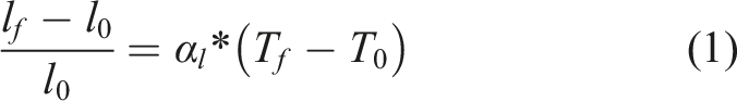
Most solid materials tend to expand when heated and contract when cooled. The expression for the change in length with respect to temperature for a solid material is as follows:


Boundary conditions and materials used in the numerical simulation.

Thermal map measurement
During the operating conditions of the LED component on the PCBs used in the automotive lighting industry, heat generation results in pre-stress on the board. For this reason, it is very important to consider this situation when creating the finite element calculations for PCBs.
The FLIR SC 620 thermal camera was used to measure the temperature on the surface of the PCB under the LED operating condition. The PCB was connected to a 13.5 V power supply, and the LED light was powered and held for 30 min until the temperature distribution to reach steady state. Then, the measurement was made using a thermal camera.
Using the system in Figure 3, the temperature on the surface of the PCB was measured, and the temperature distribution was obtained as shown in Figure 4. Thermal camera measurement system. Thermal camera map image of PCB.

It is very important that the image collected from the circuit board by the thermal camera to be verified by FEM. FloEFD software was used for this purpose. FloEFD is fully CAD-embedded CFD software, and it is possible to analyze external and internal fluid flows, steady-state and time-dependent fluid flows, and heat transfer in fluid, solid, and porous media. It also includes the LED module, battery module, and FLOEDA Bridge that can help to simulate thermal distribution on PCBs. The EDA Bridge module provides capabilities for the detailed import of PCBs. Radiative surface and components in the layers of the PCB were defined by using this software, which is used for PCB analysis as a module on FloEFD. It was considered that the PCB powered by 13.5 V and 0.18 amps. Therefore, the powers of transistors were calculated at 0.486 W and defined in EDA Import. The Monte Carlo method was used with an environmental temperature of 22°C.
Experimental setup and strain gauge positions
A schematic view of the experimental setup for PCB strain measurement is given in Figure 5. The components of the test setup were (1) a PCB, (2) strain gauges, (3) a data logger, and (4) a computer. Strain gauge positions on the PCB are demonstrated in Figure 6. Three strain gauges were attached to the regions where the maximum strain occurred in the FEA. The test was performed for 30 minutes under the LED’s operating conditions. Test setup. Location of strain gauges on PCB.

In the test setup, thermal camera, data logger, strain gauge, and power supply were used. European origin FLIR SC620 thermal camera was used to take thermal measurements on the PCB. The main features of the thermal camera are the following: −40°C to +500°C temperature range, 40 mK thermal sensitivity at 30°C, 640 × 480 pixel infrared resolution, and 24° × 18° 0.3 m field of view. Japanese-origin Graphtec midiLogger GL840 data logger was used to measure, process, and compile thermal temperatures and strains on the PCB. The main features of the data logger are as follows: ±0.1% FS voltage measurement accuracy, 14 bits resolution, 1 MΩ input resistance, and 20 analog input channels. Germany-origin HBM 3/350RY88 type strain gauges were used to measure the strain values on the PCB during the test. The main features of the strain gauges are as follows: 350 Ω ±0.3% resistance, 101 ±10 10−6/°C temperature coefficient of gauge factor, 2.08 ±1% gauge factor, and 0.2% transverse sensitivity. China-origin Manson HCS-3302 type power supply was used to power the LED on the PCB. The main features of the thermal camera are the following: 220–240 V input, 1–32 VDC output, 50/60 Hz frequency, and 2.4 A max amperage.
Printed circuit board FEM model
Utilization of Sherlock software for printed circuit boards
Sherlock is software that performs static and dynamic finite element analyses for electronic circuit boards. In addition, reliability and strength analyses of electronic circuit boards can be performed. This module is used for structural analysis of electronic circuit boards in automotive, aerospace, and many other fields. Electronic circuit boards include various components, such as transistors, resistors, capacitors, lighting elements, diodes, and integrated circuits. Factors such as the large number of components on the PCB, the different materials of each component, and the scattered locations make modeling with classical finite element software very difficult. Sherlock module makes the work much easier and saves time by including different types of components and a wide range of materials for electronic board design. 2
Some steps followed to create the FEM of the PCB in Sherlock software are shown in Figure 7. FEM Model creation workflow for PCB.
Printed circuit board FEM model setup
Based on the flow chart of Figure 7, by importing the circuit board layout, the materials of all components were synchronized with the local library. The loading conditions of the circuit board under the operating conditions (LED open status) are defined, and the life cycle is created. Along with the thermal map processing feature, which is frequently used in automobile lighting, the pre-stresses that the LED creates on the circuit board under operating condition are also included in the model. The automatic creation of the detailed element structure increases the precision of the result
Importing the PCB layout to Sherlock, which includes specific features of the PCB, is a very efficient method, especially for saving time. Importing the PCB layout as shown in Figure 8 includes the following: component type Importing PCB into Sherlock.
Components on the PCB layout require updates from the local component library or from the extensive component library of Sherlock software. In this study, a library update was performed to select the proper sizes, material properties, and connection types of components.
The duration and the frequency of the environmental loads on the PCB were defined. A loading profile was created between the room temperature and the LED operating condition, as shown in Figure 4.
It is important to include the thermo-mechanical stresses on the PCB caused by the temperature difference. The temperature distribution of the PCB measured by a thermal camera has been processed in the Sherlock module. The processed thermal image was imported into the model and used as a loading condition for the analysis. Exporting process between Sherlock and mechanical. Sensitivity and optimization workflow.

A PCB FEM model with 3D elements was created automatically in the Sherlock module. The PCB core, trace (conductive layer on the PCB), mount points, drilled holes, and components placed on PCB leads (pin that connects component and PCB) were modeled in detail. A bonded mesh type with a 0.5 mm first-order element size was used for PCB core, components, and leads modeling.
PCB model that was created in the Sherlock module was exported to Ansys Workbench. Mesh structure, mesh type, material properties of each component, lead type, and drilled holes were also exported (Figure 9). The export parameters of Sherlock to Ansys Mechanical are listed below: • Mesh type: Bonded. The Bonded type makes contacts between components within a tolerance of 0.1 mm. The Bonded model type uses a method in which the PCB and all components are meshed individually. Such individual meshing typically yields more uniform 3D elements for both the PCB and all components. After all 3D elements are created, Sherlock then automatically “glues” the components to the PCB by creating constraint equations between each component element and the corresponding PCB element(s). Uniform 3D elements can improve the accuracy of results, but the constraints required to define the additional bonds typically increase the analysis time. The bonded method also allows more complicated models to be created.
20
• PCB Model: Layered. The Layered Elements Model creates elements like the Layered Model that only span a given PCB layer, but it assigns individual material properties to each element based on the percentage of materials covered by the element itself. This model generates the most PCB elements and the most localized material properties of any Sherlock-provided PCB model. The elements defined for each layer share nodes with the elements in the layers above and below, eliminating the need for surface ties in the FEA model.
21
• Element order: First order. The Element Order property indicates the type of FEA element to be used to model the PCB. First-order elements (i.e., 8-node bricks and 6-node wedges) result in reduced analysis time but stiffer elements. Second-order elements (i.e., 20-node bricks and 15-node wedges) more accurately model the bending and twisting of the PCB but result in longer analysis times. Shell elements provide the fastest analysis times in exchange for a cruder approximation of the mechanical properties of the PCB.
22
In Sherlock, it is not possible to read data from a single axis in the region of strain gauges. For this reason, the PCB FEM model was run using the Ansys Mechanical Solver and strain data were read after the completion of the analysis.
Sensitivity analysis and optimization model
Definition of sensitivity analysis and multi-objective optimization
Sensitivity analysis is defined as the study of how uncertainty in the output of a model can be attributed to different sources of uncertainty in the model input. 23 There are various types of sensitivity analyses in the literature: “variance-based sensitivity analysis,” “polynomial-based sensitivity analysis,” and “Metamodel of Optimal Prognosis.” 24
During the optimization process, the optimization variables are systematically changed by mathematical algorithms to improve the current design or chase a global optimum. The design variables are defined by their lower and upper limits or by several different possible values. With the help of sensitivity analysis, the designer finds the variables that contribute the most to a possible improvement of the optimization target. According to those findings, the number of design variables may be significantly eliminated, and an efficient optimization can be achieved. In addition to the information regarding important variables, sensitivity analysis can help
Monte Carlo simulations use random input quantities. Hence, random output quantities are calculated. Random input quantities are defined by sets of deterministic numbers called realizations or samples. The basis of the Monte Carlo simulation is the type of sampling method; the simplest type is the use of a pseudorandom number generator, which generates samples for each input variable randomly. However, in order to get a reasonable result from the simulation, too many samples are required, and the simulation takes too long. To reduce the number of samples for each input variable, different sampling methods have been developed. 11
One of the best small sampling methods developed is the Advanced Latin Hypercube Sampling Method. Latin Hypercube sampling builds a highly dependent joint probability density function for the random variables in the problem, which allows very high accuracy in the response parameters by using only a small number of samples. In addition, Latin Hypercube sampling is an expert on simulating correlated or uncorrelated input variables with any probability distributions.
Printed circuit board optimization model setup
In this study, firstly, PCB material properties and boundary conditions were defined as design parameters for sensitivity model creation in order to examine their effects on the analysis results. Three strain values were measured on the circuit board as shown in Figure 6 and defined as the response functions. These response functions were constrained to be in the range of 15%. The AMOP adaptive sampling method was used as the sampling method in sensitivity analysis by using Ansys optiSLang 2022 R1. After each analysis solution of the metamodel created by this method, the response functions obtained adaptively corrected themselves according to the constraints and continued with the experimental solutions. Polynomial, MLS (Moving Least Squares), and isotropic kriging-tested metamodels were used to generate MOP (Metamodel of Optimal Prognosis), and minor-importance experiments were filtered out of 100 designs. At the end of the sensitivity analysis, statistical tools such as Surface Response, Pareto, and CoI (Coefficient of Importance) were examined, and the effects of design parameters on response functions were clarified.
Range of design parameters.

Range of response functions.

Response surface design is a set of advanced experimental design technique that helps to better understand and optimize the response. Response surface design methodology is often used to refine models after identifying important factors using raster or factorial designs. The response surface equation adds linear or quadratic terms that allow the response surface curvature to be modeled, thereby modeling how changes affect the response.
The coefficient of prediction (CoP) depends on the sample points of the regression model. CoP measures the predictive quality of the regression model using an independent test dataset. The closer this coefficient is to 1, the better the quality of the prediction.
The coefficient of determination (CoD) is used to evaluate the approximate quality of a polynomial regression. The importance coefficient (CoI) was developed by Dynardo to measure the importance of the input variable using the CoD measure. If a variable is of low significance, the CoI value is close to zero because the full and reduced polynomial regression models have similar quality.
The MOP solver used the results of the sensitivity analysis to create an optimization model. In the optimization, a total of 500 designs were run, and the best one was selected. An evolutionary algorithm was used for crossover and mutation, with a 20% mutation rate and a maximum population generation of 25. Optimization weighting is evenly distributed over each target response function. As a result of the optimization, the design with the nearest response function to the target was selected (Figure 10).
In the study, information about the element size independence is shown in Figure 11. It was observed that there was no change in the results after 0.75 mm element size. For this reason, 0.5 mm element size was used for the plates in the FEM of the PCB. Element size independence of PCB.
Results and discussion
Verification of thermal map
The verification of the thermal map used in the PCB loading condition is very important for the accuracy of the results. For this reason, the accuracy of the thermal map collected with the thermal camera was verified using the FloEFD software. As a result, it was shown in Figure 12 that the temperature distribution between the FloEFD thermal map used in the analysis and the thermal map measured from the thermal camera was similar; the maximum temperatures occurred around the regions where the transistors were located, and there was almost no difference between the temperature values. Thermal camera and FloEFD result of PCB.

Printed circuit board physical test result
In this study, the amount of microstrain during LED operating condition was measured from the rear surfaces of the transistors by using three strain gauges on the PCB, as shown in Figure 13. Microstrains were collected for 3800 s in Y-axis with strain gauges from three different points. Printed circuit board strain gauges.
As a result, microstrains obtained from the three points on the PCB, with respect to time, are shown in Figure 14. Printed circuit board strain gauges.
Printed circuit board design of experience result
The CoI of No. 1 elastic strain is given in Figure 15. It was observed that the importance of the clamp location for No. 1 is 13%, and the importance of the thermal expansion coefficient in the Y-direction is 96%. On the other hand, the importance coefficients of response functions No. 2 and No. 3 are 100% dependent on the coefficient of thermal expansion in Y-axis. Coefficient of importance for No 1 elastic strain.
The CoP matrix is given in Figure 16 to show the quality of the regression. As can be seen from here, the quality of the predictions is close to each other, where the CoP value of the regression model is 0.999,379 and the R2 value is 0.999,358. CoP matrix of regression model.
The surface responses, in which the regression model was created according to the experimental design solutions, are given in Figure 17. Since the No. 1 transistor was close to the clamp, it was affected by the clamp location, and it was observed that it had a non-linear surface response. On the other hand, the other two transistors (No. 2 and No. 3) were far away from the clamp location; they were only affected by the expansion coefficient in the Y-axis direction; thus, the surface responses were observed to be linear. Response surfaces of regression model.
The interaction of all experimental design parameters and responses are given in Figure 18 as a spider plot. The three best designs are shown with the red line. When the best designs were examined, it was seen that other design parameters, except the expansion coefficient in the Y-axis, were quite distinct from each other. Spider plot of regression model for design of experiment.
The difference between the predicted response result after regression and the solved response result by analysis in the experimental design is given in Figure 19. As a result, it was seen that the predicted and experimental results were very close to each other. Residual plots of regression model.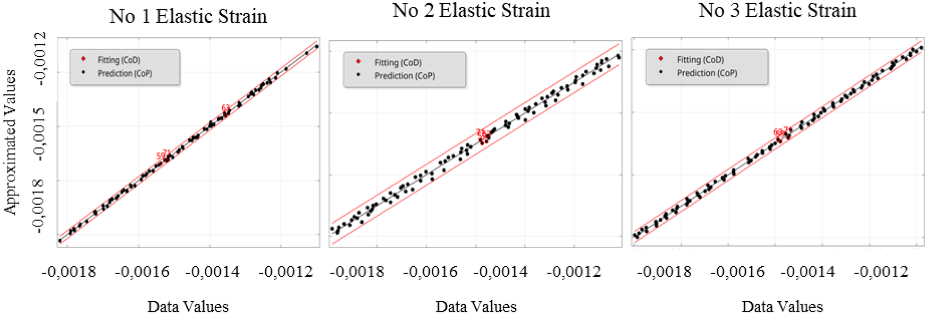
The median and deviation amounts of the response functions are given in Figure 20. Based on the figure, it was observed that the distributions were organized in a systematic way within the defined ranges. Median and deflection of response functions.
Printed circuit board optimization result
Parameters, only the clamp location in the Y-axis and the thermal expansion coefficient in the Y-axis, were considered in the optimization study. Due to the fact that, when the importance of all parameters from the experimental design results were examined, remaining parameters were decided to be insignificant. Based on the results of the experimental design, optimization targets were defined, and the best PCB design was obtained from the 500 estimated solutions. The best design is shown by a red line at the spider plot in Figure 21. Spider plot of regression model for optimization.
In Figure 22, the best design that fits the objectives is shown with the red dot in the three-dimensional Pareto diagram. The parameters and response functions of the best design are given in Table 5. 3D Pareto diagram of the optimization model. Design parameters and responses of best design.

Printed circuit board best design correlation
Design parameters and responses of best design.

Conclusion
In this study, a sensitivity analysis of PCBs was created by defining the strain values as responses and the material properties as design variables. The results of the sensitivity analysis were interpreted, and data analysis was performed using various statistical tools. According to the statistical data examined, unimportant design parameters were eliminated. The optimization model of the PCB was established, and the best design was obtained as a result of the solution. The finite element solution of the best design was compared with the physical test result, and the deviation percentage was given. Results were summarized below: • Maximum %5 error was seen between the thermal map measured with the thermal camera and the thermal map obtained by using the computer-aided software. • After the sensitivity analysis, it was seen that the thermal expansion coefficient in Y and the location of the clamp affected the response functions more than the other design parameters, so other parameters were eliminated. • When the accuracy of the regression was examined in the sensitivity analysis, it was observed that it was high (99.9%) and the deviations of the variables were very low. • The best design model obtained in the optimization was compared with the physical test, and it was seen that there was a maximum error rate of 9.4%. • By calibrating the PCB material properties in the FEA, the stresses on the solder leads were calculated more accurately. As a result, failures such as solder cracks that may occur during the design phase are prevented.
This study is promising for the automotive lighting community and for the industries working with PCBs affected by design parameters such as material properties or boundary conditions, due to the following reasons: 1. There are many design variables, such as the material properties of dozens of components on the PCB, the thickness of the composite layers, and the types of solder leads. Sensitivity analyses or optimizations of these variables can be performed with low error rates using the method in this study. 2. Response functions such as stress on solder leads or fatigue life in PCBs can be considered as different fields of study.
Footnotes
Declaration of conflicting interests
The author(s) declared no potential conflicts of interest with respect to the research, authorship, and/or publication of this article.
Funding
The author(s) received no financial support for the research, authorship, and/or publication of this article.