
Abstract
Smart materials have an important role in modern applications. They have contributed to improving various applications in several fields. One of the areas most affected by the improvement of smart materials is nanostructures. These materials are created by basic techniques, such as arrangement manipulation. Significant efforts have been made to enhance smart materials so that they resemble natural materials in terms of accuracy, design, and utility. Here, a review of the latest research on smart materials that can alter the electrical properties of nanostructures is presented. The main objective of this review is to introduce the role of smart materials in controlling the electrical performance of nanostructures. Furthermore, this review proposes an analysis of the integration and cooperation of previous research, such as the use of a piezoelectric motor in the design of structural magnetic nanodevices to control these devices. Piezoelectric actuators can also be used to develop a new method for controlling PV modulators for fabricating a single-wall nanotube. This new proposal could alter the properties of many nanoscale systems serving several medical and engineering fields. Moreover, this review proposes a novel methodology for nanocoating by introducing an antireflective coating with multiple layers. This method can effectively enhance the functions of the nanoscale coating.
Keywords
Introduction
Smart materials have become an indispensable part of progress in many areas. They have significantly contributed to the development of several applications in various fields, such as telecommunications, engineering, medicine, science, and agriculture. Smart materials are distinguished by having several characteristics that change under the influence of an external effect, such as pressure, heat, and an electrical field and are continually reacted based on the type of external impact. One of the areas most affected by the development of smart materials is nanostructures, which are materials or structures that have at least one dimension between 1 nm and 100 nm. Nanostructures are fabricated by methods as simple as solution processing and as complicated as advanced. Major efforts have been undertaken to create increasingly sophisticated materials that begin to mimic biological materials with respect to precision, architecture, and functionality. Combinations of theoretical and experimental methods will significantly widen the design parameters available for smart materials. 1
Notwithstanding the broad efforts in the manufacture of nanostructures, innovative work into nanostructures similarly centers around examining their essential material properties. This work includes mechanical, electrical, and optical properties at the nanoscale and the improvement of novel applications in a wide scope of designing fields. 2,3 Thus, we shed light on the most recent research on smart materials, the electrical properties of which change, and the effect of these developments in nanostructure applications. There are six types of materials that can change the electrical properties of nanostructures. Piezoelectric materials can produce a voltage when stress is applied. Photovoltaic materials or optoelectronics convert light to electrical flow. Electroactive polymers change their volume by voltage or electric fields, and electrochromic materials alter their shading or obscurity due to the use of a voltage. Dielectric elastomers produce extensive strain that is affected by an outside electrical field, and thermoelectric (TE) materials are utilized to construct gadgets that convert temperature contrasts into power and vice versa. 4,5
Smart materials are significantly altered in a manner that is controlled by outside stimuli, such as pressure, moisture, electrical power, magnetic fields, mild, temperature, or chemical compounds. Due to these vital properties of smart substances, the efficient use of such materials directly influences the electrical properties of the microstructure. This review aims to introduce how smart materials can convert the electrical properties of the nanostructure. Additionally, it focuses on the significance of antireflective coating in nanostructures. This assessment proposes a reconceptualization concept to approximate the probability of obtaining beam trajectories with distinctive orientations within the context of using the generation of antireflective coating with multiple layers. It is often used to generate a nanocoating.
Previous efforts suggest the necessity of making and self-destruction capabilities of nanostructures and nanocomponents. These smart materials can transform the stimuli into various types of energy and perform beneficial reactions. In addition, changing electric conductivity to sense or generate electrical nanofeatures and components is an important trend in designing the nanoscale features of nanostructures. For example, the electrical conductivity of the material could be decreased in its nanostructure, leading to new types of sensors, motors, wires, and electrical devices that are fabricated in nanoscale with an amazing electrical–mechanical property. This new property can change and enhance their tasks and their conductivity. Furthermore, the nanoscale programmable materials would furnish the components necessary for a new class of small-scale mechanical and electronic devices capable of carrying out any task. Based on this view about the future of smart materials in nanostructures, the first objective of this review is to introduce comprehensive details about recent research in this field. This review classifies these efforts into six categories based on the types of smart materials as follows: piezoelectric, photovoltaic, dielectric, electroactive, electrochromic, and TE materials. The second objective of this review is to propose an integration between recent efforts, such as the use of a piezoelectric motor in the design of structural magnetic devices. The piezoelectric actuator can be used to create a new technique for modulating the PV to produce a single-wall nanotube (SWNT).
This review is carried out as follows: The second section carefully describes the roles of piezoelectric substances in nanostructures. The third section discusses light control using photovoltaic materials. The fourth section gives the probability of acquiring a green modern-day compound with dielectric elastomers. The fifth section introduces the occurrence of electrical fields using electroactive polymers. The sixth section demonstrates the techniques of applying energy to the use of electrochromic materials, and the seventh section introduces methods of generating strength through TE materials.
Piezoelectric materials in nanostructures
Piezoelectric materials generate electrical load from applied mechanical loads. Because they can directly convert mechanical power to electricity, these materials have become the most important functional material in smart structures for sensors and actuators, and vice versa. They have excellent electromechanical coupling properties and impressive frequency response. Due to the enhanced piezoelectric properties, exceptional mechanical properties, and tunable electrical properties, single-dimensional piezoelectric materials have shown promising applications in nanogenerators, sensors, actuators, and electronic devices. Piezoelectric electrospun polyvinylidene fluoride (PVDF) nanocomposite films are made by an action tossing procedure in Fortunato et al. 6 Most of the research is based on zinc oxide because its nanostructures can be easily manufactured at low temperatures, 7 in comparison to many ferroelectrics, which require high temperatures. Furthermore, no poling is required because the nanostructures are crystallographically aligned and non-ferroelectric. Other well-known materials, such as lead zirconate titanate and barium titanate, have recently been investigated for nanostructured energy harvesters, with higher piezoelectric coefficients and the potential for increased power outputs. 8 Nanostructured piezoelectric energy harvesters have been developed from early reports of piezoelectric development from single-strained zinc oxide (ZnO) nanorods to include nanorod arrays, flexible substrates, and alternative materials and nanostructures. Crystallographically aligned ZnO nanorod arrays can be extended on a variety of substrates using low-temperature chemical synthesis methods. However, nanostructures of ZnO have been formed and used for energy harvesting in a small number of studies due to the use of various chemical compositions or substrate materials. When the same zinc nitrate-HMT chemical method was used to make nanorods on an aluminum-coated polyethersulfone substrate, contact with the Al surface produced ZnO nanosheets. 9 In addition, a sensor with a lone cathode piezoelectric nanogenerator made with PVDF nanofibers is presented in Wang et al. 10 The concepts of wavy-substrate self-fueled sensors and the 3D designs of Near-field electrospinning (NFES) PVDF micro/nano fibers (NMFs) with a 3D-printed custom-fitted substrate are introduced in Fuh et al. 11
The strategies of field-release separating electron microscopy, atomic power microscopy, and imperativeness dispersive x-bar examination are used in Fortunato et al. 12 Furthermore, powder X-bar diffraction, X-pillar photoelectron spectroscopy, and photoluminescence spectroscopy are used to make nanostructured films in Fortunato et al. 12 Nanostructured thin films are frequently used as photoactive self-cleansing fibers. The most popular technique is the self-cleaning of cotton with the use of a low-temperature sol–gel method. The nanocrystalline anatase titanium oxide (TiO2) was synthesized through colloid hydrolysis and, therefore, the extraction of titanium tetraisopropoxide. Cotton fibers were treated with colloid, wherein a thin film of anatase TiO2 became shaped on the surface of the fibers with the aid of a preferred coating process. In die-sensitized sun cells (DSSC), the semiconductor oxide thin film of TiO2 contributes to the insertion of coloration with its mesoporous characteristic. The stable pore architecture enables the electron switch and electron–hole interface to be grown effortlessly from the die to the collector electrode. Thin films of nanocrystalline TiO2 and porous silicon have been found to be suitable candidates for use in energy, catalytic, and optoelectronic devices. Thanks to the mineralization capability of pollutants, TiO2-coated fabric can provide self-cleaning surfaces, and TiO2 thin films are utilized in wastewater treatment. By facilitating coloration insertion and delivery of electrons, TiO2 thin films significantly increase DSSC efficiency. TiO2 thin film-mediated photocatalytic and photoelectrochemical water splitting can be an essential tool for producing hydrogen as a natural fuel. Porous silicon, on the other hand, has substantially contributed to the invention of electroluminescent devices, photonic crystals, and fuel and molecular biosensors. The use of nanocrystalline TiO2-loaded porous silicon films is now increasing for photocatalysis, solar cells, and gas sensing. 13
The piezoelectric response of the nanostructured films was reviewed through piezoresponse propel microscopy. 12 Indicator-based ℋ∞ control for piezoelectric nano stages with time postponements was introduced in Zhang and Peng. 14 A straight model with time delay and hysteresis valuation is discussed for piezoelectric nano stages, where the framework parameters are additionally chosen to utilize a distinguishing proof technique via the accumulation of trial information. 14 A controller is produced to accomplish robust solidness for the control of nano stages. A nonresonant-type piezoelectric engine with an exact driving capacity was exhibited in Xu et al. 15 Figure 1 depicts the basic structure of the piezoelectric motor.

Basic structure of the piezoelectric motor. 14
The working standard of the proposed engine is not the same as the past nonresonant piezoelectric engines utilizing either a bracing and supply tool or a latency drive mechanism. 15 A prototype motor is manufactured, and the machine to test the output characteristics is connected in Xing et al. 16 To simplify the driving power of the inertial drive piezoelectric motor, a low-frequency piezoelectric motor driven via a 50 Hz sine wave is proposed in Wang et al. 17 A linear piezoelectric motor using a hole rectangular stator that can translate a load positioned inside it by a direct drive is suggested in Izuhara and Mashimo. 18 A prototype motor is outlined in Cao et al. 19 with optimized parameters. Frequency response characteristics, displacement, and electromechanical coupling coefficients were calculated and compared with a finite element approach; the experimental results verified the model’s impact. Alumina was used in Wu et al. 20 to replace the metal components of the alumina, allowing the transducers to produce excessive torque and output energy of the rod-shaped piezoelectric rotary motors. Density functional theory was employed in Neto et al. 21 to simulate the molecular electronics behavior of the nitrogenous bases of human DNA under electric area effects.
A bond chart displaying the kinematic and dynamic qualities of a piezoelectric-activated smaller scale/nano material is provided in Lin et al. 22 This model can provide a convincing arrangement while investigating a small scale/nano framework. Magnetoelastic coupling in nanostructures and some suggestions for the structure of strain-controlled magnetostrictive nanogadgets are introduced in Foerster et al. 23 Powerful mechanical properties of multilayer nanoheterostructures were created in Mukhopadhyay et al., 24 where effective shut structure articulations for the equally versatile properties of such multilayer hexagonal nanoheterostructures are exhibited. Nanopillar electron diffraction in examining transmission electron microscopy mode has been utilized, with measurements performed for the incited piezoelectric fields in a GaN/AlN in Carvalho et al. 25 A strategy for incorporating segregated piezoelectric nanomaterials to relax the clipping power and recuperate unique piezoelectric properties of the materials is presented in Kang et al. 26 Poly (vinylidine fluoride–trifluoroethylene) (P (VDF-TruFE)) may be a special polymer that routinely paperwork the ferroelectric active beta phase without mechanical orientation. For packages that use the coating process, it is crucial to use a thin layer piezoelectric active fabric at the surface, such as a spin coating on silicone film, roll-to-roll printing, or screen printing on a plastic surface. Vertically adjusted P(VDF-TrFE) center shell structures utilizing high modulus polyurethane acrylate columns as the assisting structure to maintain the auxiliary nature of a material was produced in Choi et al. 27 The main utilization of a two-dimensional (2D) ZnO nanostructure and an anionic nanoclay layer to create piezoelectric DC yield control is presented in Kim et al. 9 2D materials are crystalline compounds that incorporate one layer of atoms. These substances are utilized in packages such as photovoltaics, semiconductors, electrodes, and water purification. It is feasible to assemble photonic gadgets using heterostructures containing slim hole block phosphorus and significant gap transition metal dichalcogenides (TMDCs). The electronic mobility of 2D substances and 2D heterostructures enable their use in optoelectronic and electronic devices: bodily phenomenon and device programs. Heat-discharge nanocircuits can be formed via 2D systems, electrical and mechanical devices derived from 2D materials, and consequently the environment. Magnetic tunnel junctions, the optoelectronic phenomenon, device applications, and other packages such as microwave, millimeter-wave, and terahertz (THz) gadgets have emerged. Additionally, nonstop scaling and microelectronic miniaturization of transistors may have significant utility in nuclear membrane materials. 28
Photovoltaic materials and light control
The single-dimensional organic–inorganic structure of nanostructures in photoelectric applications has attracted substantial attention worldwide. There are important implications on the study of nanoscale electronics as well as inorganic nanomaterials. In contrast, semiconductor organic–inorganic hybrid nanowires (NWs) are increasingly of interest due to their improved photoelectronic and photocatalytic cells. This focus was inspired by the theoretical principles described in photonic applications of hybrid semiconductors. A light administration strategy is proposed and, after that, streamlined by increasing size, design, or materials of nanoresonators. 29 Specially designed semiconductor nanoparticles are used as photo-anodes and have dimensions under 20 nm, which enable photosynthesis to take place while allowing electrons to pass through the nanofilms without interfering. For the purposes of studying charge transport, it is common to use the random walk model, but it applies to electrons instead. TiO-based photoanodes are a topic of significant interest. Multiple strategies may be employed to create TiO2 NWs; TiO2 nanotubes (NTs) have been produced using sodium surfactantide nanoparticles as a mold. A single diameter anatase TiO2 nanoparticle has been fabricated with outer and inner diameters of 10 and 500 nm, respectively, using the latest techniques. 30 A design of nanoresonator clusters consolidating various materials, including silicon dioxide, silicon nitride, and titanium dioxide that increases light retention, was additionally recommended in Ha and Zhitenev. 29 A new approach for measuring the relative quantum performance of a photodiode has been proposed by evaluation with a pyroelectric detector, which requires at least one-nanosecond laser pulses. The most important advantage of this technique is that an immediate comparison with an outsized distinction between the two detectors is feasible with a relatively simple setup. The spectral mirrored image of a pyroelectric detector can be a widespread reference for relative quantum performance.
This technique is useful for increasing knowledge regarding the quantum efficiency scale of optical detectors. 31 This methodology has been shown for Si and Ge photodiodes at a wide wavelength range. A natural electrochemical transistor was coordinated and utilized as a sensor with natural photovoltaic power sources on a one-micrometer-thick ultra-adaptable substrate in Park et al. 32 Figure 2 depicts a schematic of a double-grating-patterned organic photovoltaic. Nanostructures are framed on tips and pits, and a level surface is displayed utilizing a dry drawing strategy and a wet carving technique. Nanostructures scratched by the wet drawing strategy (13 µm) were taller than those carved by the dry drawing technique (1 µm). 33 A sort of self-fueled UV photodetector was structured utilizing single-crystalline ZnS NTs as the photodetection layer and Ag NWs arranged as straightforward cathodes. 34 A nanocrossover photocatalytic get together is accounted for in Pavliuk et al., 35 enabling corresponding reductive hydrogen creation and toxin oxidation with the sun oriented to allow for fuel efficiencies up to 20%. The neighborhood photovoltaic and photoconductive properties of 71° area dividers on BiFeO3 slight films with nanoscale goals are described in Yang et al. 36 Some progressed methods have been utilized, including synchrotron-based touching occurrence X-beam diffraction to observe precious stone structures and the concoction change of perovskites. 37 Basic wet anisotropic carving was created to manufacture various leveled silicon nanostructured clusters, with various sun-oriented cell contact configurations, trailed by efficient examinations of their photovoltaic attributes. 38 Expansive territory germanium tin nanometer insufficient films developed on highly adaptable aluminum foil substrates utilizing low-temperature subatomic shaft epitaxy were shown in Jin et al. 39 The improved and controllable reaction in MoS2 by using surface plasmonic reverberation was dependent on a metallic nanoreceiving wire with a trademark horizontal size of 40 × 80 nm2. 40 A completely new localized surface plasmon resonances (LSPRs) approach is proposed for fitting lateral photovoltaic effect (LPE)-based gadgets and, furthermore, opening research avenues into the momentum photoelectric sensors region. 41 Auxiliary electron location can be utilized to acquire high-distinguished material-explicit images of a natural photovoltaic mix. 42 Leaf surface bio-mirroring can be considered as a key title to outline fronts of light gathering frameworks. 43

Schematic of a double-grating-patterned organic photovoltaic. 32
Efficient electrical energy with dielectric elastomers
Nanotechnology-based dielectric elastomer transducers are used for a growing number of applications. These glasses have a high refractive index. The key here is that sub-wavelength light can be controlled to produce the desired results. This system consists of nonconductive soft membranes. They show unique performance characteristics (i.e. they actuate in a similar manner to human skeletal muscles, and they respond like human skeletal muscles). The electrostatic pressure in polydimethylsiloxane (PDMS) drives the incompressible elastomer to expand by tens of percent. The two main ways to increase the compliance of an electrode are the addition of wrinkles to the metal surface and by adding materials that change the stress in the metal and the substrate. A solid manufacture procedure is presented in Tan et al. 44 to exchange high-goal metallic structures of <500 nm in the measurement of elastomers.
Styrene (St) and acrylic acid were purified using vacuum distillation (AA). The receptor was extracted by washing n-butyl acrylate (nBA) with a 10% sodium hydroxide aqueous solution. Potassium persulfate (KPS, >99%), hydrochloric acid (HCl, 37 wt%), and sodium hydroxide (NaOH, >96%) were used without further purification. A protocol 45 was used to make the oligo (acrylic acid-b-styrene) trithiocarbonate macroRAFT agent (AA20-bSt5-RAFT agent). According to the 1H NMR spectrum, a macroRAFT agent molecule had 20 AA and 5 St units. GPC 46 determined the relative molecular weight of the AA20-b-St5-RAFT agent to be 2309 g/mol. Nanoparticles of TiO2, smoldered silica, and silaned silica added to a silicone-based elastomer utilized for the manufacture of maxillofacial prostheses were found to be nontoxic. 47 Monodispersed polystyrene particles, with distances in the scope of many nanometers, were infused onto the stretched film. Furthermore, a close-pressed monolayer of particles was self-collected and connected on the best surface of the film because of its viscidity. 48 An atomistic subatomic demonstration was utilized to recognize a novel nanomechanical component for dissipative issues in silica-filled elastomers when the latter are exposed to dynamic strain. 49 Surface coatings were utilized to produce uniform chief fields in nematic fluid precious stone elastomers. 50 Mechanically strengthened skin hardware was introduced by using organized nanocomposite elastomers in Han et al. 51 The impact of including diverse centralizations of surface-treated silicon dioxide (SiO2) nanoparticles on clinically critical mechanical properties of a maxillofacial silicone elastomer was investigated in Zayed et al. 52 The impact of the fusing of two regulations of nanooxides on the shading solidness of inherently hued silicone elastomers subjected to outdoor weathering is assessed in Akash and Guttal. 53 A profoundly adaptable, stretchable strain sensor was accounted for in Amjadi et al. 54 that was dependent on the nanocomposite of a silver NW system and PDMS elastomer as the sandwich structure. The impact of TiO2 nanoparticles on the biomechanical properties of a medical silicone elastomer is assessed in Wang et al. 55 A NT fluid gem elastomer was shown, and a remarkable and reversible photomechanical reaction was introduced for this layered composite to excitation by close infrared light at ultralow NT mass portions. 56 Printing practical protein nanodots on delicate elastomers is proposed in Alameddine et al., 57 where submicronic protein designs are first framed on glass and then imprinted on to an elastomer. Optical spectroscopy information of the light change process is merged with the nano plainly visible viscoelastic image of the host material inserting dynamic colors is introduced in Monguzzi et al. 58
Various electric fields using electroactive polymers
Electroactive polymers have gained some attention for their energy storage, sensing, and separation applications. The polymers have electrically active groups. The union of nanostructures and electro-responsiveness has shown strong potential in the design of next-generation energy storage devices, sensors, catalysts, and separation platforms. The interactions between the polymer and target molecules determine the electroactive materials’ performance. Nanostructures reduce the diffusion path of electrolyte ions or target molecules. This approach allows for the efficient use of polymeric materials.
An upgraded electromechanical implementation of TiO2 nanomolecule-altered PDMS as electroactive polymers is introduced in Ouyang et al. 59 A multifunctional stage dependent on electroactive polymers and silica nanoparticles for tissue building applications is presented in Ribeiro et al. 60 The effective dielectric thickness was reduced with the addition of an electroactive polymer. Based on the findings that the outputs do not increase proportionally, the changed material and secondary nanostructure on the surface tend to have a higher impact on efficiency than the increase in thickness. The electrospun contact surfaces’ rough PVDF nanofibers have a lower contact area than the triboelectric pair of polytetrafluoroethylene (PTFE)/PVDF/EVOH composite nanofiber membranes (PPECNMs) with a secondary nanostructure. The production performance of PECNM-triboelectric nanogenerators (TENGs) was optimized for the following applications because of the two-layer coating. PTFE has the highest tendency to gain electrons due to the triboelectric series, allowing for increased performance efficiency. The PTFE emulsion was proportionally applied to a PVDF solution for non-solvent-mediated phase separation. The maximum output voltage and current of PPECNM-TENGs were 145.5 V and 30.04 A, respectively. PTFE particles are contained in the pores of PVDF nanosheets. 61
An extremely quick and stable ionic electroactive polymer was created in Park et al. 62 by a nanocomposite that included poly(3,4-ethylenedioxythiophene):polystyrene sulfonate (PEDOT:PSS) and graphene−Ag-NWs (P/(G−Ag)). An investigation on the advancement of carbon NT-based composite actuators is introduced in Chen et al., 63 utilizing another ionic fluid-doped electroactive ionic polymer. Ongoing advances in the creation and use of nanocomposite hydrogels in tissue design applications are shown in Mehrali et al., 64 with explicit consideration toward skeletal and electroactive tissues; for example, heart, nerve, bone, ligament, and skeletal muscle. Elite electroactive polymer actuators are discussed in Wang et al. 65 that are dependent on ultrathick ionic polymer-metal composites with nanodispersed metal terminals. The combination and portrayal of an injectable hydrogel was examined in Wang et al. 66 and depends on oxidized alginate (OA) cross-linking gelatin fortified by electroactive tetraaniline-join OA nanoparticles for biomedical applications. A strategy for the integration of electroactive polymers is shown in Cantu et al., 67 beginning with the combination of broad coupling monomers utilizing a three-advance procedure completed with Negishi coupling. These electroactive polymer nanoparticles show photothermal properties, as introduced in Cantu et al. 67 Adaptable poly PVDF-based nanocomposites containing Au and Cu-doped graphene oxide (GO/Au and GO/Cu) nanosheets were established by a procedure introduced in Fakhri et al. 68 The impact of two nanofillers and the utilization of five unlike hexahydrate salts on the nucleation of the electroactive stage in solution-derived PVDF films are outlined in Chandraiahgari et al. 69 Electroactive qualities of BNNTs in novel multifunctional electroactive nanocomposites have been presented in Kang et al. 70 Electroactivity and geological stimuli given by TMV/PANi/PSS nanofibers can synergistically animate neural cell separation and neurite outgrowth, which make it a promising framework material for neural tissue design. 71 Another electroactive actuator comprising self-amassed sulfonated square copolymers and ionic fluids utilizing nanostructured polymer electrolytes is discussed in Kim et al. 72
Methods of applying energy using electrochromic materials
The electrochromic phenomenon describes how the optical properties of a material change with an applied voltage. Nanostructures for electrochromic materials include ultrathin crystalline NTs, NWs or NTs, crystalline mesoporous structures, and quantum dots. Large, specific surface areas are expected to produce fast and stable electro-channels. Synthesis methods are favorable for these nanostructures. To produce a transparent electrochromic film on a conductive substrate, a special coating process must also be developed. These coatings were electrodeposited in nickel nitrate (90% aqueous nitrate, 0.04 mM Ni (NO3)2). Depositions were rendered at a height of 4 cm2 above the substrate level on an FTO/glass. Prior to electrodeposition, the substrates were treated with ultrasound, acetone, and ethanol for 10 min. A three-electrode cell was used to deposit the material, with a saturated calomel as the working electrode (SCE). While the platinum was in contact with the substrate, the counter electrode was attached to the working electrode. The films were washed, dried, and annealed at 300°C for 1 h to obtain NiO films from electrodeposited Ni (OH)2OH films. 61
A high-rendering, flash-induced AgNW network-based transparent conducting electrode (TCE) on surface-treated (PDMS) substrates is introduced in Lee et al. 73 A Xe streak light plan was utilized to make nanowelded silver NW systems. Highly effective, close infrared, and noticeably light-tweaked electrochromic gadgets dependent on polyoxometalates and W18O49 NWs are presented in Gu et al. 74 NWs are crucial in digital, optoelectronic, and nanoelectromechanical devices, as components in sophisticated alloys, for metallic interconnects in nanoscale quantum devices, as subject-emitters, and for biomolecular nanosensors. Some NWs are exquisite conductors or semiconductors, and their minus length means that manufacturers can match many transistors on one microprocessor. As a result, laptop speeds can grow dramatically. NWs play a critical role in the field of quantum computers. NWs coordinate with the outside magnetic flux, and the foremost advanced NWs are formed through the coordination of the magnetic interaction. This process occurs among the nanomagnets at the NW and, therefore, the ferromagnetic pads on the surface.
NWs are primarily applied to sensors, such as pH and fuel sensors. NWs are frequently used for MOS area-effect transistors (MOSFETs), which are often used as simple structural elements in today’s electronic circuits. An arrangement stage union of 2D WO3 nanosheets through straightforward oxidation from 2D tungsten disulfide (WS2) can be used. Nanosheets peeled from mass WS2 powder are described as superior electrochromic gadgets in Azam et al. 75 A sound plan of a vigorous sandwich-organized nanofluidic diode was introduced in Zhang et al. 76 By making inverse charges on the outside surfaces of a nanoporous layer utilizing inorganic oxides with isoelectric points, the diode is additionally formed into an electrochromic film displaying a visual shading change considering redox potentials. 74 An optically adjusted electrochromic-intense gadget was created in Kang et al. 77 through successive evidence of crown-type polyoxometalates, K28Li5H7P8W48O184·92H2O (P8W48) and W18O49 NWs. A conductive nanopaper that transmits best-in-class electro-optical performance was accomplished with an adaptable nanopaper exchange strategy that encourages joint incorporating for outstanding electrodes in Kang et al., 77 and adaptable electrochromic supercapacitor (SC) cathodes utilizing novel adaptable straightforward substrates was created in Shen et al. 78 Manufacture of an SWNT slender film-based electro-optical modulator constrained by ionic fluid polarization was displayed in Moser et al., 79 in which the dynamic electrochromic layer was made of a film of semiconducting (SC-) SWNTs, and the counter-terminal comprised a film of metallic (MT-) SWNTs. A screen-printed dynamic framework electrochromic that utilizes carbon NT slender film transistors is presented in Cao et al. 80 Nickel–cobalt hydroxide on reduced GO can be used for adaptable electrochromic supercapacitors. It was demonstrated that rGO nanosheets are homogeneously covered with metal hydroxide and are vertically stacked. 81 The basic measurements in the nanocomposite are intended to upgrade pathways for electrochemical charging and release. 82 A plasmon dynamic nanomaterial configuration is displayed in König et al. 83 with electrochemical tunability of the confined surface plasmon resonances. Nanopolycrystalline WO3 dainty films with a thickness of 100–200 nm have been consistently arranged on the planned areas of indium tin oxide (ITO) glass substrates by warm dissipation representation in Luo et al. 84 Nanostructured NiO terminals demonstrated significantly upgraded electrochromic execution, joining fast exchanging rates with a high hue differentiate. 85 An adaptable electrochromic gadget is outlined in Liang et al. 86 that is dependent on effortless semiconductor-to-metal changes in WO3·2H2O ultrathin nanosheets.
Creating an electric potential via TE materials
TE technology has long been known as a potentially transformative energy generation technology. It is now growing steadily due to its ability to convert heat directly into electricity. Nanostructured materials have the most potential for commercial use due to their high TE performance. High-efficiency TE materials are an important technology for converting waste heat to electrical energy. TE properties depend on the sensitivity of the nanostructure, the synthesis approach used, and device assembly. Narrow bandages, heavy doping elements, point loading defects, and nanostructures will continue to be studied.
An upgraded TE execution of graphene-based nanostructures is introduced in Hossain et al. 87 TE efficiency is examined for a one-dimensional topological superconductor, which has two Majorana fermion states at its edges. 88 To render TE composites, researchers used a polymeric matrix doped with carbon NTs and other nanoscale fillers. A repeating unit-cell can then be used to characterize the TE composite material. When the specimen is subjected to directional heating or cooling for nondestructive research, the high-sensitivity superconducting quantum interference system magnetometers can detect the weak TE currents around the inclusion region. Micro models for multiphase periodic thermoelectrical composite materials and devices are developed using typical continuum models. A fully coupled micro thermo-electric module (TEM) formulation is required for periodic multiphase TE material systems. When applied to similar problems involving nanosized structures, classic electromechanical coupling theories, on the other hand, fail to describe the size-dependent phenomenon observed experimentally. 89
It may be utilized for precise temperature detection at the nanoscale. The principal TE properties of single-walled carbon nanotubes (SWCNTs), NT-based composites, and TE gadgets arranged from these materials are investigated in Blackburn et al. 90 It is demonstrated that the characteristic electronic properties of graphene strips can be completely recovered, and their TE effectiveness was clearly improved by methods for atomistic counts. 91 A nano Bi and Te molecule slurry are utilized in a screen-printing strategy to create n-and p-type TE intersection with Ag doping. 92 An upgraded TE execution of Cu2SnSe3-based composites joined with nanofullerene is presented in Zhao et al. 93 The high-temperature TE properties of high virtue Bi-doped Mg2(Si, Sn) are introduced in Farahi et al. 94 Plasma-wave, TE and bolometric nanofinders with a switchable and controllable working instrument are introduced in Viti et al. 95 The warm conductivity of GNRs is diminished by presenting pores in them to improve their TE execution, as introduced in Hossain et al. 96
The TE transport properties of p-type Bi2Te3 nanofilms with different quintuple layers (QL) were explored in Zhou and Wang. 98 These properties were dependent on monitoring the abdominal muscle for electronic structure estimations and Boltzmann transport conditions. The role of nanoscale imperfection that includes upgrading the TE execution of p-type nanostructured SiGe amalgams is shown in Bathula et al. 99 The TE properties of graphene nanostrips (GNRs) are examined in Hossain et al. 100 with fused nanopores (NPs) and presents a nanopore-building approach for improving their TE properties. The sizes of nano and microstructures for superior and unbending mass TEs are investigated in Wang et al. 101 A capacitor-release sintering with silver–nickel nanocomposite in the interconnection of TE generators is introduced in Lu et al. 102
The TE properties of numerous center shell NWs are researched in Zhou and Chen. 103 This case is verified by utilizing Green’s nonequilibrium capacity technique and atomic element reproductions. The execution of the TE module has been improved in Rathnakannan and Priya 97 by utilizing SWCNT for n-leg. Figure 3 depicts a simple TEM built by using two legs of the TE material. Another methodology has been created for the normal plan of the interfaces in TE materials by utilizing all-inorganic nanocrystals that fill in as a stick for mesoscopic grains. 104

A simple thermoelectric module (TEM) is built by using two legs of the thermoelectric material 97 (a) Schematic of thermoelectric module; (b) schematic of position of micro-channel.
Roles of smart materials in tuning the electrical performances of nanostructures
Electrical tuning has a fast-switching speed and a high degree of modulation and represents one of the most powerful tuning techniques available. Absolute compositional tuning of ternary ditelluride nanobelts, critical to the production of unrivaled low-dimensional materials/devices, is accomplished by suppressed phase separation. This approach may encourage new growth/manufacturing strategies for 1D-layered nanostructures that may offer unique properties not available in other materials. 105 The morphological properties of nanoparticles are strongly influenced by the tuning of electrical, optical, and photocatalytic properties. Cadmium sulfide (CdS) nanoflakes and CdS nanospheres were synthesized by a simple chemical route—there was a significant improvement in the electrical characteristics of CdS nanoflakes due to the modulation of the form. 106
Because of the selective dispersion of electrons and phonons across interfaces, the TE properties of hierarchical nanostructures can be improved relatively easily. To test TE properties, the solution-based method synthesizes the flower-like nanostructure of SnSe2, and the spark plasma sinter synthesizes the nanostructure into pellet form (SPS). Thermo-electric efficiency of the flower-like SnSe2 is higher than that of nanoplates and bulk equivalents. It provides an important method for enhancing the TE properties of SnSe2-based materials. 107 Polymorphic gallium is seen as a highly promising candidate for adaptive plasmonics and reconfigurable photonics applications (Ga). Gas sp-metal is generally accepted at room temperature to be a liquid metal. In addition to many other excellent properties of nanostructured gas, its six phases have a wide range of electrical conductivity and optical action tunability, with varying degrees of metallic character. The dielectric function of the many Ga phases 108 has been introduced and is related to the respective electronic structures. Manipulating oxygen-related impurities is a serious challenge for most TE materials, particularly those with nanostructures, because they typically result in TE performance degradation. 109 Hematite (alpha-Fe2O3) is one of the most promising cost-effective and stable anode materials for photoelectrochemical applications, and its performance, similar to other metal oxide transitions, is highly dependent on its electrical and defective properties. 110
Increased demand for clean energy has catalyzed the construction of new plants capable of generating electricity from renewable energy sources. One possible alternative is the use of TE materials that can use waste heat, water, and solar thermal energy to generate electricity. Improvements in the performance of such devices can be achieved through the synergistic development of composites made of an organic matrix filled with nanostructured TE materials. 111
Recent increases in efficacy and advancement of perovskite organohalide (PSC) cells have been critical in this regard. Nanostructures have a significant impact on the efficiency of the PSC because their inherent optical, electrical, and electrochemical properties vary. For transparent conductive oxide substrates, 0D nanoparticles (TNPs), 1D nanoparticles (TNWs) to 2D nanoparticles (TNSs) of different sizes, and different TiO2 electron transport layers (ETLs) are formed by a variety of organic solvents. Such layers feature improved optical clarity, which minimizes the loss of absorption of light. Compared to 0D TNP counterparts, PSCs built with 1D TNW or 2D TNS deliver better photovoltaic performance. This two-layer ETL film can simultaneously block photo-generated holes, improve electron extraction, and thus improve the performance of the PSC. 112 A comparison of electrical and thermal conductivity with the Seebeck coefficient of Sb2Te3 nanoparticles obtained from different ILs shows that the same IL (of which C4mmI was identified as the best solvent) had a strong effect on the thermo-electric properties of Sb2Te3 nanosized as-prepared compounds. The design guidelines 113 for ILs were published to provide a synthesis of performance-enhanced nanostructured TE properties.
Ferro-electrical polarization for tuning load transport characteristics is a fascinating physical phenomenon used in a wide range of optoelectronic devices. Ferroelectric materials have been used in flat geometry or in chemically manufactured nanostructures. The nanoporous ferroelectric semiconductor approach provides a new architecture with significant potential for highly efficient PEC devices for renewable energy applications. 114 The design of effective water oxidation photoelectrodes requires careful optimization of the morphology and structure of the photoactive material to improve electrical conductivity and balance the length of diffusion of the carrier with the distance of light penetration. Hematite-based photoanodes, with ideal belt gaps, may theoretically oxidize water at very high rates, but their performance is limited by low transport charges and low separation efficiency. 115 MOS2 micro/nanostructures are desirable for tuning electronic properties, for developing the necessary functionality, and for improving the existing performance of MOS2 multilayer devices. Electrical field-effect transistor tests made of prepared MoS2 nanoribbon arrays show new interesting features: efficiency and transfer characteristics suggest a severe drain source current correction, apparently due to parallel structures with multiple edge defect and p-type chemical doping of the MoS2 nanoribbon array of oxygen molecules. The ability to directly induce micro/nanostructures by femtosecond laser pulses, changes in properties, and new device characteristics of 2D materials has been shown to allow for new applications in MoS2-based electronic devices such as logic circuits, complementary circuits, chemical sensors, and p-n diodes. 116 Nanostructured ITO surfaces provide a rare and unusual combination of properties with a high surface-to-volume ratio. Previous studies, therefore, identified nanostructured ITO electrodes as potentially acceptable platforms for electrochemical biosensors, but there is still a lack of research regarding improving the preparation methods for these electrodes. 117
Solvent-free ion nanofluids (NFs) are exciting smart lubricants. The effects of NF structures on their physicochemical properties and lubrication have been investigated. Tribofilm nanostructures have been fully characterized to shed light on the lubrication mechanisms of the NFs. Newly synthesized NFs show outstanding lubrication efficiency and excellent electrical lubrication response. By feeding NFs to the friction field, the growth of a robust tribofilm consisting primarily of SiO2 nanoparticles and tribochemicals is accelerated. The tuning structures and functionalities of the boundary layers of various motion components are now available by customizing NF architectures and controlling electrical stimuli. 118 Table 1 shows a comparison of smart materials used for tuning the nanostructures’ electrical properties. The advantages and disadvantages of these materials in building nanostructure are listed in this table.
A comparison of smart materials used for tuning the nanostructures’ electrical properties.

Proposed antireflective coating with multiple layers
Several efforts have also been made in the manufacture of nanosheets, including Cu-doped GO, 119,120 2D WO3, 121,122 and rGO. 123,124 The authors believe that other types of alloys can be studied with several previous alloys, with their characteristics and possibilities being used. It is clear from the research presented in this review that the role of smart materials has yet to be fully realized in updating and changing the electrical properties of nanostructures. The current research is not only changing nanomaterials, but its impact will extend to nanosystems to include a substantial number of applications. These applications can serve many fields, such as engineering, medicine, and science.
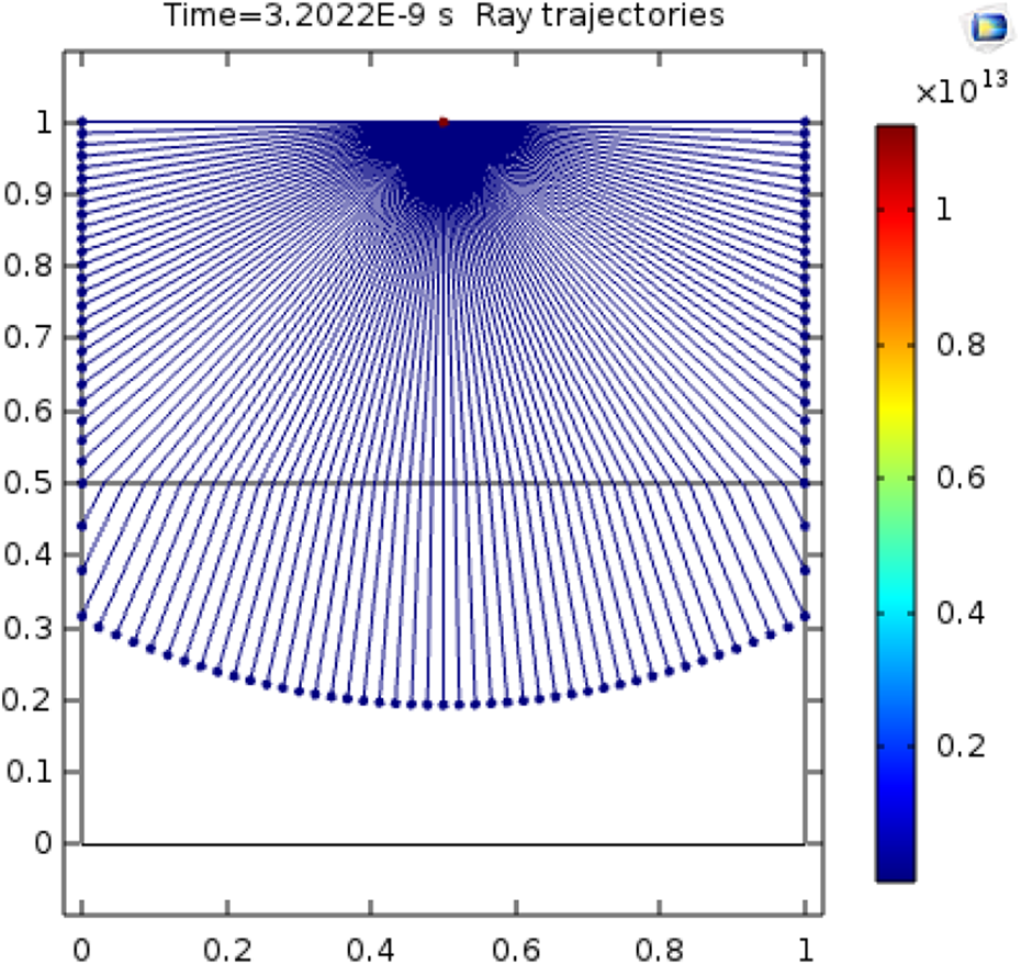
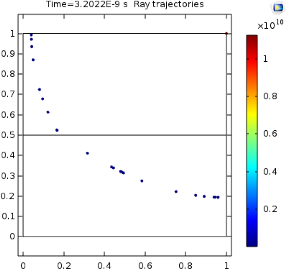
In this research, a COMSOL application was used to show the importance of antireflective coating in nanostructures. Figures 4 to 8 illustrate the possibility of obtaining ray trajectories with different orientations when using the antireflective coating technique with multiple layers. This approach can be used as an advanced technique in nanocoating to enhance the functionality of this type of coating. Figure 4 shows the ray trajectory calculations at a time of 3.6692e−9 from the starting point at zero. The figure provides a conical ray direction vector with random sampling from distribution. The number of rays in the wave vector space is 50, and the main ray frequency is 4.54e14 Hz. Figure 5 shows ray trajectory calculations at time 3.20220e−9 and the spherical ray direction vector with deterministic sampling from distribution with a 50-vector space and a mean ray frequency of 4.54e14. Figure 6 outlines the ray trajectory calculations at time 3.20220e−9 spherical direct vector with deterministic sampling from distribution with a 200-vector space and a mean ray frequency of 4.54e14 Hz. Figure 7 shows the ray trajectory calculations at time 3.20220e−9 spherical direct vector with random sampling from distribution with a 100-vector space with partially coherent polarization, and Figure 8 illustrates the ray trajectory calculations at time 3.20220e−9 spherical direct vector with random sampling from distribution with a 100-vector space at different specified contributions of ranges from 1:1000 with step one. Using multiple layers can accelerate and increase the functionality of the nanocoating process due to the range variation of the ray trajectories.

Conical ray direction vector with random sampling distribution and fifty vector space.

Conical ray direction vector with deterministic sampling distribution and fifty vector space.
Deterministic ray direction vector with deterministic sampling distribution and 200 vector space.

Spherical direct vector with random sampling distribution with 100 vector space.
Spherical direct vector with random sampling from distribution with 100 vector space at different specified contributions of ranges from 1:1000 with step one.
Conclusion
Smart materials have directly contributed to enhancing the electrical properties of the nanostructures of several modern systems in various scientific applications. This research has provided a detailed review of these smart materials and their effective impact in changing the electrical properties of nanostructures. To present the roles of the smart materials in the nanostructure, these roles were classified into six categories according to the physical nature of each material: piezoelectric, photovoltaic, dielectric elastomers, electroactive polymers, electrochromic, and TE materials. Furthermore, this review has presented the role of smart materials in controlling the electrical properties of nanostructures. We considered the necessity of using the piezoelectric motor in designing the magnetic nanostructured devices to control these devices and the use of the piezoelectric motor to develop a new method for controlling the photoelectric modulator to manufacture an SWNT. It is also possible to study the stability property of its potential use in colorfastness for intrinsically colored flexible silicone rubbers for the face and jaws; this method could also enhance the functionality of this type of coating. More research is required regarding electromagnetic polymers because the new technology of ionic polymers saturated with ionic liquids can be utilized to increase the electromagnetic polymer’s performance.
Footnotes
Acknowledgements
The author extends his appreciation to the Deanship of Scientific Research at King Khalid University for funding this work through Research Groups Program under grant number [GRP/265/42].
Declaration of conflicting interests
The author(s) declared no potential conflicts of interest with respect to the research, authorship, and/or publication of this article.
Funding
The author(s) disclosed receipt of the following financial support for the research, authorship, and/or publication of this article: This research was funded by King Khalid University—KSA, grant number [GRP/265/42] and the APC was funded by King Khalid University—KSA.