
Abstract
Background:
Potential induced degradation (PID) has recently been identified as one of the most important degradation mechanisms for silicon solar cells. It is widely considered that PID is closely related with the manufacture and application period of solar modules.
Methods:
In this study, the effects of diffusion sheet resistance on PID were verified and explained by testing the emitter doping profile, the minority carrier lifetime, the emitter saturation current, the electrical performance of different cells, and the PID process.
Results:
With increasing sheet resistance of cells, the depth and saturation current density of the emitter both decreased, and the cell efficiency increased, whereas the PID phenomenon became serious.
Conclusions:
It was found that higher sheet resistance or thinner P–N junction could lead to higher PID sensitivity. Therefore, more attention should be paid to PID phenomenon as the photovoltaic industry develops in the direction of high sheet resistance.
Introduction
Silicon solar cells, as the main component of solar energy, have been widely used recently due to their merits in terms of environmental friendliness and mature manufacture processes compared to other solar technologies. However, in the running of solar power stations, different failure modes arise according to complex operating conditions. Photovoltaic (PV) modules are generally exposed to voltage bias of several hundred volts with respect to module frames. Due to these high voltages, solar modules may suffer the so-called potential induced degradation (PID) that may lead to significant performance loss.1,2
There is still some debate on the mechanism of the PID phenomenon, in which the cells, as the main power-generation unit, are highly correlated. 3 In the production process of crystalline silicon cells, the emitter performance in the diffusion process has a direct effect on the cell electrical performance. However, the effects of diffusion techniques on PID are not yet clearly understood. In this paper, the effects of diffusion sheet resistance on PID were verified and explained by testing the emitter doping profile, the minority carrier lifetime, the emitter saturation current, the electrical performance of different cells, and the PID process. On this basis, the mechanism of the PID phenomenon was analyzed and is verified at the end of this paper.
Methods
Conventional P-type polycrystalline silicon wafers were chosen as the raw materials for our experiment. After cleaning and texturing, the wafers were divided into five groups of 50 wafers each. Adequate phosphorus was injected by constant-source diffusion in the diffusion and driving processes. Samples with sheet resistances of 70 ohm/sq, 80 ohm/sq, 90 ohm/sq, 100 ohm/sq, and 110 ohm/sq were produced at 850 °C, 830 °C, 815 °C, 800 °C, and 785 °C, respectively. The emitter doping profile of each sample after diffusion was recorded by a CPV21 capacitor voltage tester. The minority carrier lifetime was tested by a WT2000 minority carrier lifetime tester, and the emitter saturation current was measured by a WCT120 minority carrier lifetime testing system. Each silicon wafer sample was made into several cells by conventional cell technology on the production line. The cell electrical performance was tested by a Halm tester. The PID of each cell sample was tested by a PIDcon cell tester at 85 °C with a reverse voltage of –1500 V for 24 h. After the cell sample was made into small modules, the PID was tested in a double-85 testing box under the conditions of 85 °C, 85% relative humidity, and –1000 V reverse voltage. The testing data after 96 h were analyzed.
Results
Effects of different emitter sheet resistances on silicon cell performance
Figure 1 shows the depth–concentration curves of different emitter samples, in which the deposited phosphorus source concentration on the silicon wafer surface is 1 × 10²¹ atoms/cm3. As the doping concentration at the continuous phosphorus source surface is kept constant, phosphorus atoms can diffuse into the silicon wafer continuously over time at a defined temperature. Along with the increase of diffusion depth, the doping concentration decreases linearly, and the decreasing trend of phosphorus doping concentration slows down at about 1 × 10¹⁶ atoms/cm3 when the diffusion depth is more than 0.3 μm. The emitter sheet resistance increases with decreasing temperature, and the depth of the emitter decreases with increasing sheet resistance. Thus, the depth of the emitter is the largest when the sheet resistance is 70 ohm/sq and the junction depth of the emitter is the smallest when the sheet resistance is 110 ohm/sq.
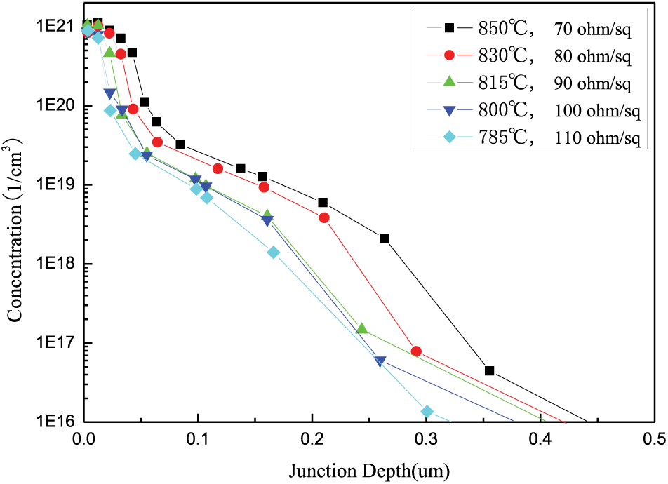
Depth–concentration curves of different emitters.
Figure 2 shows the variation in the minority carrier lifetime for the emitter samples with different junction depths at the same surface concentration. As can be seen, the minority carrier lifetime increases linearly from 16.17 μs to 20.53 μs when the sheet resistance increases from 70 ohm/sq to 110 ohm/sq. That is to say, the minority carrier lifetime increases with the increase of emitter sheet resistance, or with the decrease of emitter junction depth. The defect concentration at the silicon wafer P–N junction and the density at the recombination center increase with increasing phosphorus concentration. The recombination rate of the non-equilibrium carrier becomes faster, and thus the minority carrier lifetime decreases.
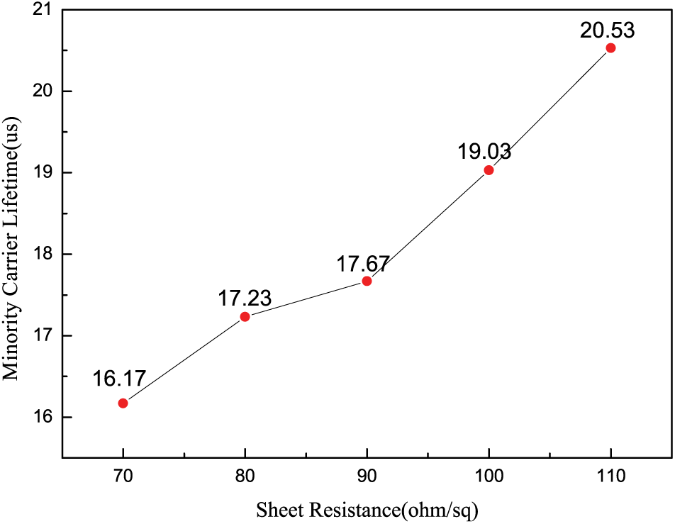
Variation of minority carrier lifetime with sheet resistance of different emitter samples.
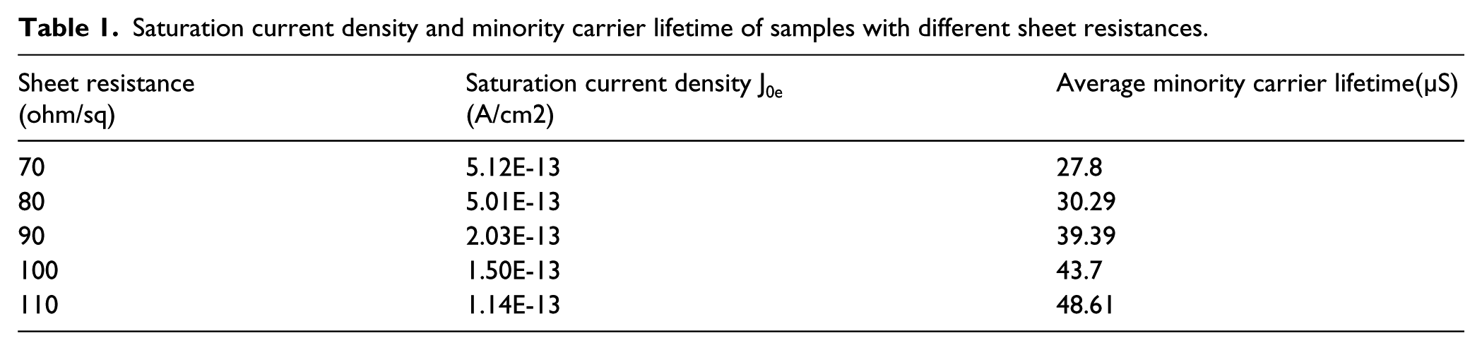
After SiN passivated film was deposited by Plasma-enhanced chemical vapor deposition (PECVD) on both faces of these five groups of samples with different sheet resistances, the emitter saturation current density and minority carrier lifetime were tested by the quasi-steady-state photoconductive minority carrier lifetime tester, as shown in Table 1.
Saturation current density and minority carrier lifetime of samples with different sheet resistances.
Emitter saturation current density is a parameter that combines the bulk recombination of the emitter with the recombination of the highly doped surface, which provides a good method to describe the diffusion layer recombination. Figure 3 shows the variation trends of the saturation current density (Joe) and minority carrier lifetime with the sheet resistance. It can be seen that the minority carrier lifetime increases from 27.8 μs to 48.6 μs with the increase of sheet resistance from 70 ohm/sq to 110 ohm/sq, which is consistent with the testing result shown in Figure 2. After the double-faced SiN passivates the silicon wafer, the hydrogen atoms in the SiN film can combine with the dangling bonds on the silicon wafer surface. As a result, the recombination centers at the silicon surface decrease greatly, and the minority carrier lifetime becomes longer than that before SiN passivation. On the other hand, the saturation current density of the samples with different sheet resistance Joe increases as the sheet resistance decreases, which is opposite to the variation trend of the minority carrier lifetime. Thus, the decrease in minority carrier lifetime can be explained by the increase of saturation current density.
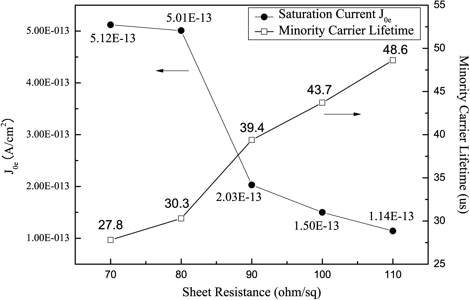
Variation trends of saturation current density J0e and minority carrier lifetime with sheet resistance.
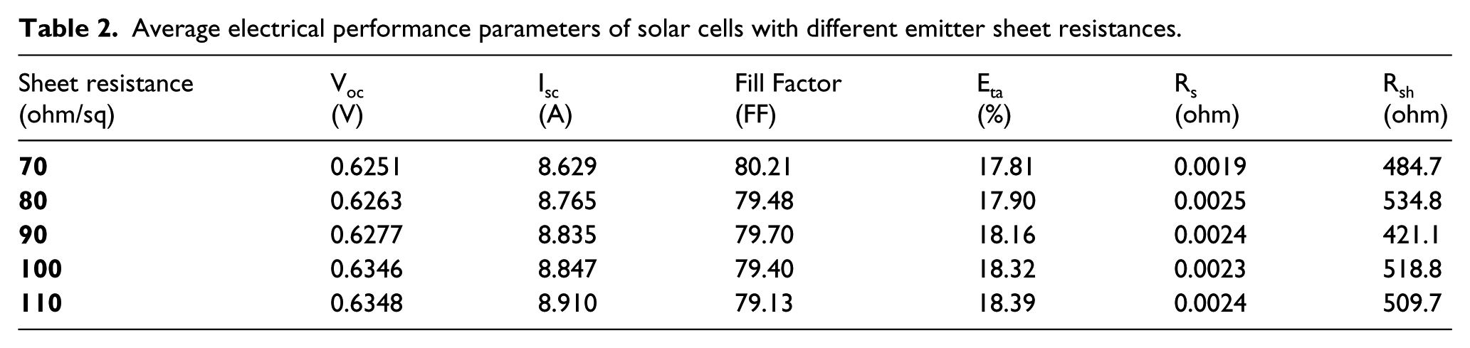
Figure 4 shows the variation trend of solar cell efficiency with different emitter sheet resistances, and Table 2 provides the average values of electrical performance parameters for different emitter cells. It can be seen that the open-circuit voltage, Voc, the short-circuit current, Isc, and the cell efficiency, Eta, all increase gradually with increasing sheet resistance. When the sheet resistance increases, the junction depth and the doping concentration at the same junction depth both decrease; the minority carrier lifetime increases and the emitter saturation current Joe of the P–N junction decreases. As a result, the Voc, the Isc, and the Eta all present an increasing trend.
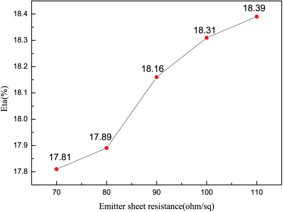
Variation trend of solar cell efficiency with emitter sheet resistance.
Average electrical performance parameters of solar cells with different emitter sheet resistances.
Effects of different emitter sheet resistances on the PID process
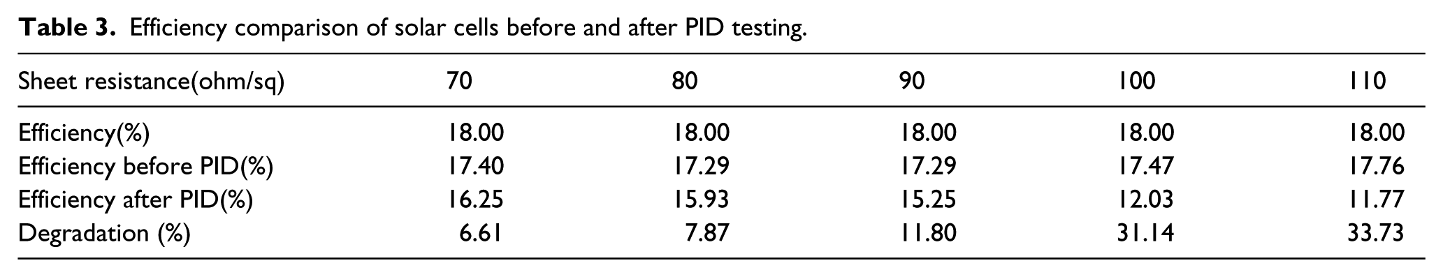
Five pieces of 300 mm × 300 mm modules were made by cells at the same cell efficiency with different sheet resistances of 70 ohm/sq, 80 ohm/sq, 90 ohm/sq, 100 ohm/sq, and 110 ohm/sq, respectively. The surface and the glass margin of these modules were packaged by aluminum foil, and then tested for 96 h in a double-85 environmental testing box under the conditions of 85 °C, 85% relative humidity, and –1000 V reverse voltage. The efficiency and degradation ratio of the cells before and after PID testing are shown in Table 3. Figure 5 shows the variation trend of PID with emitter sheet resistance of solar cells. As can be seen, the PID increases slowly from 6.61% to 7.86%, or by 1.25%, when the sheet resistance increases from 70 ohm/sq to 80 ohm/sq. It increases rapidly from 7.87% to 11.8%, or by 3.93%, when sheet resistance increases from 80 ohm/sq to 90 ohm/sq. It increases linearly from 11.8% to 31.14%, or by 19.6%, when the sheet resistance increases from 90 ohm/sq to 100 ohm/sq. When the resistance increases from 100 ohm/sq to 110 ohm/sq, the PID increases slowly. These results indicate that the doping concentration of phosphorus atoms decreases gradually with increasing sheet resistance. Meanwhile, the gettering ability of metallic ions in the bulk silicon and the passivation result of dislocation defects decrease with the decrease of doping concentration. Otherwise, the metallic ions and dislocation defects increase with the increase of sheet resistance. The gettering ability and passivation ability are weakened with the increase of sheet resistance from 70 ohm/sq to 90 ohm/sq, thus enhancing the PID effect. When the sheet resistance increases from 90 ohm/sq to 100 ohm/sq, the junction of doped atoms is shallow, and the gettering and passivation abilities of phosphorus atoms decrease quickly, thus significantly enhancing the PID effect. When the sheet resistance increases from 100 ohm/sq to 110 ohm/sq, the gettering and passivation abilities of phosphorus atoms are weakened slowly, which leads to a slow decrease of the PID effect.
Efficiency comparison of solar cells before and after PID testing.
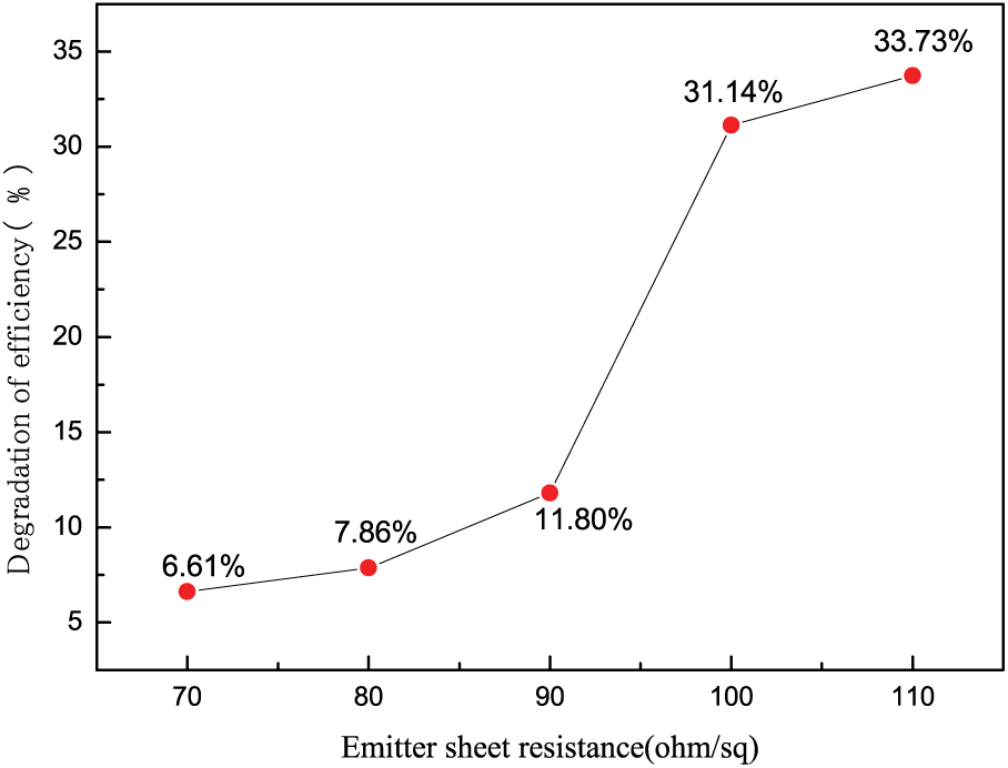
Variation trend of PID with sheet resistance of solar cells with different emitters.
Figure 6 shows the degradation variation rule before and after PID testing by Electroluminescence (EL) testing. Before PID testing, the EL images seem bright. After PID testing, the dark areas of the EL images increases with the increase of sheet resistance. When the sheet resistance is 70 ohm/sq, the dark areas of the EL images after PID testing is small; when it increases to 110 ohm/sq, the dark areas of EL images become larger; afterwards, the spectral response of EL testing is weakened and most areas of the EL images become dark. These results explain that higher sheet resistance of cells can more likely induce the PID phenomenon.
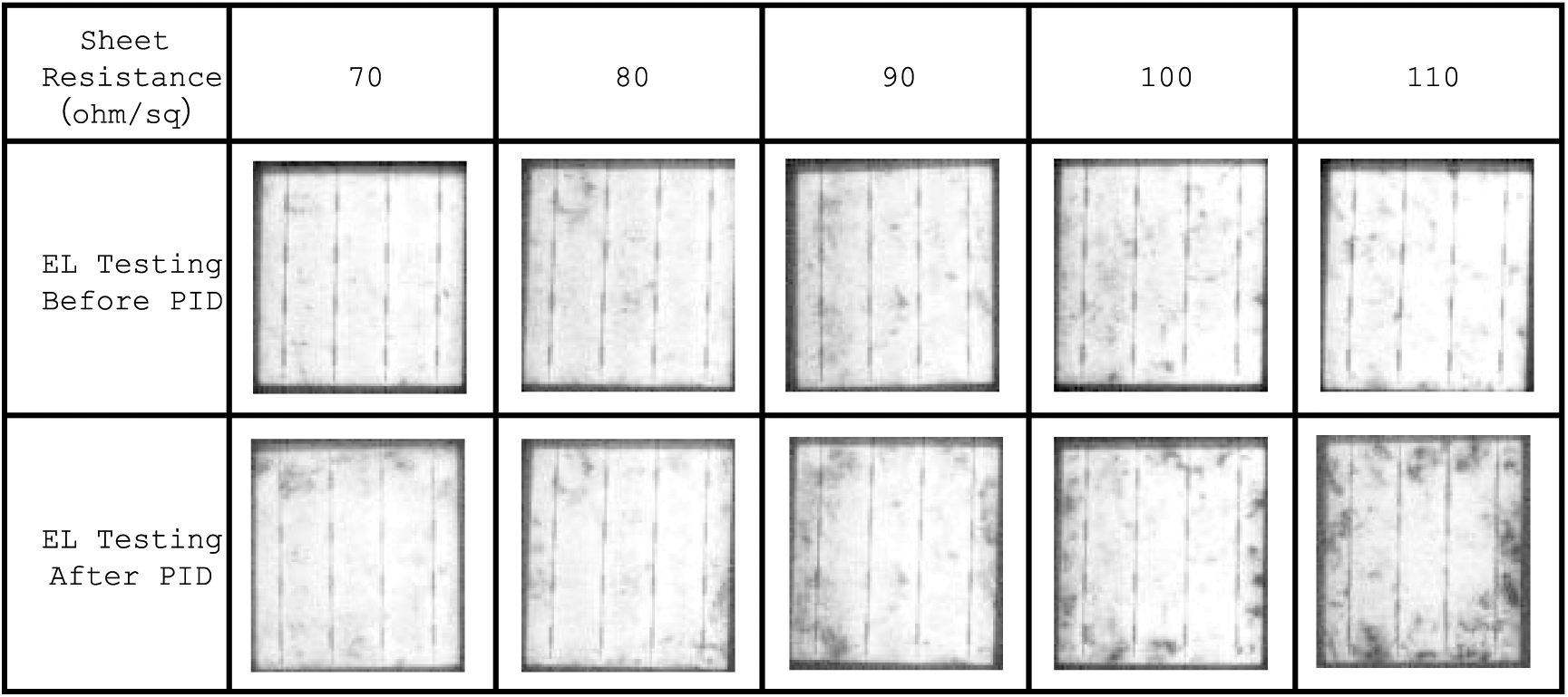
EL images of cells with different emitters before and after PID testing.
In order to further verify the reliability of PID testing results, a PIDcon tester was used to test the PID of cells. The cells were placed on an aluminum plate at constant temperature. Ethylene Vinyl Acetate (EVA) and glass were put on the surface of cells one by one as well. The testing probe touched the main grid line of the cells and a metal cover was placed on the surface of the glass to ensure the high voltage passed through the testing area. During the PIDcon testing, the Rsh change was calculated by testing the change of the current passing through the cells, and the cells with different sheet resistances of 600–900 ohm were chosen to ensure the comparison accuracy. Figure 7 shows the variation of Rsh with testing time. When Rsh is 110 ohm/sq, the relative value of Rsh decreases rapidly after PID testing for 2 h. The decrease of the Rsh value at the sheet resistances of 100 ohm/sq and 110 ohm/sq seems insignificant after PID testing for 2 h. When the sheet resistance increases from 70 ohm/sq to 90 ohm/sq, Rsh varies smoothly with the extension of testing time. When the testing time is 14 h, the relative value of Rsh at the sheet resistance of 90 ohm/sq begins to decrease rapidly and then becomes smooth gradually. After PID testing for 18 h, the rate of decrease of the Rsh value at the sheet resistance of 80 ohm/sq exceeds that at 70 ohm/sq, and then becomes smooth gradually. To sum up, with the increase of sheet resistance, the relative value of Rsh after PID testing decreases, the probability of electrical leakage increases, and the PID phenomenon is aggravated. This further verifies the testing results of the modules. Figure 8 shows the schematic of the PID mechanism at the P–N junction of crystalline solar cells. As can be seen, the doping concentration of phosphorus atoms decreases gradually with increasing sheet resistance, and the ability of gettering metallic ions in the silicon body decreases. At the same time, the passivation result of dislocation defects can increase the electric leakage channel, thus inducing the PID phenomenon.
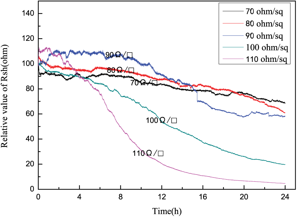
Variation curves of parallel resistance with testing time.
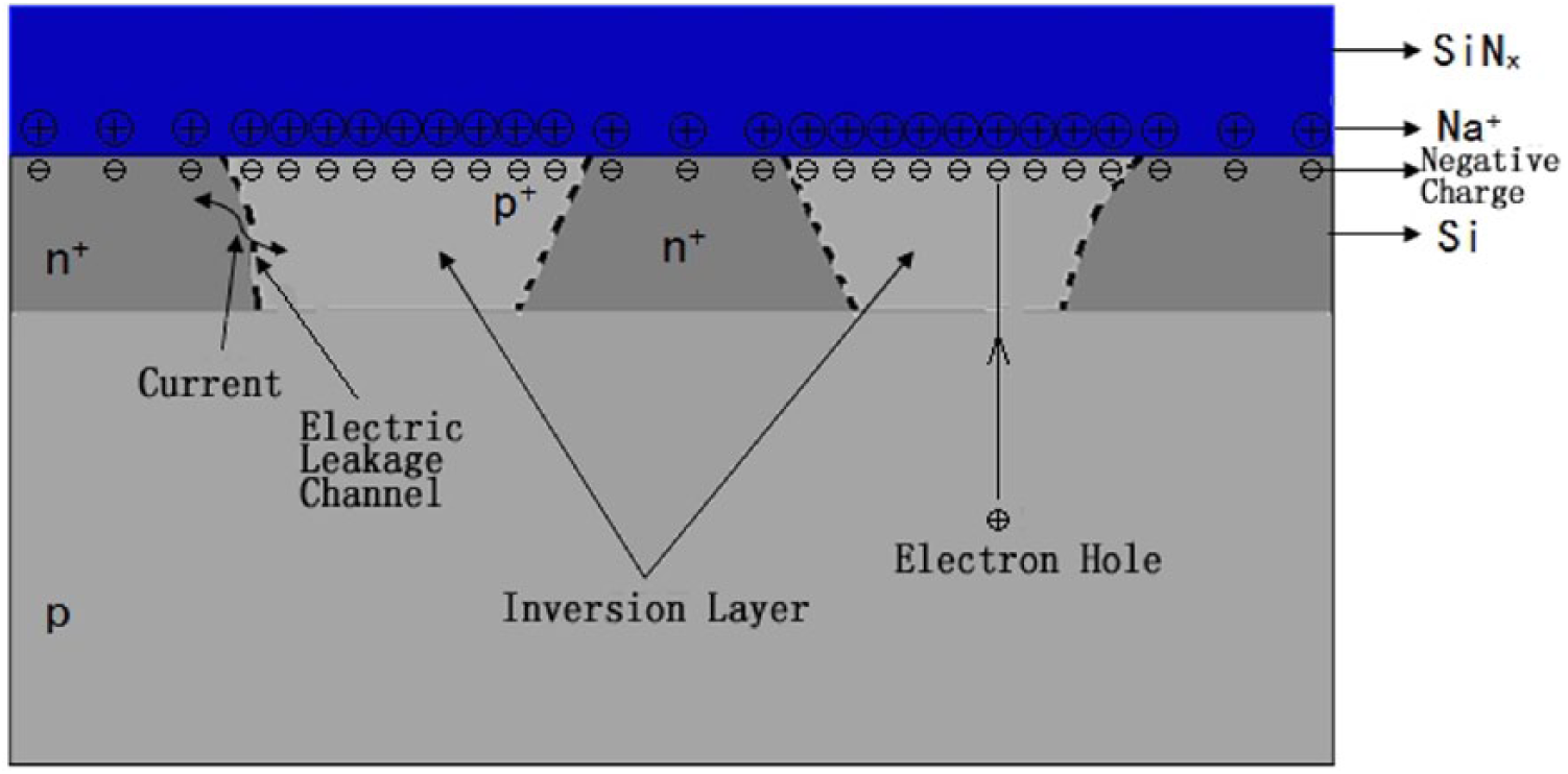
Schematic of PID mechanism at the P–N junction of crystalline solar cells.
Conclusions
The mechanism of PID in the process of cell diffusion technology was discussed in this paper. Lots of positive charges assembled at the interface of SiNx/Si, and then negative charges were induced at the interface because of the negative bias effect. These negative charges assembled on the surface of the silicon and attracted electron holes, which caused the increase of electron holes on the surface of the silicon. When the electron hole concentration was higher than the charge concentration, an inversion layer was generated on the surface of the emitter, and part of the P–N junction disappeared. The generated shunt could induce the PID phenomenon because of the electrical leakage in some areas. Especially when the sheet resistance was high, the doping concentration and the depth of P–N junction were non-uniform, and the inversion layer appeared extremely easily at a lower depth of the P–N junction. When the doping concentration was higher, the sheet resistance of the P–N junction was lower and the junction depth was higher. The P–N junction at a higher depth was less affected by negative charges, which were unable to cause greater electron hole concentration than the charge concentration. In this case, it was not easy to induce the inversion phenomenon of the P–N junction, thus decreasing the degree of PID. Therefore, it is more difficult to induce the PID phenomenon at lower sheet resistance and higher junction depth.
Footnotes
Declaration of Conflicting Interests
The author(s) declared no potential conflicts of interest with respect to the research, authorship, and/or publication of this article.
Funding
The author(s) disclosed receipt of the following financial support for the research, authorship, and/or publication of this article: This work was supported by the National Key New Products Foundation (Grant No. 2014GR364020) and Jiangsu Planned Projects for Postdoctoral Research Funds (1701072B) with the industrial partner CECEP Solar Energy Technology (Zhenjiang) Co., Ltd.