
Abstract
This article describes the local deposition, or micropatterning, of silica nanoparticles (NPs) using an electrospray method with a stencil mask. The proposed technique can be carried out in a single step at room temperature and atmospheric pressure under dry conditions, allowing it to be used with water- or vacuum-sensitive materials, and leading to cost reductions and high throughput. An evaluation of the patterning accuracy using a 20 µm thick mask showed that for patterns with line widths greater than 50 µm, the pattern was reproduced with an accuracy greater than 95%. When silver NPs were preferably deposited on the silica NPs using a modified silver mirror reaction, they were found to exhibit strong surface-enhanced Raman scattering effects. The proposed process is readily applicable to the development of high-performance micro total analysis systems.
Introduction
Silica nanoparticles (NPs) are of extreme interest for a wide range of applications, including surface modification, catalysts, fluorescent chemosensors, battery separators, and surface-enhanced Raman scattering (SERS)–based sensors.1–13 Silica NPs possess the advantages of a high specific surface area, excellent optical properties, hydrophilicity, and high chemical and physical stability. For example, Yamazaki et al. 2 demonstrated that the wettability of a hydrophobic polymer gate dielectric by a soluble organic semiconductor was drastically improved by depositing silica NPs on the dielectric. Suzuki et al. 6 developed mesoporous silica spheres with catalytic sites in the core potion and adsorption sites in the shell portion. The acid catalytic activity of the synthesized silica particles was found to be strongly augmented. Yang et al. 11 demonstrated a SERS-based sensor using a substrate coated with silica spheres with silver shells.
To make the best use of such applications, it is crucial to develop methods for micropatterning, or local deposition, of silica NPs. 14 One such method is self-assembly patterning,15–17 which is based on modification of the wettability of a substrate. Although this method is simple, it is a wet process, and the resulting pattern can often be affected by surface tension and capillary flow during the drying stage. 18 Dry processes have also been developed19–22 and include methods based on electron-beam lithography 23 and interferometric lithography, 24 which offer high resolution and thickness uniformity. However, these dry processes require many fabrication steps, which leads to low throughput and high cost.
In this study, we propose a single-step dry process for micropatterning silica NPs using electrospray deposition (ESD) and a stencil mask. The mask can be used repeatedly and can be of the type widely employed for micropatterning during physical and chemical vapor deposition.25–28 Since the proposed process involves a single step and can be conducted under dry conditions at room temperature and atmospheric pressure, it is expected to lead to cost reductions and high throughput. In addition, it can be used with water- or vacuum-sensitive materials.
Recently, SERS-based sensing has been combined with micro total analysis systems (MicroTAS) to achieve highly sensitive detection of extremely small volumes of biological and chemical analytes on a chip. 29 In this sensing technique, the active SERS region must be patterned at a specific site in the microchannel. In the present study, the feasibility of using the proposed single-step method in such a device is assessed by analyzing the pattern accuracy of the deposited silica NPs.
Materials and Methods
Reagents and Materials
Tetraethyl orthosilicate (TEOS), ethanol (99.5%), and hydrochloric acid (HCl; 1.0 M), used for ESD of silica NPs, were purchased from Wako Chemicals Co. (Richmond, VA). For the deposition of silver NPs, silver nitrate (0.3 M), ammonia (1.5 M), and hydrazine were purchased from Wako Chemicals Co., and Disperbyk-102 was purchased from BYK Japan Co. (Osaka, Japan).
The stencil mask was made of nickel and was manufactured by Tokyo Process Service Co. Ltd. Figure 1 shows the mask pattern, which includes linear slits with line widths of 30, 40, 50, 75, and 100 µm, and lettering patterns with line widths of 50, 100, 200, and 500 µm. The thickness of the mask was 20 µm.
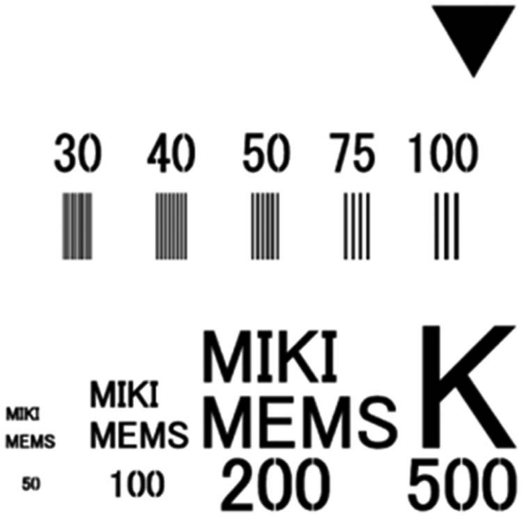
Design of nickel stencil mask.
ESD of Silica NPs
To prepare the precursor TEOS sol, a mixture of TEOS (9.0 mL), deionized water (4.6 mL), ethanol (14.5 mL), and HCl (1.0 mL) was stirred at room temperature in a Teflon container for 5 min. The mixture was then heated at 70 °C for 15 h, until the TEOS sol had a viscosity of 7 mPa·s.
Figure 2 shows a schematic view of the electrospraying system, which consists of a glass syringe, a syringe pump, an electrical source, and a silicon substrate with a stencil mask. The glass syringe had an 8 mm diameter nozzle and was filled with the prepared TEOS sol. During this procedure, bubbles trapped inside the syringe were carefully removed. The syringe was placed horizontally at a height of 120 mm from the ground. A 20 mm × 20 mm square silicon substrate with a thickness of 0.5 mm was placed 40 mm away from the nozzle of the syringe. To micropattern the silica NPs, the silicon substrate was covered with the mask.
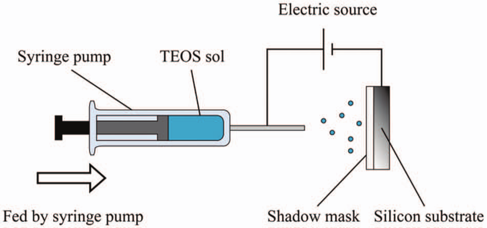
Schematic diagram of electrospray deposition method.
The electrospraying conditions were based on our previous work. 12 The viscosity of the TEOS sol was 7 mPa·s. A DC voltage of 6.2 kV was applied between the substrate and the nozzle. The feed rate of the sol in the syringe was 1.0 mL/h, and the total amount of fed sol was 0.01 mL.
Characterization of Deposited Silica NPs
The structure of the deposited silica NPs was observed using field emission scanning electron microscopy (FE-SEM; S-4700; Hitachi, Tokyo, Japan). The NPs were coated with a very thin layer of osmium by plasma sputtering (HPC-1S; Vacuum Device Inc.) to prevent charging. The width of individual lines in the NP pattern was measured using digital microscopy (VHX-600; Keyence, Osaka, Japan) and image-processing software (ImageJ; National Institutes of Health, Bethesda, MD). Images were first converted to eight-bit grayscale. An intensity histogram from a 300 × 300 pixel region containing no silica NPs area was then measured to determine the background level, which was set at the mean of the histogram plus three standard deviations (3σ). To determine the width of deposited lines, 10 intensity profiles across each line were measured per sample. The width of the deposited line was taken to be the distance between the leftmost and rightmost points of intersection between the intensity profile and the background level.
To determine the NP density distribution in the deposited pattern, the fraction of the area covered with silica NPs in SEM images was measured using ImageJ. For any given line, the NP density was evaluated in three different regions (left, middle, and right) to determine the density distribution across the width of the line. The left region began with the leftmost NP and extended 5 µm across the width of the line. Similarly, the right region began with the rightmost NP and extended 5 µm across the width of the line. The middle region was a 5 µm wide strip centered on the midpoint between the leftmost and rightmost NPs.
Deposition of Silver NPs
Silver NPs were deposited using a modified silver mirror reaction, in which dispersants were added to the solution.30,31 A silver NP solution was prepared by mixing 0.3 M silver nitrate (5.0 mL), 1.5 M ammonia (8.0 mL), deionized water (20 mL), and the dispersant Disperbyk-102 at 25 °C. A silicon substrate with deposited silica NPs and a flat glass plate (S9111; Matsunami Glass Ind. Ltd., Osaka, Japan) were exposed to oxygen plasma for 35 s and immersed into the silver NP solution. Then, 6.0 mL of hydrazine was added to the solution as a reducing agent. After 80 s, the substrate was removed from the solution, rinsed with deionized water, and dried using a nitrogen gas flow. The silver NPs are preferably deposited on the silica NPs.
SERS Experiment
To verify the usefulness of the substrate with deposited silica and silver NPs as a SERS sensor, Rhodamine 6 G (R6G; Wako Chemicals Co.) was used as an analyte. R6G was dissolved in ethanol and adjusted to a concentration of 100 µM, and 20 mL of the solution was dispersed on a substrate using a pipette. After the solution was dried fully, SERS measurements were conducted using a CCD Raman system (STR 300-3LCCD RAMAN; Seki Technotron Co., Tokyo, Japan). The measurement conditions were a wavelength of 532 nm, a lens magnification of 20 times, a spot diameter of 10 µm, and an integration time of 3 s. During Raman measurements on silver NPs on silica NPs, the spectra were obtained from the middle region of each patterned line.
Results and Discussion
Micropatterning of Silica NPs
Figure 3 shows FE-SEM images of silica NPs deposited on a silicon substrate through the stencil mask. The NP size ranged from 50 to 250 nm. Figure 4 shows optical micrographs of silica NPs deposited through the slits of the stencil mask. The scale bars in the figures are 100 µm. These images show that silica NPs could be successfully patterned on the silicon substrate using the proposed method. Figure 5 shows the ratio of the line widths in the silica NP pattern to those in the mask. For all line widths in the mask, the ratio was greater than 0.8 and was 0.95 when the line width was larger than 50 µm. The slight reduction in the line widths in the deposited pattern is thought to be related to an attractive electrostatic force between the mask and the flying NPs. It was previously reported that this type of reduction was the result of a focusing effect due to a repulsive force between positively charged flying NPs and those deposited on a nonconductive mask. 32 However, in the system used in the present study, the mask is expected to be negatively charged during silica NP deposition of silica because it is made from conductive nickel and in direct contact with the negatively charged substrate. The conductivity of the mask was kept after the deposition of the silica NPs. Another possible reason for the reduction is a shadowing effect by the side walls of the mask. In vapor deposition techniques, it is known that a width reduction occurs due to shadowing by a membrane with a nonzero thickness and the oblique incident angle of the evaporated material. 26 To consider this possibility, the NP density distribution in the deposited pattern was measured. Figure 6a shows an SEM image of a section of a deposited line of silica NPs; the three different regions used to measure the NP density are indicated by the broken lines. Figure 6b shows the fraction of the area covered with silica NPs in these three regions for different mask line widths. If side-wall shadowing is the main cause for the width reduction, the density at one edge of the line where shadowing is taking place should be lower than that in the middle region and at the other edge. However, Figure 6b shows that the density at both edges of the line decreased by about the same amount compared with that in the middle region. This result leads to the conclusion that an attractive electrostatic force due to the negatively charged mask is likely to be the main cause of the reduction in the line width and the NP density at the line edges in the deposited pattern by deflecting the NPs flying near the edge of a slit.
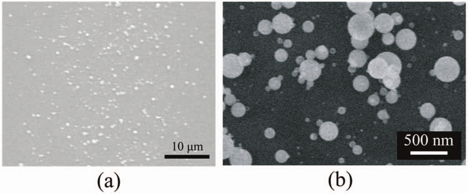
Field emission scanning electron microscopy images of deposited silica nanoparticles patterned on silicon substrate through 50 µm wide slit. (
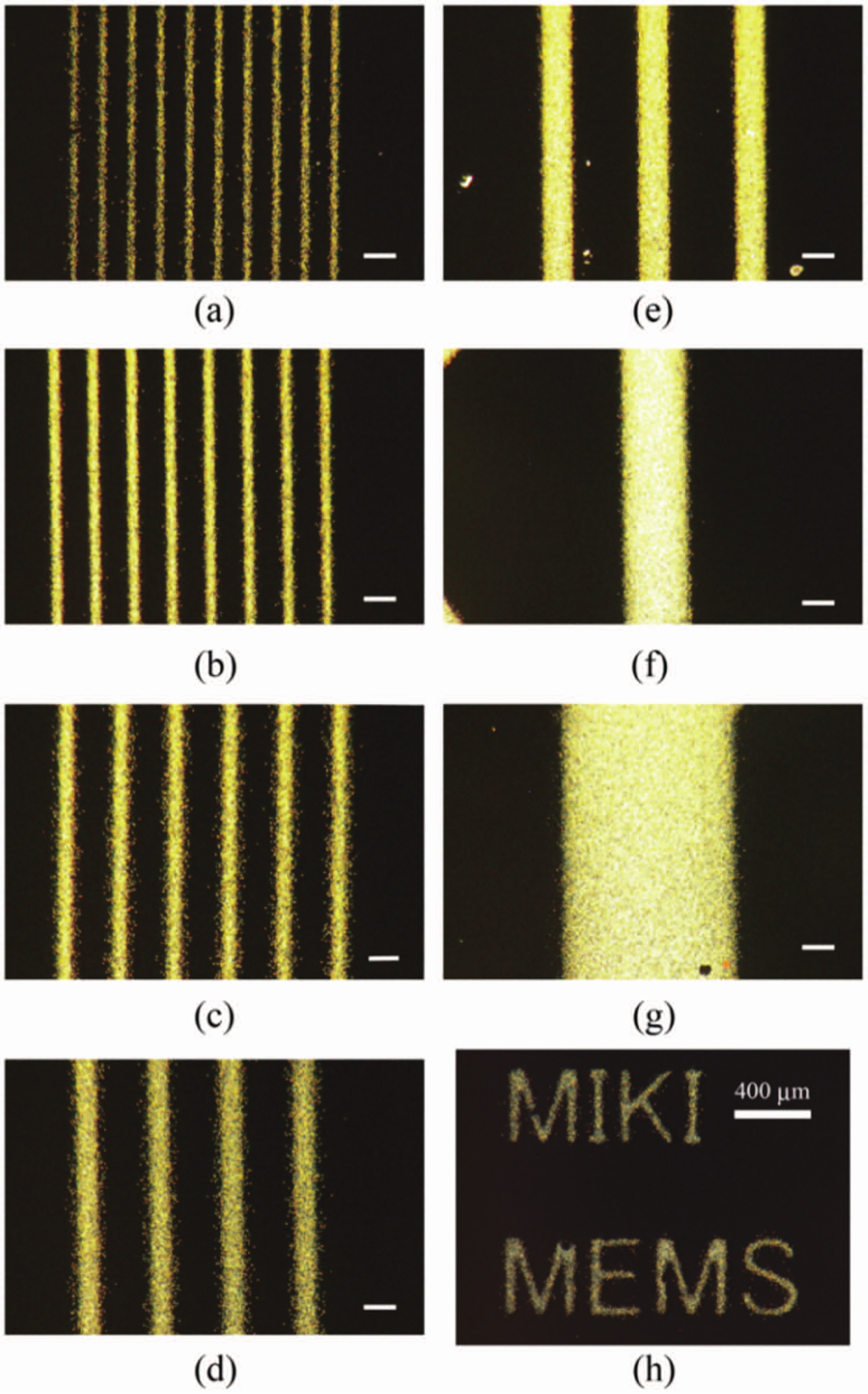
Optical micrographs of silica nanoparticles (NPs) micropatterned through linear slits with widths of (
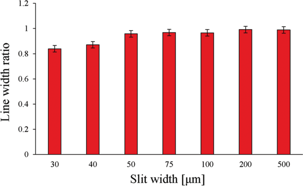
Ratio of line width in deposited pattern to that in mask as function of slit width.
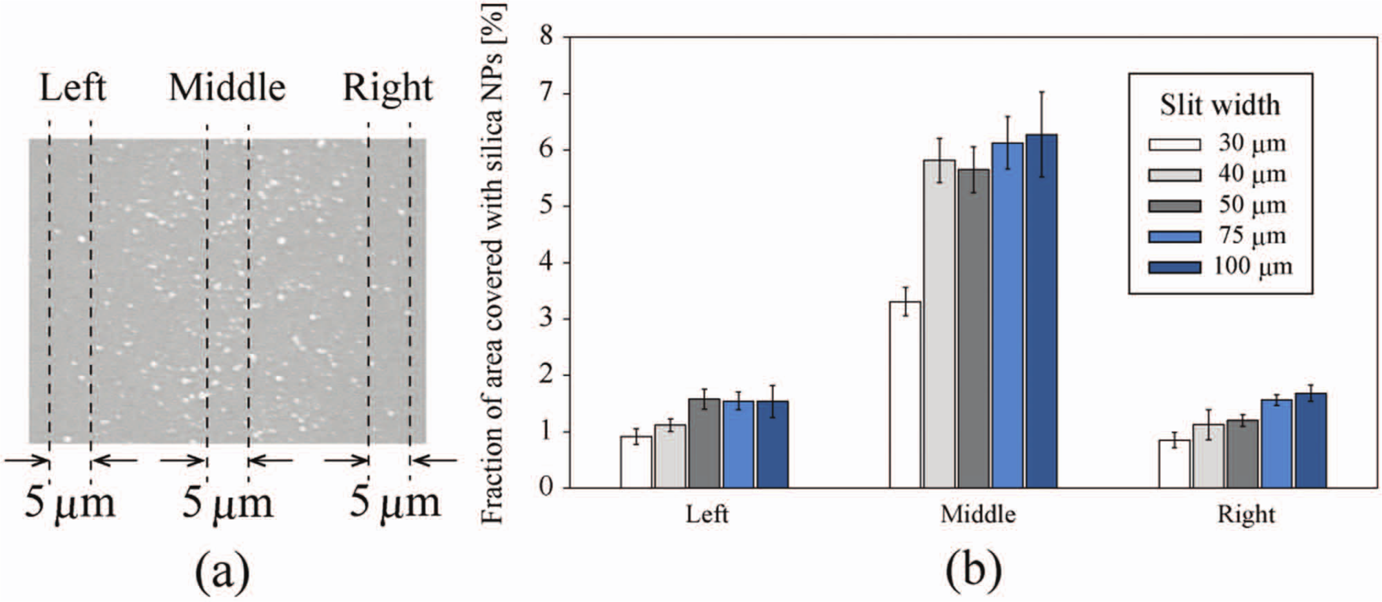
Nanoparticle (NP) density distribution across the width of deposited lines. (
SERS on Patterned Silica NPs Coated with Silver NPs
Figure 7 shows Raman spectra of R6G recorded detected using silver NPs on silica NPs, silver NPs on a flat glass plate, and a bare glass plate. It can be seen that for the silver/silica NP combination, the Raman scattering intensity is greatly enhanced compared with the other two cases. Clear bands are observed at 930, 1176, 1297, 1349, 1503, 1566, 1594, and 1649 cm−1, and these are characteristic of R6G.33,34 SERS is considered to have the optimum structure (i.e., highly sensitive to the local nano structure 30 ), and it was previously shown that silver NPs deposited on glass NPs from a 0.01 mL sol exhibited a SERS signal that was three times stronger than that from silver NPs deposited on a flat glass substrate. 12 This is consistent with the results of the present study, indicating that silica NPs micropatterned using a stencil mask can be also applied to SERS sensors.
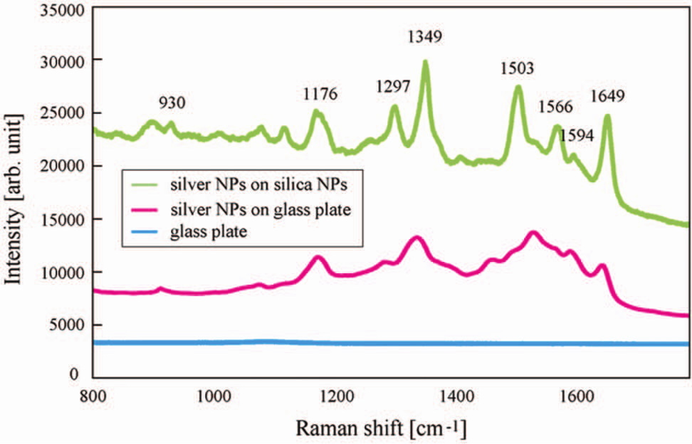
Raman scattering spectra of R6G on combined silica/silver nanoparticles (NPs), silver NPs on flat glass plate, and bare glass plate.
Thus, by combining the techniques of silica NP patterning and silver NP coating, sensitive SERS detection sites can be created, and these can be integrated with microfluidic components to develop MicroTAS devices that are capable of both sample preparation and analysis. 34
Conclusion
A micropatterning technique was proposed that involves electrospraying silica NPs onto a substrate through a stencil mask. This process can be conducted at room temperature and atmospheric pressure under dry conditions and requires only a single step. This makes it a potentially low-cost, high-throughput process that can be used with water- or vacuum-sensitive materials. The patterning accuracy was experimentally verified using a 20 µm thick stencil mask made of nickel, through which silica NPs were successfully micropatterned on a silicon substrate. The line widths in the NP pattern were found to be slightly smaller than those in the mask, and the NP density was lower near the edges of patterned lines than in their center. This is thought to be due to the influence of an attractive electrostatic attractive force between the NPs and the mask. It was shown that the patterned silica NPs acted as a substrate for preferential deposition of silver NPs, and the resulting structure exhibited strong SERS effects. Thus, the proposed micropatterning process is readily applicable to high-performance MicroTAS devices.
Footnotes
Declaration of Conflicting Interests
The authors declared no potential conflicts of interest with respect to the research, authorship, and/or publication of this article.
Funding
The authors disclosed receipt of the following financial support for the research, authorship, and/or publication of this article: This work was supported by a Grant-in-Aid for Scientific Research (S) (2122606).