
Abstract
Perylene 3,4,9,10-tetra carboxylic dianhydride (PTCDA) thin films find a lot of optoelectronic applications. In this work, thin films of PTCDA were deposited using vacuum evaporation technique onto clean glass substrates and the variation in conductivity, optical bandgap and percentage transmission due to iodine doping for different time intervals are discussed. To study the doping effects on devices, organic solar cells based on cobalt phthalocyanine (CoPc)/PTCDA as active layers on indium tin oxide–coated glass substrates were fabricated and characterized to evaluate the solar cell parameters. It was found that doping with iodine considerably increases the power conversion efficiency of the solar cells.
Introduction
Organic semiconductors are expected to play a vital role in both industry and research in the coming years. Perylene derivatives are commercially available as red pigments with electrical and optical properties that allow them to be compared with conventional inorganic wide bandgap semiconductors. 1,2 Recently, a lot of research were done on the study of the archetype molecular compound Perylene 3,4,9,10 tetracarboxylic dianhydride (PTCDA). The primary motivation for focusing on PTCDA is its promising optical and electronic properties. 3,4 The PTCDA films find optoelectronic applications and serve as a model substance for the investigation of thin organic film and possible future devices. 5–7 Electrical property studies of thin films are a subject of current interest, as they may lead to useful electronic devices. In the present work, thin films of PTCDA were deposited using vacuum evaporation technique and the doping effects of iodine (I2) on the electrical conductivity and optical bandgap of the PTCDA films were evaluated. Variation in percentage transmission due to doping is also reported. Similarly, transition metal-based phthalocyanines like cobalt phthalocyanine (CoPc) have attracted attention in the areas of fuel cells, gas sensors, biosensors, and electronic devices like driver transistors and solar cells. 8–11 For studying the doping effects on devices, CoPc active layers were used in the heterojunction.
Materials and Methods
Spectrographically pure materials were purchased from Sigma (Aldrich) and used without further purification. Thin films of PTCDA were deposited by vacuum evaporation technique using a Hind Hivac vacuum coating unit in a molybdenum boat. Glass substrates were first cleaned using an ultrasonic cleaner and then with acetone. Films were deposited at the rate of 10 Å/s in a vacuum of about 2 × 10⁻⁶ Torr. Thicknesses of the films were measured using a digital thickness monitor. Usually, doping of thin films are done by co-evaporation or by subsequent evaporation on the top of the organic layer. 12–14 In the present work, vacuum-evaporated PTCDA thin films were doped with I2 using two methods: an evaporation process (say, process 1) and a dip process (process 2). In the evaporation process, I2 crystals were allowed to evaporate in a vacuum desiccator and the daily variation in electrical conductivity is measured using a Keithley (USA, a Tektronix company) 2400 model source meter. In the dip process, PTCDA thin films were doped by immersing into a solution of I2 diluted in acetonitrile (5 mg/300 mL) for different time durations (<1 h). Then the room-temperature dark conductivity was measured and the optical properties were studied.
For the deposition of CoPc thin films, a vacuum evaporation technique was employed and then the films were doped with I2. Then the thin films of PTCDA were deposited onto these CoPc thin films using vacuum evaporation technique and were doped with I2. We studied the doping effects of I2 on the electrical and device properties of CoPc/PTCDA solar cells. Structure of the device fabricated was Al/CoPc-I2/ PTCDA-I2/PEDOT-PSS (polyethylene dioxythiophene–poly styrene sulfonic acid)/indium tin oxide (ITO)/glass.
Results and Discussion
Conductivity studies on doped and undoped PTCDA thin films showed that the conductivity increases from 7.6 × 10⁻⁵ Ω−1 m−1 to a maximum of 2.8 × 10⁻³ Ω−1 m−1 on doping. In earlier reports, increase in conductivity due to I2 doping was explained as due to the structural variation in the PTCDA thin films during doping. 15,16 In the present work, doping effects are more and fast for the dip process, as expected.
For optical studies on doped and undoped PTCDA thin films, optical spectra were taken for samples with %T versus wavelength λ. Transmission spectra for undoped and doped (process 1) PTCDA thin films are shown in Figure 1. The spectra demonstrated an interference pattern with a sharp fall at the band edge, indicating a semiconductor behavior with a good crystallinity. For the undoped PTCDA thin films, a complete absorption was observed in the visible range. For the doped PTCDA thin films, %T showed a slight increase in the visible range, indicating that the doping of PTCDA films with I2 has an observable effect on the transmission properties. This increase in %T for the doped PTCDA thin films was attributed to the scattering of light in the dopant atoms, which was absent in the undoped films. Transmission spectrum also reveals that due to doping, PTCDA thin films were having a strong absorption in the near-infrared region.

%T versus λ for the undoped and doped (process 1 for 1 day) PTCDA thin films. PTCDA, perylene 3,4,9,10-tetra carboxylic dianhydride.
Absorption coefficient α is related to the photon energy hν by,

where Eg is the optical bandgap.
For the allowed transitions, (αhν) 2 is plotted against hν, from which the extrapolation of the linear portion to α = 0 near the absorption edge gives the bandgap energy. For the undoped PTCDA film, the optical bandgap obtained from the graph was about 2.96 eV as shown in Figure 2A. Narrowing of the bandgap was also observed for the doped PTCDA samples. Similarly, for the dip process doped PTCDA thin films, bandgap decreased to 2.75 eV as shown in Figure 2B. Red shift is also observed for these samples. Optical and electrical parameters of PTCDA thin films are tabulated in Table 1. Here the dopant establishes a highly doped surface region on top of the PTCDA layer and the excess dopant diffuses into the film as per the X-ray photoelectron spectroscopy and Fourier transform infrared studies in an earlier report. 13 Hence a drastic variation in the optical and the electrical parameters of PTCDA thin films was observed due to doping. A detailed study on the structural changes of these films due to doping is necessary for tuning the electrical and optical properties of device applications.

(αhν) 2 versus hν plot for (A) undoped PTCDA thin film (B) PTCDA-I2 thin film (dip process for 30 min). PTCDA, perylene 3,4,9,10-tetra carboxylic dianhydride; I2, iodine.
Optical and Electrical Parameters of Undoped and Doped PTCDA Thin Films.
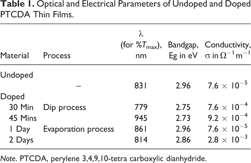
Note. PTCDA, perylene 3,4,9,10-tetra carboxylic dianhydride.
Next, to evaluate the doping effects of I2 on PTCDA devices, CoPc was selected as the active layer for PTCDA solar cells. CoPc films were annealed in air and then doped with I2. Similarly, PTCDA layer was also doped after its deposition onto the CoPc layer. Doping of PTCDA layer with I2 was done for different timings such as 4 h, 20 h, 24 h, and 48 h. Then Ca layer was deposited followed by the Al electrode contact layer deposition and subsequently the devices were characterized. Al was deposited from a tungsten basket and Ca was deposited using electron beam evaporation technique. Light characteristics of a CoPc-I2/PTCDA organic solar cell are shown in Figure 3. It was found that the solar cell efficiency increases due to doping as shown in Table 2. It was seen that series resistance also showed a hike with I2 doping for the devices. Maximum efficiency of 0.01% is obtained for the nonannealed devices with CoPc (doped for 20 h)/PTCDA and CoPc/PTCDA (doped for 20 h) active layers as shown in Table 2. When the doping time was increased for more than 20 h for the PTCDA layer, the efficiency was found to decrease. So, it can be concluded that the doping of the CoPc or PTCDA can drastically modify the properties of the organic devices. 17,18 Devices fabricated with an annealed and doped layers may improve the overall performance of the devices suitable for various applications.

Light characteristics of a nonannealed CoPc-I2/PTCDA organic solar cell. CoPc, cobalt phthalocyanine; I2, iodine; PTCDA, perylene 3, 4, 9, 10-tetra carboxylic dianhydride.
Device Parameters of CoPc-I2/ PTCDA-I2 Solar Cells.

Note. CoPc, cobalt phthalocyanine; I2, iodine; PTCDA, perylene 3,4,9,10-tetra carboxylic dianhydride.
Conclusions
Thin films of PTCDA were deposited using the thermal evaporation process under high vacuum onto the cleaned glass substrates. These films were then doped with I2 by an evaporation process and a dip process. It was found that the conductivity increases on I2 doping. Conductivity increases to a maximum value for a highly doped sample. It is also found that the doping effects on the properties are more evident and fast for the dip process in both thin films and the devices.
Footnotes
Acknowledgments
Financial support by Visvesvaraya Technological University (VTU), Belgaum, Karnataka, India, through a grant is gratefully acknowledged. Support by Vision Group on Science and Technology (VGST), Department of Information Technology, Biotechnology & Science and Technology, Government of Karnataka, India, is also acknowledged.
Declaration of Conflicting Interests
The author(s) declared no potential conflicts of interest with respect to the research, authorship, and/or publication of this article.
Funding
The author(s) disclosed receipt of the following financial support for the research, authorship, and/or publication of this article: This project was funded by Visvesvaraya Technological University (VTU), Belgaum, Karnataka, India, through a research grant.