
Abstract
In this study, we evaluated a nanoscale random rubbed structure (nRRS) used as a scattering layer in organic light-emitting diodes (OLEDs) through an innovative manufacturing method. The rubbing technique, which is conventionally utilized only for liquid crystal alignment, is a manufacturing process with excellent merit in that it can form nanoscale random corrugation in a large area without vacuum equipment even at room temperature, and it is simple and inexpensive. The optimized nRRS, fabricated via rubbing, exhibited a high transmittance of 97.8% and haze of 17.8%, making it suitable as a scattering layer for OLEDs. Owing to its random nature, the scattering effect occurred effectively by rearranging the waveguided light inside the glass substrate. The OLED combined with the optimized nRRS showed a 25.4% improvement in the external quantum efficiency. Additionally, the spectral distortion according to the viewing angle was alleviated, which was confirmed by the negligible difference in the International Commission on Illumination 1931 color space coordinates (∆(x, y) = (0.01, 0.013)). The optical performance of the nRRS–OLED was predicted through a finite-difference time-domain simulation and verified by showing results consistent with those of the fabricated device. This research is expected to be widely applied in many optical devices because it is possible to form a random corrugation on the outside of the device without the difficulty of simply fabricating a beneficial optical structure.
Keywords
Introduction
Organic light-emitting diodes (OLEDs) are regarded as next-generation displays owing to their excellent color expression, self-emitting characteristics, high-speed operation, and applicability to deformable displays.1–4 Owing to the development of light-emitting materials such as phosphorescent materials and thermally activated delayed fluorescence materials, OLEDs have theoretically achieved an internal quantum efficiency of nearly 100%.5–7 Nevertheless, unless special techniques are applied, the external quantum efficiency of OLEDs, which is the product of the internal quantum efficiency and outcoupling efficiency, is only about 20%. 8 The limitation of the external quantum efficiency is due to the total internal reflection in the substrate and anode/organic layer and the light propagation loss at the metal-organic interface. The total internal reflection loss in the substrate is referred to as the substrate mode and is caused by the difference between the refractive index of air (n = 1.0) and the glass substrate (n = 1.5).9,10 Similarly, the waveguide mode occurs because of the refractive index mismatch between the glass substrate and indium tin oxide (ITO) (n = 1.9) or indium zinc oxide (IZO) (n = 2.0), which are mainly used as anodes, and the organic layers (n = 1.7).11,12 In addition, there is another lossy mode called the surface plasmon polaritons mode that propagates along the organic-metal surface due to interactions between electromagnetic waves and surface plasmons.13,14 To extract the waveguide mode and surface plasmon polariton mode, it is necessary to apply a deformation inside the device. However, because the substrate mode is generated at the interface with air, the extraction of the substrate loss is possible without changing the internal structure of the device.
Various techniques have been adopted to utilize the light trapped inside a glass substrate, including external scattering layers,15–19 microlens arrays,20–22 and surface texturing .10,23 Most of these techniques focus on converting the substrate loss into emission to air by modifying the light path via scattering. Additionally, there are approaches such as the periodic photonic crystal structure,12,24,25 random corrugation,26–29 and grid patterning30,31 that extract confined light by inserting a light extraction structure inside the device; however, these structures may cause spectral distortion according to the viewing angle or adversely affect the inner multilayer boundaries, thereby impairing electrical characteristics.32–34 Furthermore, to fabricate such a light extraction structure, it is necessary to utilize expensive equipment and complicated processes, such as various lithography techniques, plasma etching, and thermal dewetting. Most processes require vacuum chambers and the manufacturing of large OLEDs is limited.35–39
In our previous work, 40 we demonstrated an internal scattering layer using a nanoscale random rubbed structure (nRRS) to improve OLED performance using an SU-8 polymer via the rubbing technique. The rubbing technique is commonly used to anchor nematic liquid crystals in a desired orientation.41,42 This manufacturing approach has excellent advantages, such as the capability of large-scale applications, processability at room temperature and normal pressure conditions, and is a simple and low-cost method. The nRRS-inserted OLEDs exhibited enhanced performance owing to the light scattering effect. However, to increase the scattering effect, it was necessary to increase the size of the structure. When the nRRS was inserted inside the device, there was a roughness limit on the structure for stable electrical properties. When the height of the nRRS exceeded 100 nm, the electric field intensity was concentrated on the excessively steep structure, resulting in nonuniform current emission characteristics. Moreover, because of the relatively thick SU-8 polymer and IZO anode, all the nRRSs exhibited an extremely low haze, which was within 5%.
In this study, we further evaluated nRRS as an external light-extraction structure to enhance light-path scattering and improve the performance of OLEDs (Figure 1). By increasing the number of rubbings, it was possible to form a higher structure than when the nRRS was inserted inside the device, and it was also confirmed that the scattering effect was increased. The optimized nRRS showed a haze of 18%, and when it was combined with an OLED, an external quantum efficiency improvement of 25.4% compared with the reference device occurred. Because of its random nature, the spectral distortion characteristics according to the viewing angle were diminished, and this was verified through the minimum International Commission on Illumination (CIE) 1931 color space coordinate shift. The optical effects of the nRRS were analyzed using finite-difference time-domain (FDTD) numerical calculations. Schematic mechanism of external light scattering structure. Due to a slight refractive index mismatch between the glass substrate (n = 1.53) and the nRRS (n = 1.59), minor refraction occurs at the nRRS-glass interface.
Experiments
nRRS fabrication
A schematic of the fabrication process is shown in Figure 2. The SU-8 polymer (SU-8 2002, MicroChem.) was used to form the external scattering layer. The SU-8 polymer was spin-coated for 30 s at 3000 rpm onto an ITO-coated glass substrate on the glass side to form a uniform layer of 1.2 μm. Subsequently, the samples were annealed at a temperature of 70°C for 90 s on a hot plate for soft baking. After soft-baking, the rubbing fabric (HY-5318, Hyperflex) with a pile density of 53,000 EA/cm2 (Supplementary Figure S4) was buffed above the SU-8 polymer surface in a single direction with the force of 5.560 N (0.567 kgf), creating nanoscale corrugation on a large-area scale (100×100 mm). Pile density refers to the number of pile filaments per area of 1 cm2. Since the fabricated nanosized grooves were randomly distributed and suitable for visible light path redistribution, we named it nanoscale random rubbed structure. Ultraviolet light with a wavelength range of 350–400 nm was irradiated with an energy of 130 mJ/cm2 to harden the nRRS. All processes were carried out at room temperature (25°C) in the air atmosphere. Fabrication process of nRRS device.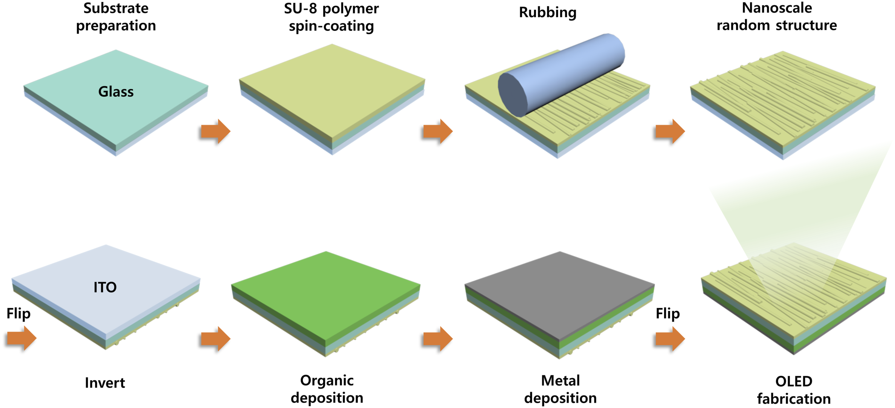
OLED fabrication
Prior to the process, an ITO-coated glass substrate (100 × 100 mm, 11.6 Ω/sq.) was cleaned by sonication in acetone, methanol, and deionized water, sequentially. After fabricating the nRRS on the glass surface, the substrate was diced to a sample size of 25 × 25 mm, optimized for the OLED manufacturing process. Subsequently, the sample was flipped over, and the ITO surface was treated using ultraviolet-ozone for 160 s, followed by oxygen plasma exposure for 160 s at 80 W power for work function adjustment. A green fluorescent OLED was deposited using a thermal evaporator system (Korea Vacuum Tech.) under high vacuum (∼10−7 Torr) conditions. The green OLED was constructed as follows: 60 nm of N,N-di(1-naphthyl)-N,N-diphenyl-(1,1-biphenyl)-4,4-diamine (NPB) as the hole transport layer, 80 nm of tris(8-hydroxyquinolianto)-aluminum (Alq3) as the light-emitting layer and the electron transport layer, 1 nm of lithium fluoride (LiF) as the electron injection layer, and 100 nm aluminum (Al) as the cathode.
Nanophotonic analysis
The optical results of the nRRS device were analyzed using the FDTD software (ANSYS, Inc.) to predict the emission properties. In the FDTD, the structure is divided into mesh units, and the strength of the electromagnetic field is calculated at the interface. The simulated model reflected the thickness and refractive indices of the multi-layered real device structure, and the refractive indices of each layer were measured using a thin film analyzer (F-20, Filmetrics, Inc.). After depositing the materials constituting the OLED on a silicon wafer to a thickness of 100 nm, the reflected signal is measured through a thin film analyzer to derive optical constants (refractive index and extinction coefficient) as a function of the wavelength (Supplementary Figure S1 and S2). The structure of the simulated OLED and the refractive indices at 520 nm wavelength (n520) were as follows: SU-8 (n520 = 1.59), glass (n520 = 1.53), ITO (n520 = 2.06), NPB (n520 = 1.81), Alq3 (n520 = 1.72), and Al (n520 = 0.84). The refractive index of SU-8 was measured after soft-baking and ultraviolet light curing. The simulation domain of the metal cathode was set as the metal and the other sides were set as perfectly matched layers. Three dipoles with different polarizations (x-, y-, and z-polarizations) were placed in the middle of the emitting layer. The light enhancement factor of the nRRS‒OLEDs compared to that of the reference device was calculated as the ratio of the electrical field intensity integration measured by a farfield monitor.
Measurement
The electroluminescence (EL) characteristics were measured in the normal direction and at different viewing angles using a spectroradiometer (PR-670, Photo Research) in a black box. The current-voltage characteristics were measured using a high-voltage source unit (Model 237, Keithley Instruments). Surface images of the nRRS were obtained through atomic force microscopy (AFM, XE-100, Park Systems), and the transmittance was measured using an ultraviolet‒visible near-infrared (NIR) spectrometer (Cary 5000, Agilent Technologies). Total transmittance was measured by the amount of light transmitted from all angles using the integrating sphere, and specular transmittance was measured by the amount of light transmitted only in the normal direction in the range of ±5° (Supplementary Figure S7). Haze is expressed as the ratio of diffused transmittance and total transmittance, and represents the degree of scattering due to surface roughness. Diffused transmittance can be derived as the difference between total transmittance and specular transmittance.
Results and Discussion
FDTD simulation
An FDTD simulation was performed to analyze the improvement in the light extraction efficiency according to the scattering effect of the nRRS. Four types of OLEDs were evaluated: the conventional bottom-emitting OLED (reference), SU-8 coated OLED without rubbing (planar), nRRS–OLED with a maximum height of 100 nm (H100), and nRRS‒OLED with a maximum height of 200 nm (H200). The simulation models of the different OLEDs are shown in Figure 3. To mimic the random nature of the nRRS, the structure was embodied by the array of the trapezoid-shaped SU-8 with various heights and tooth angles. To verify the trend of the scattering effect according to the difference in the roughness of the nRRS, nRRS‒OLEDs were simulated for two cases, H100 and H200, with different heights. The height of each nRRS was simulated as follows: the H100 device was varied from 50 to 100 nm, whereas the H200 device was varied from 100 to 200 nm. The tooth angle was varied from 45° to 80° for both devices. To visually verify the scattering effect according to the nRRS, the light intensity distribution was simulated with an electric field monitor for the cross-section of each device, and the electric field distribution in air for each angle was measured with a farfield monitor. FDTD simulation structure of the reference, planar, H100, and H200 devices.
The simulation results for each device are shown in Figure 4. Figures 4(a)–(d) show the electric field distributions induced by the emission dipoles of the reference, planar, H100, and H200 devices, respectively. Because the refractive indices of the glass and SU-8 polymer are relatively similar, the electric field distributions of the reference and planar devices are similar; however, as shown in Figure 4(c) and (d), where nRRS exists, the scattering effect can be clearly confirmed. The electric field distribution pattern in air was more pronounced in the H200 device with a larger nRRS height than in the H100 device. The scattering pattern by nRRS was demonstrated through an electric field monitor, and it can be expected that the haze of the nRRS–OLEDs is larger than that of the reference or planar devices. To verify the effect of nRRS on the improvement of the light efficiency, the farfield distribution results were derived and are shown in Figure 4(e)–(h). As in the previous results, the reference and planar devices showed a similar distribution, but in the H100 and H200 devices, the light intensity in the visible light wavelength range was scattered at various angles. Additionally, it can be observed that the intensity of the farfield is stronger in the H200 device, which has a larger nRRS. (a)–(d) Results of the electric field distribution of reference, planar, H100, and H200 devices, respectively. (e)–(h) Results of the farfield angular distribution of reference, planar, H100, and H200 devices, respectively.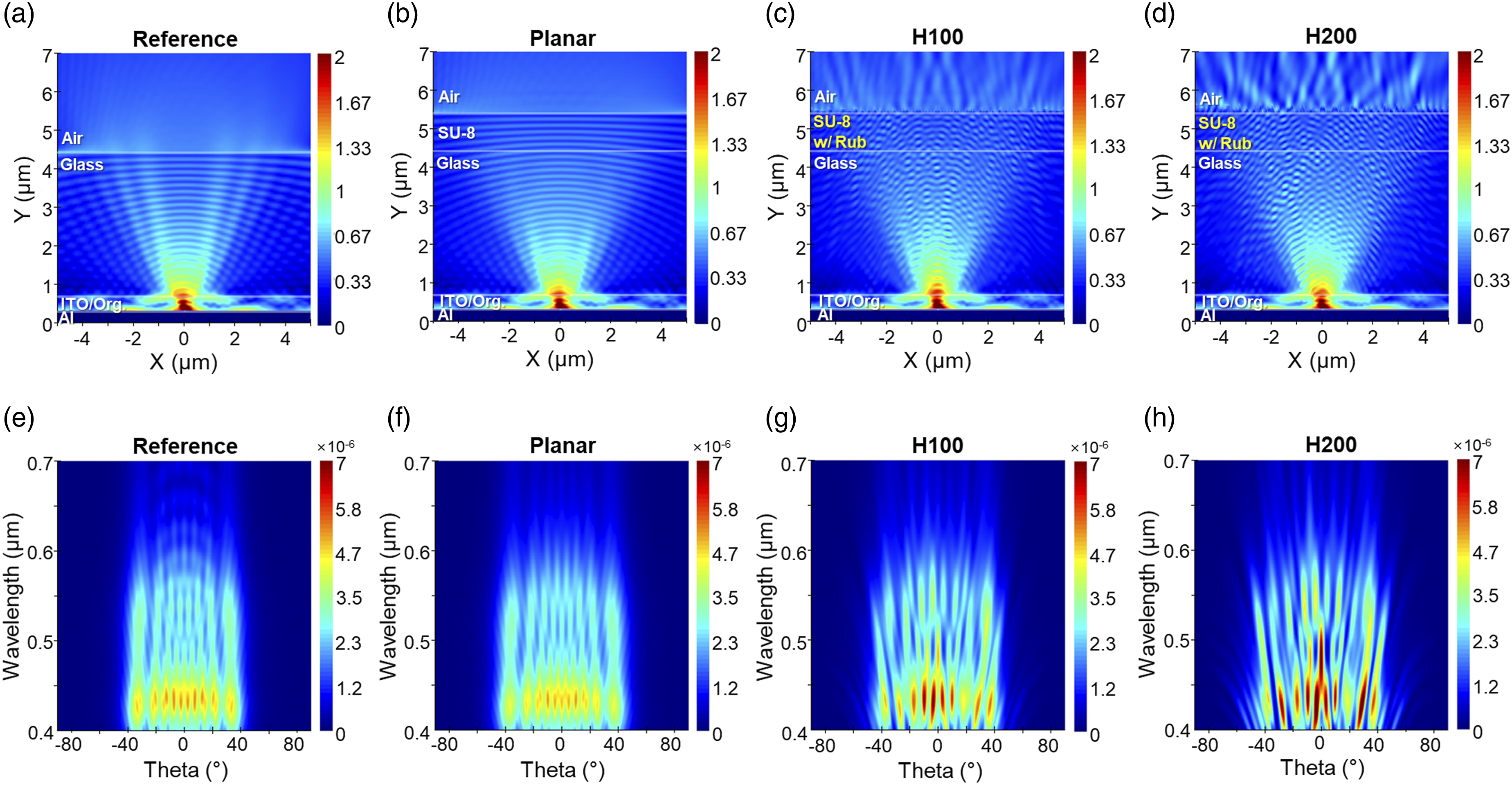
Figure 5 shows the light efficiency improvement of the three devices compared with the reference device by integrating the farfield distribution with respect to the angle. As the OLED is composed of multi-layer thin films, multiple interfaces are formed inside the device, which causes interference between lights. Therefore, due to the interference effect, reflectance and transmittance show an oscillating trend, which further affects the intensity of light according to the wavelength. In Figure 5, it can be seen that the light extraction enhancement factor oscillates as a function of the emission wavelength. Due to this phenomenon, it is more rational to compare the device performance with the average value for the full width at half maximum (FWHM) range of the emission dipole rather than comparing the values at a single wavelength point. Although the light enhancement factor in the green FWHM wavelength range (500–550 nm) of the planar device was lower than that of the reference because of the relatively thick SU-8 polymer layer, the H100 and H200 devices showed improved enhancement, and the H200 device is expected to show higher light extraction efficiency than the H100 device. The improved light extraction efficiency can be regarded as a result of random scattering of light due to the form of the nRRS; therefore, incident light above the critical angle is emitted in the air mode without total internal reflection. Light enhancement factor according to the wavelength.
Nanoscale random rubbed structure
When a shearing force was applied to the polymer surface using rubbing fabric, permanent deformation occurred and an undulating pattern was formed.43,44 Therefore, if the fabric is rubbed in one direction several times, a directional pattern with a random distribution is formed. Numerous studies have revealed the liquid crystal anchoring effect according to the rubbing strength, and among many factors, the cumulative number of rubbings is the most suitable to control. 45 By engineering the number of rubbings, the roughness of the nRRS can be adjusted.
The characteristics of nRRSs with various numbers of rubbing cycles were analyzed: planar (no rubbing), R15 (15 times of rubbing), R20 (20 times of rubbing), R25 (25 times of rubbing), and R30 (30 times of rubbing). Three-dimensional atomic force microscopy (AFM) images of each nRRS are shown in Figure 6. As the number of rubbings increases, it can be observed that the nano-sized pattern becomes clearer. To quantitatively analyze the structural height, the roughness was derived from the AFM data. The roughness (Rz) was expressed as the maximum peak-to-valley height, which was the sum of the highest peak and lowest depth in the measurement region (10×10 μm). The Rz values of R15, R20, R25, and R30 were 120, 179, 210, and 233 nm, respectively. Figure 7 shows the summation of the roughness trend according to the number of rubbings conducted in a previous study.
40
It can be observed that the roughness of nRRS is almost linear within the range of the current number of rubbings, the height of the nanoscale structure can be controlled through adjustment in the rubbing stage. When the nRRS is inserted inside the device, the high roughness of the nRRS through excessive rubbing locally concentrates the electric field, resulting in dark spots or nonuniform luminescence characteristics, acting as a decisive failure of the device. However, because the present study applied nRRS outside the device, it can be freely used as a light-extraction structure from the defects between the internal thin-film interfaces or electrical stability issues. AFM images of (a) planar, (b) R15, (c) R20, (d) R25, and (e) R30. Maximum peak-to-valley height (Rz) of the nRRS according to the number of rubbings.

To utilize the nRRS as a light-extraction structure in OLEDs, a high transmittance must be guaranteed. Furthermore, haze is an important factor in the scattering layer because high haze can cause pixel blurring.46,47 Haze represents the degree of diffusion and is calculated using equation (1) .48,49
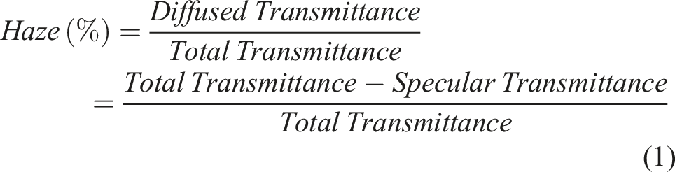
Figure 8 shows the total transmittance and haze of different nRRSs. The transmittance was measured based on a reference substrate (ITO-coated glass), and the haze was calculated based on the measured transmittance and derived. As shown in Figure 8(a), all the samples showed a very high transmittance of over 97% in the visible light wavelength range compared to the reference. As the nRRS sample has a multi-layered structure, the total transmittance exhibited oscillation owing to the interference effect at the layer interface. Therefore, to clearly examine the optical properties of the nRRS, characteristics of the samples were described with the average total transmittance and average haze, which were obtained by taking the average values measured at intervals of 1 nm in the specific wavelength range; visible light range (380–700 nm) and the green FWHM range (500–550 nm). The average total transmittance of each sample in the visible light wavelength range of 380–700 nm was as follows: planar (98.49%), R15 (98.37%), R20 (98.54%), R25 (98.72%), and R30 (98.00%). Since there was no difference except for the surface roughness between the sample, all samples showed similar average total transmittance values. However, the haze tended to increase as the number of rubbings increased, and the average haze in the 380–700 nm wavelength range was as follows: planar (−0.48%), R15 (3.00%), R20 (4.15%), R25 (9.27%), and R30 (18.09%). As the number of rubbings in a single direction is accumulated, the roughness and height of the nRRS increase, thereby making the contact surface with air wavy; thus, the probability of scattering the light path increases. Therefore, the light incident above the critical angle is not waveguided in the glass substrate but can be emitted in a random direction through the nanoscale jagged surface. R30, which had the largest maximum peak-to-valley height of 233 nm, exhibited the highest haze; thus, it was expected that the luminous efficiency improvement would be the best. The planar sample showed a lower haze than the reference ITO-coated glass substrate because of the rather thick SU-8 polymer. It is judged that the negative haze of the planar sample appeared by partially mitigating the random scattering resulting from the ITO grain boundaries, microscopic irregularities, or defects at the surface. Nevertheless, the scattering effect is almost negligible, as it shows a minuscule value of −0.48%. (a) Total transmittance (in solid lines) and haze (in dashed lines) of different nRRSs at 300–800 nm wavelength. (b) Average total transmittance and haze at 500–550 nm green FWHM wavelength.
Maximum peak-to-valley height (Rz), total transmittance and haze of different nRRSs.

aAverage total transmittance and haze at the green FWHM (500–550 nm).
EL characteristics
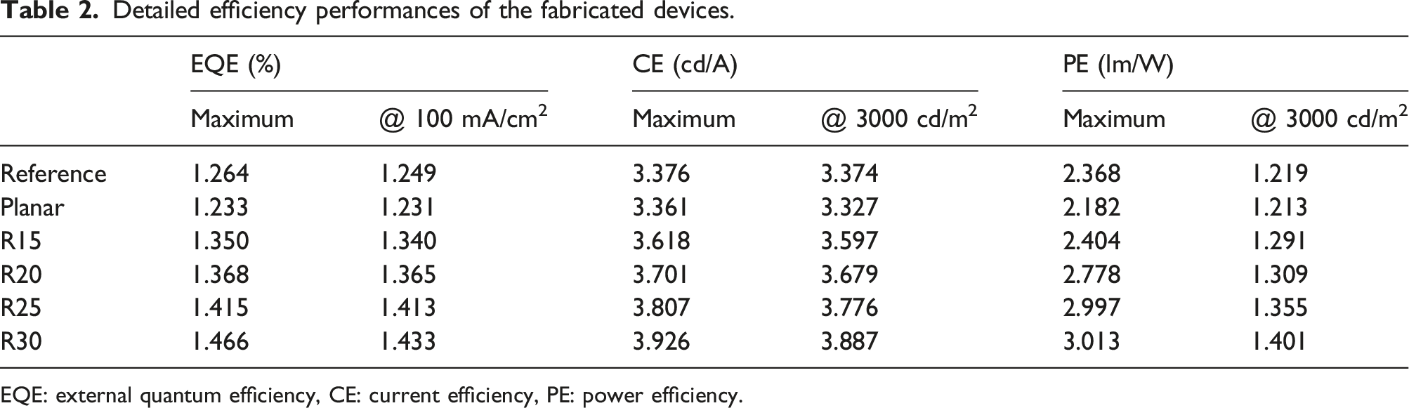
To compare the performance of the devices according to various nRRSs, the following OLEDs were fabricated: reference device (without SU-8 layer), planar device (with non-rubbed SU-8 layer), R15–OLED (15 times of rubbing), R20–OLED (20 times of rubbing), R25–OLED (25 times of rubbing), and R30–OLED (30 times of rubbing). The reference was a green fluorescent OLED device with no modification on the substrate surface, and the substrate was used as a 180 nm ITO-coated glass. Figure 9 shows the EL characteristics of the fabricated devices. As shown in Figure 9(a), there were no significant differences in the current density and luminance characteristics of the devices. Because the nRRS was applied outside the glass, the electrical operating properties were similar within the normal device range, and all the devices showed a brightness of 1000 cd/m2 at approximately 7.5 V. The efficiency factors of each device are shown in Figures 9(b) and (c). Because the planar device has a structure with a non-rubbed SU-8 polymer layer, the overall efficiency slightly decreased compared to the reference, as expected in the FDTD simulation. However, the nRRS‒OLEDs showed improved external quantum efficiency, current efficiency, and power efficiency compared to the reference owing to the scattering effect occurred by the nanostructure, and the substrate mode was partially converted to the air mode. Furthermore, as the height of the nRRS increased owing to the higher number of rubbings, light scattering appeared more effectively, resulting in larger haze; thus, the light extraction efficiency also increased. Compared with the reference, the R15, R20, R25, and R30 devices showed enhanced external quantum efficiency at 100 mA/cm2 of 7.29%, 9.29%, 13.13%, and 14.73%, respectively, in the normal direction. The current efficiencies of the R15, R20, R25, and R30 devices at 3000 cd/m2 improved by 6.61%, 9.04%, 11.91%, and 15.20%, respectively. The power efficiency of each device at 3000 cd/m2 improved by 5.91%, 7.38%, 11.16%, and 14.93%, respectively. As expected, the OLED combined with R30 exhibited the best device performance based on its excellent scattering effect. No pixel blurring phenomenon was confirmed, as shown in the inset of Figure 9(b). The detailed efficiency performance of the devices is presented in Table 2. The efficiency enhancement tendency according to the height of the nRRS showed the same result as that confirmed through the FDTD simulation. EL characteristics of the fabricated OLEDs. (a) Current density and luminance according to the voltage, (b) external quantum efficiency according to the current density (inset: photograph of the operating devices at the current density of 25 mA/cm2), and (c) current efficiency and power efficiency according to the luminance. Detailed efficiency performances of the fabricated devices. EQE: external quantum efficiency, CE: current efficiency, PE: power efficiency.
Viewing angle characteristics
The viewing-angle characteristics of each device at a current density of 100 mA/cm2 are shown in Figure 10. The reference and planar devices showed almost no difference from the ideal Lambertian emission profile. However, the nRRS–OLEDs showed an increase in the emission intensity compared to the reference at angles above the normal direction owing to the presence of a scattering layer. The wider distribution suggests that the scattering of light is effectively accomplished by the nRRS, and it can be observed that the distribution of light is rearranged in a random direction. Therefore, the light, which was originally waveguided in the glass substrate and lost, was emitted into the air, contributing to the improvement in the device performance. At a viewing angle of 60°, the normalized intensities of the R15, R20, R25, and R30 devices increased by 12.51%, 18.26%, 28.81%, and 26.05%, respectively, compared with the reference. Considering the deviation from the Lambertian distribution from 0° to 70°, the external quantum efficiency of the R30–OLED was improved by 25.4%. R25–OLED, R20–OLED, and R15–OLED exhibited improvements of 23.7%, 16.8%, and 14.3%, respectively. Normalized EL intensity distribution of the fabricated devices. Angular distribution of each device was normalized at the maximum intensity.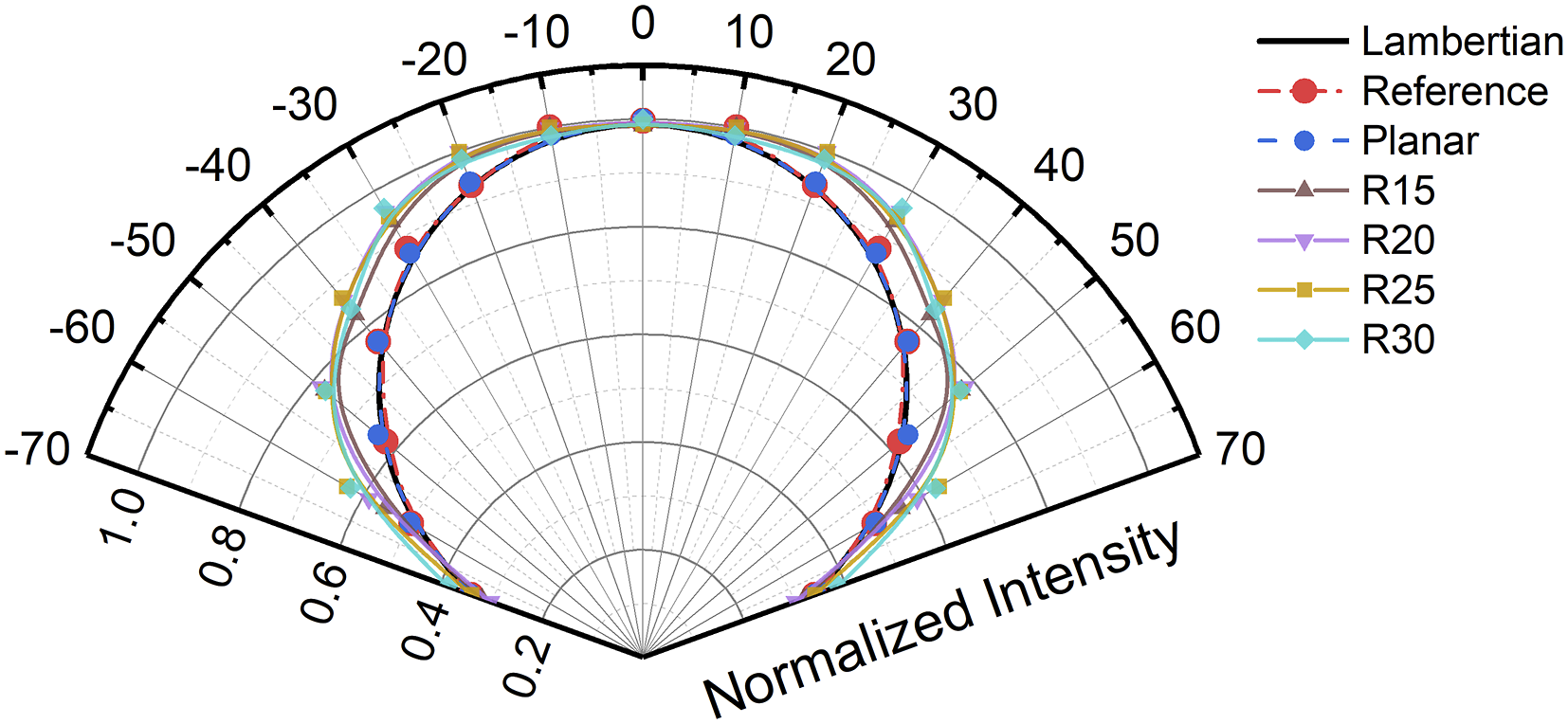
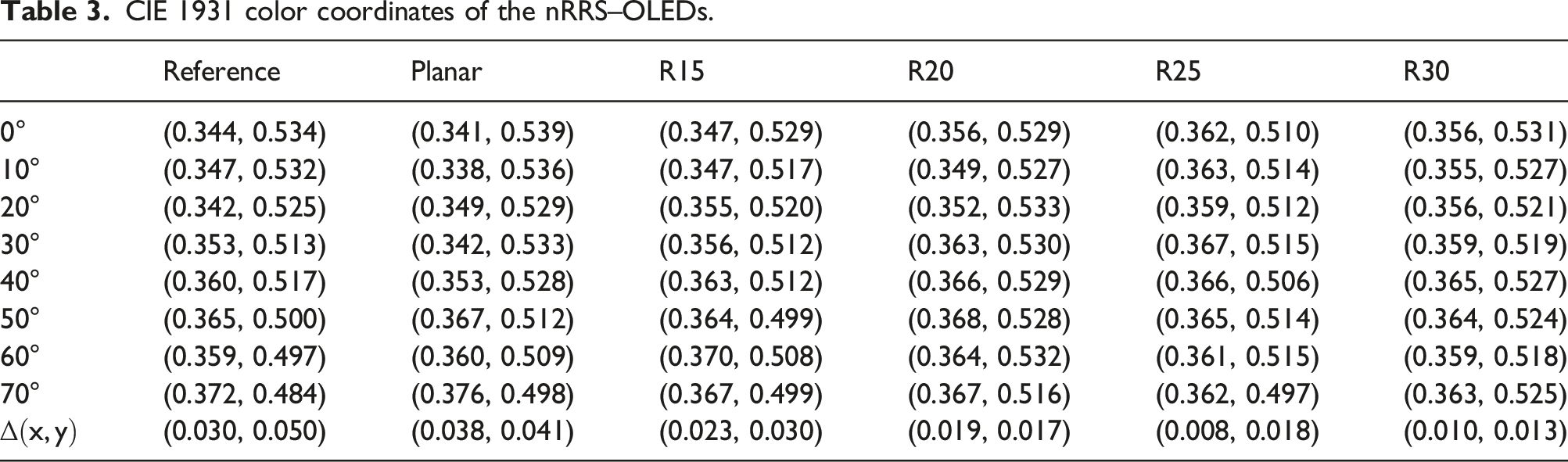
When a periodic nanostructure is used as the light-extraction structure, the spectrum distortion phenomenon, in which the color changes depending on the viewing angle, occurs as a critical disadvantage. However, because the nRRS has a nanosized structure, it extracts light in the visible region and simultaneously has a random distribution; thus, it has the advantage of suppressing the viewing angle characteristics. To confirm the alleviation of the angular color shift, the coordinate difference according to the viewing angle in the CIE 1931 color space was examined, as shown in Figure 11 and Table 3. We defined the CIE 1931 coordinate difference CIE 1931 color coordinate shifts according to the viewing angle. CIE 1931 color coordinates of the nRRS–OLEDs.
Conclusions
In this study, the performance enhancement was evaluated by fabricating a nanoscale random structure as a scattering layer that can improve the light extraction efficiency of OLEDs using the rubbing technique, which is mainly used only for liquid crystal alignment. The rubbing technique has an excellent process advantage in that it can form a large-area nanostructure under room temperature and normal pressure conditions, and the nRRS produced through rubbing has a random distribution over all areas. Additionally, the nRRS could be engineered by controlling the rubbing process, and the scattering effect according to the roughness and height of the nRRS was analyzed through FDTD simulation and confirmed through the fabricated device. The nRRS played a role in improving the optical efficiency by rearranging the path of the light waveguided by the total internal reflection at the substrate and air interface. The optimized nRRS showed a high transmittance of 97.8% and haze of 17.8%, which is suitable for use as a scattering layer for OLEDs. The device combined with the optimized nRRS showed an improvement in the external quantum efficiency of 25.4% compared to the reference. Owing to the scattering effect, the angular distribution of the nRRS OLEDs deviated slightly from the Lambertian profile, but the CIE 1931 coordinate difference according to the angle was diminished, thereby alleviating the spectrum distortion caused by the change in the viewing angle. The approach to fabricating random nanostructures through the simple and inexpensive process investigated in this study is expected to be utilized not only in OLEDs but also in various optical devices. Our previous study, in which a low-height nRRS was inserted inside the device, had limitations in engineering because many factors had to be considered for normal device operation. However, in this study, there are infinite possibilities in that beneficial optical effects can be derived more simply by combining the nRRS outside the device. Owing to its cost-effective, high productivity, and mask-free manufacturing characteristics, the nRRS is expected to be applicable to numerous fields requiring light path redistribution, and since it does not require high temperature, it will also be able to expand to deformable devices.
Supplemental Material
Supplemental Material - Enhancing the optical performance of organic light-emitting diodes using nanoscale random rubbed structure
Supplemental Material for Enhancing the optical performance of organic light-emitting diodes using nanoscale random rubbed structure by Cheol Shin, Seungwon Lee, Kwang Wook Choi, Young Hyun Hwang, Young Wook Park and Byeong-Kwon Ju in Nanomaterials and Nanotechnology
Footnotes
Declaration of conflicting interests
The author(s) declared no potential conflicts of interest with respect to the research, authorship, and/or publication of this article.
Funding
This work was supported by Samsung Display Co, Ltd, the National Research Foundation of Korea (NRF) grant funded by the Korean Government (MSIT) (No. NRF-2020R1C1C1013567), and the Brain Korea 21 Project in 2021.
Supplemental Material
Supplemental material for this article is available online.
References
Supplementary Material
Please find the following supplemental material available below.
For Open Access articles published under a Creative Commons License, all supplemental material carries the same license as the article it is associated with.
For non-Open Access articles published, all supplemental material carries a non-exclusive license, and permission requests for re-use of supplemental material or any part of supplemental material shall be sent directly to the copyright owner as specified in the copyright notice associated with the article.