
Abstract
We demonstrate how the formation of octahedral microcrystals of arsenic oxide As2O3 in the form of arsenolite with a size of 200 nm to 10 μm can be initiated by the electrochemical etching method with simultaneous deposition on the surface of substrates with n-GaAs (111). Crystallites were formed on a previously synthesized porous layer of GaAs. To explain the behavior of formation on the surface of the monocrystalline GaAs porous layer and As2O3 crystallites in the electrochemical reaction, we propose a qualitative model based on the decomposition of binary semiconductors in contact with electrolytes. Under this model, the crystallization of precipitated oxides occurs as a result of the transfer of ions to the crystal surface as a result of the electrolysis process. The formation of the composite structure takes place on the surface of the semiconductor and is characterized by the minimization of elastic energy. XRD analysis showed the formation of a complex compound of As2O3 and As0.172Sb0.570O1.113. The appearance of antimony is explained in terms of the formation of new centers when the As atom is replaced by an Sb doping atom in the crystal. Directed controlled oxidation technologies make it possible to synthesize a reliable passivating layer consisting of one type of oxide, namely As2O3 in the cubic phase of arsenolite. In addition, such structures can be used in photonics devices and as photocatalysts.
Keywords
Introduction
Recently, the efforts of researchers and engineers have aimed at optimizing and improving the methods of synthesis of new functional materials.1–3 Nano- and microstructured semiconductors are widely used in modern laser technologies, solar cells, as sensors and supercapacitor plates.4–9 An important technological task is to simplify and reduce the cost of synthesis technologies. In this regard, methods for electrochemical structuring of the surface are being actively developed.10,11 It is important to mention that the electrochemical etching method is intensively used for nanostructure synthesis in the so-called ion-track template, which made it possible to create different nanocrystalline surface structures based on ZnO, ZnSeO3, CdTe, CdO and so on.12–14 These methods have significant advantages over epitaxial and lithographic, in particular: no mechanical, thermal, and ionic effects on the sample surface, no tool wear, extremely wide control over the geometric shape (architecture) and size of micro- and nanostructures.15,16 The undeniable advantages of the methods are simplicity, a small number of parts of the technological process, no need for complex equipment and low cost of technological operations.
Conventionally, electrochemical treatment can be divided into subtractive (local removal of material from the sample volume) and additive (local deposition of material on the sample surface).17,18 Recently, combined methods have been actively developed that allow the simultaneous formation of nano-relief both in volume and on the surface of the sample.19,20
Electrochemical treatment methods are effective for the creation of porous substrates, nanoneedles, nanowires, crystallites and micro islands.21–23 The creation of whiskers, threads, spots, etc. has been reported many times.24–26 Thus, electrochemical treatment is an effective method for the synthesis of 1D, 2D and 3D structures. Recently, it has been customary to study such porous materials and free volumes using the positron annihilation method.27,28 However, there are a number of disadvantages of chemical and electrochemical treatment methods; the key disadvantage is poor reproducibility of results.
Electrochemical deposition of coatings is one for the effective methods of modifying the microstructure and properties of modern functional materials. 29 Composite coatings that contain oxide particles in the semiconductor matrix often have improved functional properties compared to monocrystalline analogues. 30 The influence of crystalline oxide inclusions on the electrical, magnetic, thermophysical properties of the material correlates with their composition, size, coating density, and morphological structure. 31 Today, the deposition of metal components from electrolytes containing nanoparticles resistant to aggregation or dissolution is promising. 32 The use of colloidal electrolytes has often been reported, from which nanoparticles are effectively incorporated into the matrix of the original sample, resulting in a change in structure and properties. 33 However, such colloidal electrolytes are often characterized by the instability of colloidal particles in the aggregation.
Electrochemical methods of electrodeposition are traditionally used to obtain thin films, nanoneedles and nanowires, in particular in the dimensional electrochemical deposition of metal perpendicular to the surface of the sample in the pores or microplate of the template.34,35 Glass, polycarbonate membranes, porous materials can be used as a template.36,37 For example, porous alumina is an ideal candidate for the synthesis of nanomaterials due to homogeneous porosity.38,39
The main tasks facing researchers face, are: - establish conditions of uniform electrodeposition both on thickness, and on a surface of a semiconductor plate; - forecast the growth rate of layers and structures; - determine the nature of the restricted growth rate and study the process kinetics.
It should also be noted that the micro and macro-morphology of the surface, the thickness of the films, and the component composition can vary greatly depending on the conditions and parameters of electrochemical treatment of semiconductor wafers.
However, the formation of ordered nanocrystallites on the surface of semiconductors may be of particular interest for the obtaining composite materials that have unique properties. The problem is the choice of template, which has a number of requirements and restrictions, in particular, the consistency of the crystal lattice.40,41
In this sense, in our opinion, the most promising substrates can be considered those that have a chemical affinity for synthesized nanocrystallites.42,43 This ensures the adsorption of crystallites on the surface of the semiconductor, which is essential for their effective incorporation into the substrate matrix. 44
The purpose of this study was to determine the mechanisms of synthesis and study the properties of oxide crystallites on the surface of gallium arsenide. We study the conditions of crystal formation on the surface of GaAs, analyze the main factors influencing this process, and investigate the composition and phase parameters of oxide components. These results make it possible to control the process of etching and electrochemical deposition to obtain porous nanostructured layers on the surface of gallium arsenide with or without these crystalline structures.
The main difference between our proposed method and the previous studies discussed above is the use of a combination of electrochemical deposition and etching. This allows the formation of an intermediate porous layer of GaAs, which is a buffer for the deposited layer of crystallites. In this way, we solve the problem of selecting a template for the formation of a crystalline sediment, which is represented by diamond-type microcrystallites.
Samples and experiment
Initial characteristics of the samples for the experiment.

The structures were formed by electrochemical etching technology with simultaneous electrochemical deposition. A standard two-electrode electrolytic cell was used for this purpose. Platinum with a diameter of 1 cm was used as the insoluble electrode (cathode). The experiment was carried out at room temperature in daylight.
The formation of crystallites was carried out in several steps: Step 1. Electrochemical etching in the H2O:H2SO4=10:1 (by volume) solution at constant voltage U1=6 V to form a porous layer on the surface of monocrystalline GaAs. Active separation of bubbles at the anode (sample GaAs) and the cathode (Pt) was observed. This stage was characterized by a sharp increase in current density to values of j1=170 mA/cm2. After 3 min, the current stopped rising, the electrolyte became light pink, and the surface of the sample became matte. A dark plaque appeared on the platinum. It is logical to assume that at this stage there was an active pore formation with the release of arsenic and gallium into the electrolyte solution. Step 2. Electrochemical deposition method was used to initiate cathodic deposition. In the same electrolyte solution was added 1 part ethanol (C2H5OH) and 1 part of nitric acid (HNO3). Thus, the electrolyte concentration by volume was: H2O:H2SO4:C2H5OH:HNO3=10:1:1:1. The potential of the working electrode was maintained at approximately U2 = 10 V to prevent both large-scale deposition of oxides and dissolution of the precipitate. During the experiment, active electrolysis of the solution with the release of oxygen bubbles was observed. On the one hand, the movement of bubbles creates convection of the electrolyte, and thus increases the allowable rate of electrodeposition of metal sludge. On the other hand, bubbles increase the resistance of the medium in the interelectrode space. Therefore, mixing the electrolyte with a Teflon stirrer was used to reduce the effect of bubbles on the electrochemical deposition process. The duration of the stage is 4 min. During this stage, the platinum was cleaned of plaque. Step 3. Exposure of the samples in the same electrolyte solution without applying the potential for 3 min to stabilize the formed structures. The samples had a uniform dark blue color and a matte surface.
After the experiment, the samples were washed in an alcoholic solution and kept in air for 1 month.
The surface morphology was examined on a SEO-SEM Inspect S50-B scanning electron microscope. Energy dispersion analysis was performed using an AZtecOne spectrometer with an X-MaxN20 detector (Oxford Instruments plc). Raman spectra were recorded using a RENISHAW inVia Reflex microscope when irradiated with a laser with a wavelength of 532 nm, and a lattice of 2400 nm, a range of 100–1000 cm-1. The measurement time was 10 s; 5 accumulations were performed. XRD analysis was performed on an XRD Drone-3M X-ray diffractometer Drone-3M in the range of angles 2
Experimental results and discussion
Morphology and mechanism of nanocrystallite formation
Figure 1 shows the morphology of the gallium arsenide after electrochemical treatment. You can see that a loose porous layer formed on the surface of n-GaAs. The formation of this layer is a consequence of the first stage, namely the electrochemical etching of the crystal. N-type gallium arsenide lends itself well to electrochemical dissolution in acidic electrolytes. At the same time, a porous layer is formed on the surface as a result of the extraction of arsenide and gallium atoms. It can be seen that in some areas (Figure 1(a)), there is a certain anisotropy of the crystal etching. There are mutually parallel etching bands due to the orientation of the surface (111). The porous layer is not homogeneous, it consists of islands with a diameter of 3–7 μm (Figure 1(b)). Each island consists of small pores with a diameter of 80–200 nm (Figure1(c)). The pores do not show order and, therefore, do not depend on the crystallographic orientation of the crystal matrix (Figure 1(d)). This type of pore formation is called seeding; pores are formed over the entire surface without reference to the location of defects. The islands are separated by grooves (Figure 1(a)–(c)). Massive etched areas are observed at the junction of the islands. This type of pore is characterized as “butt pores”. Their appearance may be due to crystal dislocations, which are sources of diffusion, dislocation, and disclination stress concentrators. Relaxation of the butt hub can be carried out due to local accommodation at the junction of the two islands, in particular due to the formation of pores. The triple junction of the boundaries of the islands is formed by the intersection of three planes along a specific linear defect of the triple junction channel. SEM image of the surface of gallium arsenide after electrochemical treatment.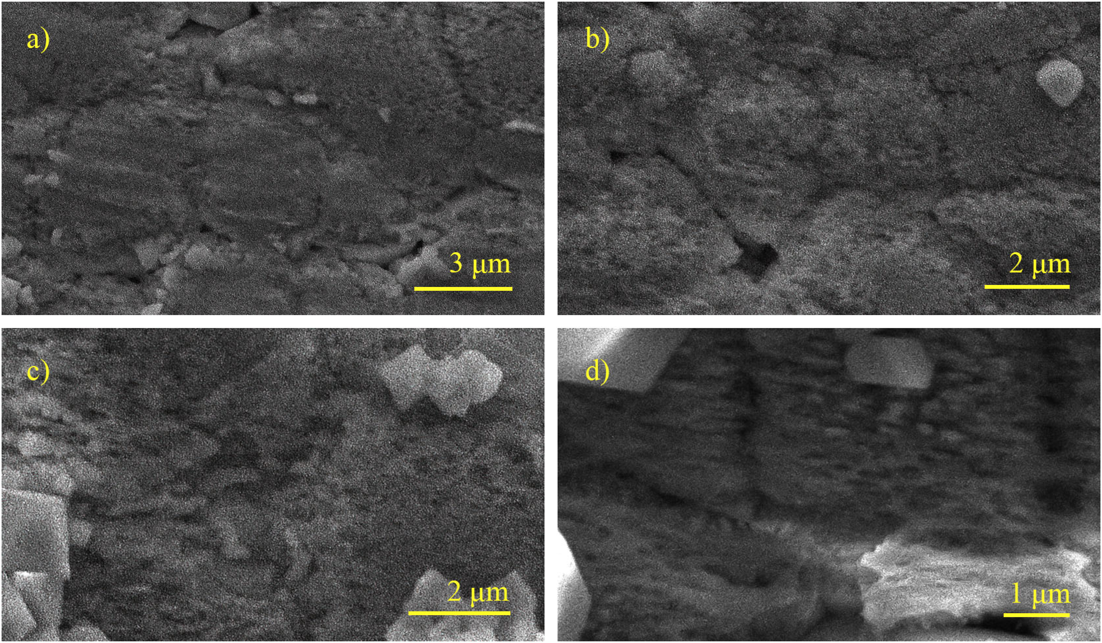
The described processes are characteristic of polycrystalline materials, while we used single-crystal GaAs in the experiment. Therefore, it can be assumed that the porous layer was formed not only by etching the material from a single crystal but is the result of a complex electrochemical process at the electrolyte/semiconductor interface. Such processes are usually accompanied by the formation of oxide compounds on the surface during electrochemical etching.45,46
After the complete process of electrochemical treatment of the crystal by scanning electron microscopy, it was found that octahedral crystallites with sharp edges dispersed on the surface of the porous layer (Figure 2). The size of the crystallites varies within (5 – 8) μm. SEM images of crystallites formed on the surface of gallium arsenide.
Nanocrystallites have a pyramidal morphology (tetragonal dipyramid) with a predominant orientation along the plane (111). This octahedral structure of crystals is characteristic of arsenic oxides, in particular As2O3. 47 Octahedral crystals indicate that arsenic oxide is in the bulk crystalline phase of arsenolite.
Microcrystals are formed because of the migration of arsenic ions and electrolyte components to the surface of the semiconductor wafer and deposition on the formed porous islands. It can also be stated that the crystals are formed and increase in size during electrochemical treatment of the crystal, even without removing the sample from the solution and exposure to air.
The scatter of crystallites in size indicates that their growth is due to the content of arsenic in the electrolyte solution and the migration of ions or arsenic oxide to the semiconductor plate as a result of an electric current and that this process is dynamic. The growth process of microcrystalline rocks is influenced by surface conditions and defects of the etched substrate.
Investigation of the chemical composition of surface layers and micro crystallites
According to the results of EDX spectroscopy (Figure 3), it was found that Ga, As, O, C atoms are present on the surface of the material. The spectra were taken at three points on the surface: (1) in a porous region free of crystallites; (2) an area with clearly formed octahedral crystallite; (3) an area with indistinctly formed massive crystallite. Table Figure 2 shows the relationship of the elements at three points on the surface of the structure. EDX spectra of the GaAs surface after electrochemical treatment.
The ratio of chemical elements on the surface of GaAs after electrochemical treatment, obtained by the EDX method.

The concentration of Ga at point (1) is also quite low (10.2%). Although preliminary data obtained by us and other researchers suggest that As sublattice is eroded from the surface of GaAs faster than Ga.48,49 From this we can draw a preliminary conclusion that during the electrochemical reaction, there was electrodeposition of arsenic oxide, the concentration of which in the electrolyte was much higher than that of gallium, in particular, due to the higher etching rate of As atoms. The porous surface, which is free of crystallites (point (1)), is most likely a complex compound GaxAsyOz, or consists of a set of compounds GaAs, Ga2O3, As2O3, As4О6 and the like.
The results shown in Figure 3, confirm that microcrystals have clear peaks for As and O, while nonmicrocrystalline porous regions show peaks for O, Ga and As. This also indicates that the crystallites are arsenic oxide. As2O3 may have a lower solubility than Ga2O3, leading to the formation of localized regions with arsenic oxide in the form of octahedral microcrystallites.50,51 In particular, the properties of gallium oxide and surface oxidation of gallium arsenide have been repeatedly reported.52–54
The ratio of components As and O at point (2) and (3) by weight is almost 3:1, respectively, by weight - 3:5. This ratio is characteristic of As2O3 oxide, which agrees well with the earlier assumption that crystallites are As2O3 in the crystalline form of arsenolite. At point (3) there is more arsenic, which indicates the dynamic process at the semiconductor/electrolyte interface during the electrochemical reaction.
Electrochemical mechanisms
To explain the behavior of the formation on the surface of the monocrystalline GaAs porous layer and arsenic oxide crystallites during the electrochemical reaction in the electrolyte-semiconductor system, we propose a qualitative model based on the decomposition of binary semiconductors in contact with electrolytes. The surface of compounds А3В
5
consists of layers with atoms of the third and fifth groups (in our case Ga and As, respectively). The layers alternate with each other. The GaAs {111} surface is characterized by the fact that all electrons in Ga atoms are paired, while As atoms have one or two pairs of electrons that do not participate in the formation of bonds (Figure 4). Model of electronic configuration of Ga (a) and As (b) atoms on the surface of GaAs {111} of sphalerite structure; (c) is a crystalline GaAs lattice of the sphalerite type.
Electrochemical dissolution of semiconductors depends significantly on the etching agents and the applied potential. 55 Dissolution of n-GaAs (111) in an electrolyte containing HNO3 occurs by mechanisms similar to dissolution of n-InP (111) in HF. 56 Earlier we reported the formation of crystallites on the surface of indium phosphide. Crystallites grew mainly in the places of concentration of defects. 57 Therefore, the first stage of crystal dissolution is characterized by the formation of adatoms: Ga+–NO3- and As-–H+ bonds replace GaAs surface bonds. 58 Thus, we have the formation of Gui-Helmholtz transition layers. 59 As a result of the applied potential, the adatoms break out of the crystal surface and pass into the electrolyte solution. It is probable that Ga+–NO3- adatoms are stable salts that settle at the anode or precipitate, while As-–H+ decompose to form elemental arsenic. The presence in free electrons of As atoms causes a reactivity higher than that of Ga, which causes faster etching of the arsenic sublattice. Then the electrolyte solution is saturated with arsenic atoms. The partially etched arsenic from the template is replaced by oxygen; a loose porous film of GaxAsyOz oxide is formed on the surface.
The electrolyte consists of acid solution ions and arsenic atoms, but such an electrolyte is already characterized by ion depletion. In addition, the surface of the semiconductor, as already mentioned, contains a Helmholtz-Guy transition layer, which can cause a passivating oxide film on the surface, which will characterize the completion of the electrochemical dissolution of the crystal. To increase the concentration of ions in the electrolyte in the second stage of electrochemical treatment, we additionally introduced ethanol and nitric acid into the electrolyte (as described in the “Experiment” section of this article). As a result of this process, the electrochemical dissolution of the crystal continued; at the same time, crystallites of arsenic oxide began to form on the surface. Arsenic oxide formation can occur by the following chemical reaction:
60

The disordered por-GaAs surface contains many surface states, which have become the nuclei of arsenic oxide crystals. This can also be seen in Figure 5, which shows that the crystallites are formed in the center of the oxide island. The explanation for this is the fact that in the center of the islands there is the greatest intensity of the crystal, while at the edges it is the lowest. SEM image of the porous GaAs surface with oxide crystallites.
Figure 6 shows a formation diagram of As2O3 octahedral crystals formed on the surface of gallium arsenide due to the conversion of As into As2O3 by convective diffusion. Furthermore, the electrochemical synthesis of As2O3 and the pore formation cannot occur simultaneously, leading to the formation of a complex multilayer compound mono-GaAs/por-GaxAsyOz/As2O3. Schematic representation of mono-GaAs/por-GaxAsyOz/As2O3.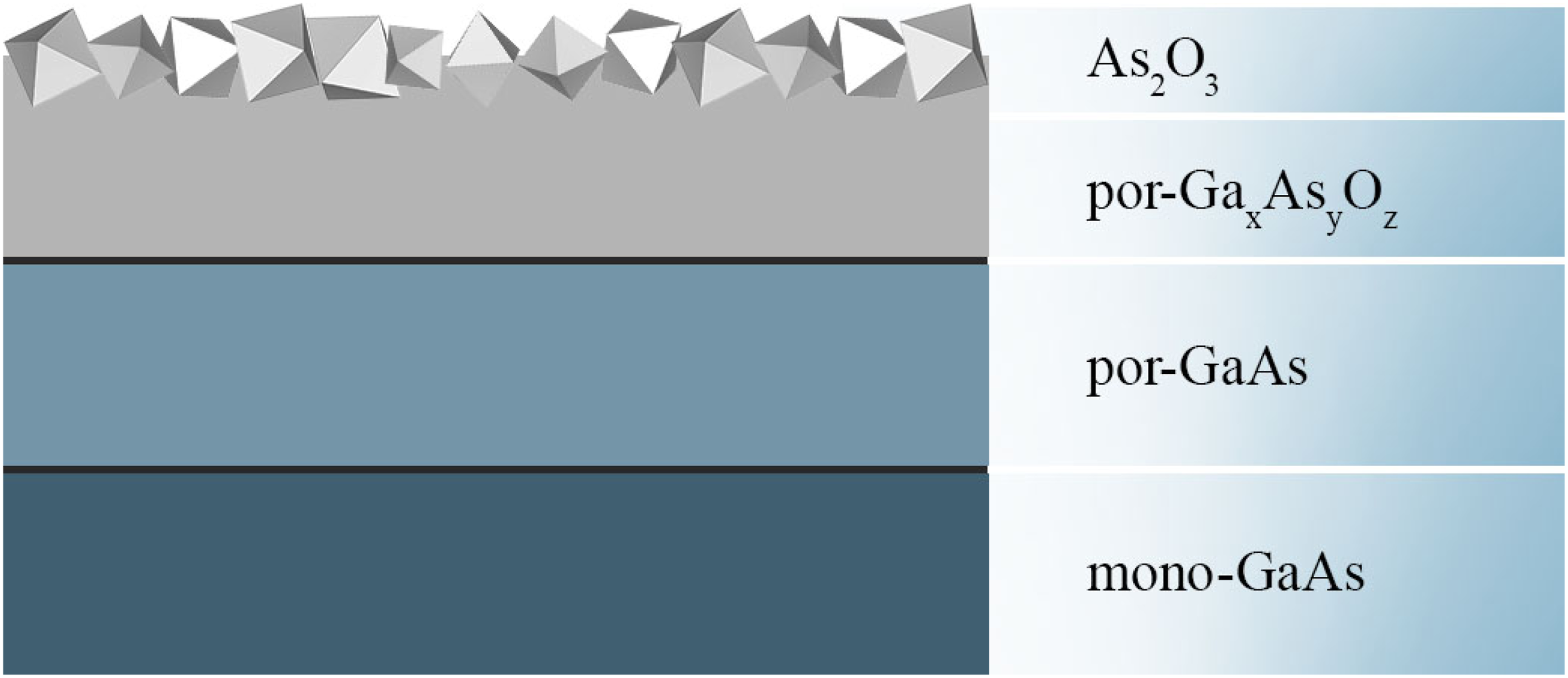
Thus, the formation of ordered crystallites refers to the phenomenon of self-assembly. Crystallization of precipitation oxides occurs as a result of the transfer of ions to the crystal surface as a result of the electrolysis process. The formation of the composite structure occurs on the semiconductor surface and is characterized by the minimized elastic energy. This is facilitated by the chemical affinity of nanocrystallites and the substrate material.
RAMAN-analysis
Figure 7 shows the Raman spectra of the formed material. Raman spectra show quite a few peaks, which may be due to the optical oscillations of arsenic and gallium oxides. The Raman spectrum can be divided into three groups: low-frequency mode (less than 200 cm-1), medium-frequency mode (200 - 300 cm-1), and high-frequency mode (more than 300 cm-1). Raman spectra of nanostructures synthesized on the mono-GaAs surface.
The peak 267 cm-1 corresponds to the frequencies of the transverse (ωTO) optical phonon of crystalline gallium arsenide, and the peak, located at 286 cm-1, is due to scattering from the phonon LO. In general, the peak at 268 cm-1 is a typical GaAs peak, in our case, it is slightly shifted to the low-frequency region of the spectrum due to the formation of a porous layer on the surface. This is also evidenced by the low-intensity broad peak in the area of 200 cm-1. The expansion of the peak occurs because of the heterogeneity of the porous structure and a significant variation in the size of the interporous walls. Instead, the peak is 287 cm-1. quite narrow and sharp, indicating a crystalline nature. The peak at 113 cm-1 may also indicate a porous structure, but its nature is not fully understood. Perhaps its appearance is due to the formed porous layer and oxide on the GaAs surface, as well as fluctuations in As-As.
The peaks at 368 cm-1 and 558 cm-1 indicate that the oxide crystallites synthesized on the GaAs surface consist of crystalline As2O3. It is proved by the fact that the peak has a rather narrow width. No trace of amorphous arsenic and elemental As was found. There is a shift of the oscillating bands of arsenic oxide to lower values relative to the volume values. This may indicate the presence of tensile stresses. This may also be due to the difference in the thermal expansion of GaAs and As2O3.
Thus, the results of the studied combination spectra are in good agreement with the results of scanning electron microscopy and energy analysis and confirm the previously made assumption that the octahedral crystals are arsenic oxide As2O3.
XRD-analysis
To determine the quantitative composition and the degree of crystallinity of the formed structures on the GaAs surface, we performed XRD measurements after anodizing. High-resolution spectra are shown in Figure 8. XRD analysis of the material clearly shows that it consists only of arsenic oxide and antimony elements. The Ga signal was completely gone. This is due to the predominant dissolution of Ga during electrochemical treatment, which leads to a much higher As/Ga ratio in the formed layers. Raman spectra of nanostructures synthesized on the mono-GaAs surface.
The peaks can be identified as a standard cubic structure of arsenolite (As2O3) with a lattice constant of 11.13 А° (a=11.13 А°, b=11.13 А°, c=11.13 А°; α=90o, β=90o, γ=90o). Within the detection limit of our method, no peaks are observed from other expected phases, such as GaAs (zincblende) or As4O6 (cubic oxide).
The appearance of antimony and the formation of the complex compound As2O3 and As0.172Sb0.570O1.113 can be explained as follows. As mentioned above, we used n-GaAs doped with Sb to a concentration of non-basic charge carriers 3 × 1019 cm-3. When the As atom is replaced by an Sb atom in the crystal, there occurs elastic deformation, which is due to the larger size of the antimony atom. The ratio of tetrahedral radii of atoms is the following:
This can change the lattice settings. That is, when a monocrystalline gallium arsenide is doped with an impurity Sb, a new center is introduced. The concentration of the new center depends on the concentration of Sb atoms. The concentration of non-basic charge carriers Sb is much lower than the concentration of As atoms, however, in all probability, the elastic field Sb leads to a more intense formation of centers around them. Thus, Sb initiates the appearance of a larger number of crystallites on the surface of the sample and, in a certain way, contributes to good crystallization of the obtained structure.
Virtually all peaks correspond to reflections from planes (222), (400) and (331) of the cubic phase As2O3 and As0.172Sb0.570O1.113.61,62 The intensity of the peak at 2ϑ=27.728о (222) is very strong, and its width at half the maximum is relatively narrow. On the basis of these arguments, it can be concluded that the sample shows a good state of crystallization as a result of the large size of crystals with a homogeneous content of O and As, which was previously confirmed by the results of SEM, XRD, and RAMAN.
At the end of this study, it is worth noting that intrinsic oxides of semiconductors are today considered reliable passivating layers that reduce the number of active centers on the surface, thereby preventing device degradation of devices.63,64 The main problem here is the amorphization of the surface.65,66 The combined method of electrochemical deposition of oxides on the surface of GaAs demonstrated by us makes it possible to obtain the crystalline form of its own oxide, namely As2O3. That is, directional oxidation makes it possible to create a passivating oxide layer that is uniform in volume and area of the sample and demonstrates a good degree of crystallinity. The optical properties of the formed structure require further research, which will open the prospects for the use of such materials in photonics devices. The developed morphology and unique microrelief may also contribute to the enhancement of photocatalytic performance, so this issue also needs further study.
Conclusions
The structural and chemical nature of the layers obtained by electrochemical etching with simultaneous electrodeposition of n-type GaAs has been studied. During the three-stage etching of the samples in a solution of nitric acid on the surface, a porous layer with tetrahedral crystallites of the correct shape was formed. The results of scanning electron microscopy, energy dispersion analysis and Raman scattering showed that the crystallites are arsenic oxide As2O3 in the crystalline form of arsenolite. The porous layer consists mainly of gallium arsenide and its complex oxides.
To explain the behavior of a porous layer on the surface of n-GaAs (111) and octahedral As2O3 crystallites during electrochemical treatment, a qualitative model based on the decomposition of binary semiconductors in contact with electrolytes has been proposed. It is shown that the formation of ordered crystallites belongs to the phenomenon of self-assembly. Crystallization of precipitation oxides occurs as a result of the transfer of ions to the crystal surface as a result of the electrolysis process. The formation of the composite structure occurs on the semiconductor surface and is characterized by a minimized elastic energy. This is facilitated by the chemical affinity of nanocrystallites and the substrate material.
X-Ray diffraction analysis of the crystallites clearly shows that they contain only elements of arsenic oxide and antimony. The Ga signal was completely gone. This is due to the predominant dissolution of Ga during electrochemical treatment, which leads to a much higher As/Ga ratio in the formed layers. The presence of antimony is due to the formation of new centers around the atoms of the alloying impurity.
Thus, we demonstrate that the method of electrochemical deposition in combination with the method of electrochemical etching allows the formation of high-crystallinity diamond-like oxide crystallites.
Footnotes
Acknowledgements
Ya. Suchikova thanks Goethe-Institut for supporting the House of Europe graduate emergency scholarship program. We also thank the Armed Forces of Ukraine for the safety in carrying out this work. This work was only possible due to the resilience and courage of the Ukrainian army.
Declaration of conflicting interests
The author(s) declared no potential conflicts of interest with respect to the research, authorship, and/or publication of this article.
Funding
The study was supported by the Ministry of Education and Science of Ukraine, that is: Project No. 0122U000129 The search for optimal conditions for nanostructure synthesis on the surface of A3B5, A2B6 semiconductors and silicon for photonics and solar energy and Project No. 0121U10942 Theoretical and methodological bases of system fundamentalization of the future nanomaterials experts training for productive professional activity.