
Abstract
The photogalvanic effect of monolayer SnS was investigated at a small bias voltage under perpendicular irradiation using density functional theory combined with the non-equilibrium Green’s function method. The photocurrent was generated over the entire visible light range, and it was saturated at a small bias voltage for photon energies of 2.4, 2.6, 3.2 and 3.4 eV. The photocurrent shows cosine dependence of the polarization angle, which is attributed to the second-order response to the photoelectric field. These results provide a deeper understanding of the photogalvanic properties of the 2D SnS nanosheet based devices.
Introduction
Two-dimensional (2D) materials, including graphene, transition metal dichalcogenides (TMDCs) and black phosphorus (BP), exhibit strikingly thermal, electronic and optical properties because their carrier migration and heat diffusion are confined to the two-dimensional plane.1-4 The unique properties of these materials have shown great potential for applications in energy storage, adsorption, catalysis and photoelectricity.5-7 2D materials have been widely applied for photodetection in the field of optoelectronics.8-13 For example, ultra-broadband graphene photodetectors have shown high responsivity at room temperature. 14 TMDCs such as MoS2, MoSe2, WS2, WSe2, etc., have been of the utmost interest due to their properties of finite bandgap, flexible, ultrathin and a wide variety of electronic properties ranging from metallic to semi-metallic to semiconducting. These superior properties make TMDCs a promising new materials for innovative sensors, optoelectronic devices, highly sensitive photodetection, quantum communication devices, and so on.15-19 Recently, black phosphorus photodetector has been demonstrated that it can operate under bias with a very low dark current and attain an intrinsic responsivity up to 135 mA W−1 and 657 mA W−1 in 11.5 nm and 100 nm thick devices at room temperature. 20 With the advent of the post molar era, there is a growing demand for nanodevices with high response and sensitivity.21-23 Therefore, the search for new semiconductor-based alternative materials has become a hot research topic.
Two-dimensional SnS belongs to a family of layered orthorhombic group IV-Ⅵ compounds including SnSe, SnS, GeSe, and GeS, all of which have similar puckered lattice structure similar to black phosphorus. Recently, 2D SnS has attracted widespread interest because of its unique properties such as adjustable direct band gap, high carrier mobility and in-plane anisotropy.24-26 Because these monochalcogenides are composed of two elements with different electronegativities, instead of one element in phosphorene, the inversion symmetry of the odd-numbered layers is broken. These characteristics result in richer physical properties than phosphorene. In recent time, many experimental studies of 2D SnS have been conducted. High quality SnS crystals synthesized by physical and chemical methods exhibit intrinsic polarization and an odd-and-even effect in terms of their layer dependence. 27 Zhang et al. reported that they synthesized single crystalline rectangle 2D SnS nanosheets using a conventional physical vapor deposition (PVD) method and fabricated near infrared photodetectors. 28 On the other hand, because the structures of 2D monochalcogenides are similar to phosphorenes, their properties have aroused great theoretical research interest. Many peculiar phenomena have been predicted, including valley-related transmission excited by linearly polarized light, 29 reversible in-plane anisotropic switching through strain or electric field, 30 etc. Through the first-principles calculations, it was found that the indirect band gap of some 2D monochalcogenides can be converted into a direct band gap by applying a small strain.31,32 However, to the best of our knowledge, there have been no reports on the photocurrent transport behavior of 2D monochalcogenides.
In this work, we studied the photocurrent of the SnS photodetector under linearly polarized light over the entire visible light range to explore the potential of SnS in optoelectronics. This reveals the dependence of the photocurrent on the light polarization under a small bias voltage. The results show that the photocurrent has a strong correlation with light polarization as well as broadband and anisotropic light responses. These results indicate that SnS is a promising candidate for photodetection in the visible light range.
Model system and theoretical methods
The optimized cell parameters for SnS are a = 4.083 Å and b = 4.294 Å, which are in full agreement with previous reports.33-35 A two-probe device model was built for the zigzag and armchair directions of SnS to study its photocurrent properties. Figure 1 shows the top and side views of the SnS photodetector in the zigzag and armchair directions. The device consisted of a scattering region, left and right leads. As shown in Figure 1, the x and y axis are set along the zigzag and armchair directions respectively, and the scattering regions are inside the red box. The photocurrent flows from the left lead to the right lead through the scattering region. The top and side views of Two-probe devices for calculating the photocurrent of monolayer SnS along the (a, b) zigzag and (c, d) armchair directions. The incident light is irradiated perpendicularly to the device along the z direction and polarized in the x-y plane. The angle θ represents the polarization angle relative to the zigzag (x) direction.
Twenty atoms of the whole scattering region were irradiated with linearly polarized light which propagates along the z direction perpendicular to the 2D monolayer SnS to obtain the photocurrent. A small bias voltage is applied between the two leads in order to give rise to a persistent photocurrent. The light is polarized in the x-y plane with the polarization vector forming an angle θ with respect to the x direction. The light polarization vectors
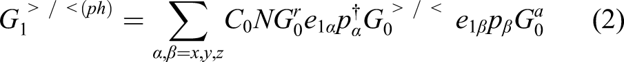
The density of states (DOS) and the band structure were calculated using the nanodcal36,37 package with GGA_PBE96 for the exchange correlation functional, and atomic cores are defined by the standard norm conserving nonlocal pseudopotentials. The photocurrent was calculated using the nanodcal package which applied density functional theory with Keldysh nonequilibrium Green’s Function theory (NEGF-DFT). The photocurrent of the left electrode for linearly polarized light


The normalized photocurrent (photoresponse function) can be written as

The photogalvanic effect along the armchair and zigzag directions were calculated at different θ and voltages for visible light, with photon energies ranging from 1.4 to 3.4 eV with an interval of 0.1 eV.
Results and discussion
The photocurrent was calculated at small biases from 0 V to 0.1 V with an interval of 0.01 V, and 0.1 V to 1 V with an interval of 0.1 V. The entire scattering region of the device was irradiated with linearly polarized light, which spread along the z direction. The photoresponses along the armchair and zigzag directions were generated at different θ for the photon energies which covers the entire visible light ranging from 1.4 to 3.4 eV with an interval of 0.1 eV. The electronic band structure of SnS is shown in Figure 2. In this work, the monolayer 2D SnS is an indirect band gap material of 1.46 eV, which agrees well with previous works,33,40,41 and is close to the experimental results.42-44 Electronic band structure of monolayer SnS.
Figure 3 shows the photocurrent in the armchair and zigzag directions at the voltage of 0.1 V for photo energies of 2.2 eV, 2.5 eV, 3.0 eV and 3.2 eV as examples. This shows that the photocurrent in the armchair and zigzag directions varies depending on cos (2θ). This response of the photocurrent can be deduced from equation (1), where the photocurrent includes three components, that are proportional to The calculated photocurrent at a bias voltage of 0.1 V for different photo energy in the (a) armchair and (b) zigzag directions.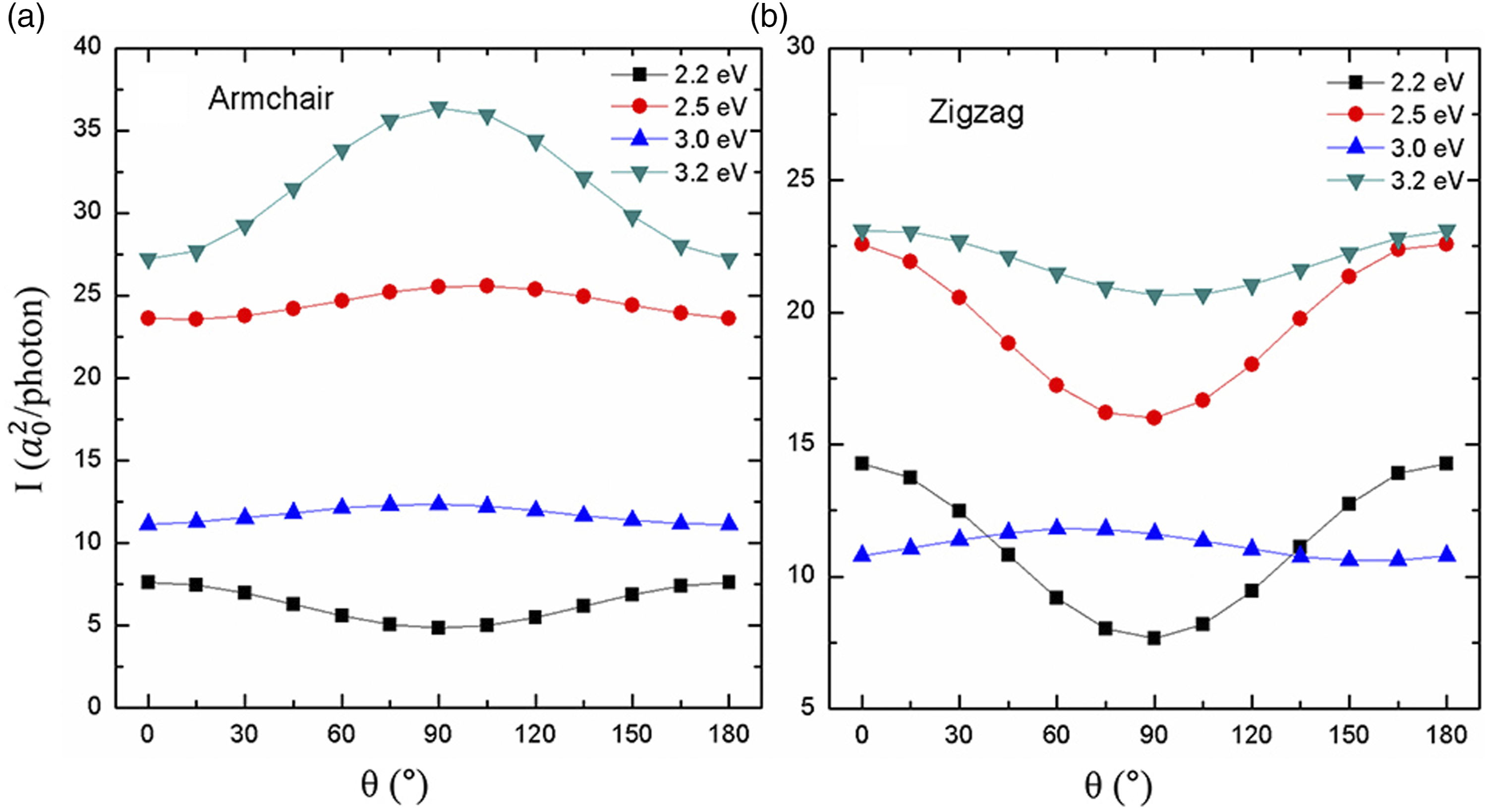
Figure 4 shows the maximum photocurrent Im as a function of photon energy in the armchair and zigzag directions under a small bias of 0 V − 0.09 V. The results showed that the photocurrent value under a voltage of 0 V was very small in both the armchair and zigzag directions, and the maximum value was 0.1 order of magnitude. As shown in Figure 4, the photocurrent generated by the photon energy approximating the band gap (1.4 – 1.5 eV) is very small. There are multiple peaks of Im in the range of 1.6–3.4 eV, the maximum peaks are at 2.4 eV, 3.2 eV in the armchair direction and at 2.4 eV, 3.3 eV in the zigzag direction, respectively. For the same photon energy, Im increases with an increase in the bias voltage. The maximum photocurrent (Im) varies with the photon energy in different bias voltages in the (a) armchair and (b) zigzag directions, respectively.
Figure 5 shows that the maximum photocurrent Im varies with different bias voltages in the armchair and zigzag directions. As shown in Figure 5(a), in the armchair direction, Im are small and saturate at very small bias voltages for the low photon energy of 1.4, 1.6, 1.8 and 2.0 eV. For photon energies of 2.4 and 3.2 eV, Im increase sharply with increasing bias voltage and reach a maximum value at 0.1 and 0.2 V, respectively. This is in full agreement with our results in Figure 4 for the variation of photocurrent at different photon energies. To have a deeper understanding, we calculated the density of states (DOS) and dielectric function of SnS, as shown in Figure 6. The energy gap between DOS peaks are around 2.4 and 3.2 eV as shown in Figure 6(a), and there are two peaks around 2.4 and 3.2 eV in the real part and imaginary part as shown in Figure 6(b). Therefore, 2D SnS devices generate large photocurrents by absorbing photons with energies of 2.4 and 3.2 eV. For photon energies of 2.8 and 3.0 eV, Im increase monotonically with increasing bias voltage and do not reach saturation value at 1V bias voltage. Since electrons excited by photons of different energies are transported in different channels, the saturation voltage varies with photon energy. Based on the imaginary part of the dielectric function, as shown in Figure 6(b), the resonant absorption of photons in the energy range of 2.6 eV to 3.1 eV is relatively small, resulting in reduced generation of excited carriers. However, applying an external bias voltage can induce more free carriers. Therefore, the photon current increases with the applied bias voltage at photon energies of 2.8 eV and 3.0 eV. The variation of Im in the zigzag direction with the bias voltage is the same as that in the armchair direction, as shown in Figure 5(b). The maximum photocurrent (Im) varies with the bias voltage in different photon energy in the (a) armchair and (b) zigzag directions, respectively. (a) Density of states (DOS) and (b) dielectric function of SnS.

To explain the above results, we calculated the density of states (DOS) and dielectric function of SnS, as shown in Figure 6. Figure 6(a) shows that there are three peaks in the conduction bands around 1.3, 1.7 and 2.15 eV above the Fermi energy (0 eV), and two DOS peaks in the valance bands around −1.15 and −1.45 eV below the Fermi energy. According to the Fermi golden rule, the transition rate is directly proportional to the DOS; therefore, a high electronic transition rate is achieved between one DOS peak in the conduction bands and another peak in the valence bands. The energy gap between these peaks are around 2.4 and 3.2 eV. Therefore, 2D SnS devices generate large photocurrents by absorbing photons with energies of approximately 2.4 and 3.2 eV. This is completely consistent with our results of the photocurrent change with different photon energies in Figure 4 and Figure 5, which produces a large photocurrent at energies around 2.4 eV and 3.2 eV. To gain a deeper understanding of the mechanism of the photocurrent change with incident photon energy, we calculated the dielectric function of SnS, as shown in Figure 6(b). There are peaks around 2.4 and 3.2 eV in the real part and imaginary part. This is in good agreement with our photocurrent results. Electrons and carriers are generated in the conduction band and valence band when 2D materials absorb photons, and they move in opposite directions under the action of a bias voltage to form a photocurrent.
Conclusion
In summary, we studied the photocurrent of a monolayer 2D SnS device using the atomic first principles method. The photocurrent was generated by linearly polarized light under a small bias voltage in the armchair and zigzag directions over the entire visible light range. The photocurrent changes observed in the shape of cos (2θ) with the polarization angle, agree well with the phenomenological formula often used in literature. The photocurrent had a larger value in the range of 2.2–3.4 eV photon energy, and there were two peaks near 2.4 and 3.2 eV. Under the same photon energy, the photocurrent increased with the bias voltage. Under certain photon energy, such as 3.2 eV, the photocurrent increased with the bias voltage and then reached saturation. We provide a satisfactory explanation for the behavior of the photocurrent, which is achieved using a combination of analysis of the density of states and dielectric. In short, we can effectively control the photocurrent in two-dimensional photovoltaic devices by changing the photon energy, bias voltage and polarization angle. This theoretical work may open up a new avenue for photovoltaic and photovoltaic applications involving monolayer SnS.
Footnotes
Declaration of conflicting interests
The author(s) declared no potential conflicts of interest with respect to the research, authorship, and/or publication of this article.
Funding
The author(s) disclosed receipt of the following financial support for the research, authorship, and/or publication of this article: This work is financially supported by the National Natural Science Foundation of China (Grant No. 51973046), the National Natural Science Foundation of China (Grant No. 11974091), and the National Natural Science Foundation of China (Grant No. 22108051).