
Abstract
Manganese-doped nickel oxide nanosheet array films are successfully prepared on a nickel oxide seed-coated glass substrate by an immersion method. Various annealing temperatures between 300°C and 500°C are applied to the manganese-doped nickel oxide nanosheet array films to study their effect on the properties of nickel oxide, including humidity sensing performance. Field emission scanning electron microscopy (FESEM), energy dispersive X-ray spectroscopy (EDS), X-ray diffraction (XRD), ultraviolet–visible (UV–vis) spectrophotometry, a two-probe current–voltage (I-V) measurement system and a humidity measurement system are used to characterise the heat-treated manganese-doped nickel oxide samples. The effect of annealing temperature can be clearly observed for the different surface morphologies and diffraction patterns. The samples exhibit average crystallite size increases of 0.63–10.13 nm with increasing annealing temperature. The dislocation density, interplanar spacing, lattice parameter, unit cell volume and stress/strain are also determined from the XRD data. The average transmittances in the visible region for all samples show low percentages with the highest transparency of 50.7% recorded for manganese-doped nickel oxide annealed at 500°C. The optical band gap shows a decreasing trend with increasing annealing temperature. The I-V measurement results reveal that manganese-doped nickel oxide displays improved conductivity values with increasing annealing temperature. The sensitivity of the humidity sensors shows an ascending curve with increasing temperature. The optimal device performance is obtained with annealing at 500°C, with the highest sensitivity of 270 and the fastest response and recovery times. In contrast, the sample for annealing at 300°C shows poor sensing performance.
Keywords
Introduction
Humidity sensors are devices that are in high demand for environmental and medical applications, as well as sectors that include the electronics, food processing and automotive industries. It is imperative to accurately and efficiently detect the percentage of water molecules in the environment. High sensitivity and stability are essential for benchmarking in humidity sensor measurements. The major drawbacks in the repeatability and reliability of sensors can limit their large-scale commercial applications. 1 Nanostructures with large surface-to-volume ratios and high active sites lead to greater and faster reactions in sensing activity. 2,3 Such nanostructured materials contain many defects, including structural and composite defects. 4 Significant efforts have been focused on the development of semiconductors, particularly metal oxides, to enhance high-performance humidity sensors. Metal-oxide semiconductors have certain advantages in terms of fabrication, such as low cost, simple and non-time-consuming processes. 1
Nickel oxide (NiO)-based humidity sensors have demonstrated significant potential and several advantages, even though NiO is categorised as a p-type semiconductor. This behaviour is due to Ni vacancies or doping with other cations. 5 –7 Parimon et al. reported NiO-based humidity sensors designed on seedless and seed-coated glass substrates with high sensitivities of 138 and 257, respectively. 8,9 In addition, the authors also successfully fabricated hierarchical NiO nanosheet/nanoball-flower-like structure films for humidity sensors at low immersion temperatures with a highest sensitivity of 169. 10 However, these previous reports used single NiO compounds rather than heterostructures and composite techniques for the application of humidity sensors. With regard to doping, Farooq et al. reported 0–20% manganese-doped nickel oxide (Mn-doped NiO) synthesised using a solid-state reaction method for use in humidity sensors. 11 The sensitivity values obtained were 9, 55 and 34 for 0%, 10% and 20% Mn doping, respectively.
NiO has many attractive properties that can be explored with a modification in experimental parameters. The addition of dopants during the preparation of NiO is one of many approaches that can yield exciting and enhanced characteristics in this material. For instance, the magnetic structure of NiO can be improved by doping with transition metals. 5 In a previous report, the metal doping of NiO resulted in improved sensor performance and good energy storage capacity. 12 In addition, the performance of several other applications of NiO, such as electrochromic devices 13 and perovskite solar cells, 14 was also improved by doping. Various metals have been investigated as dopants, including Al, 4,15 Zn, 13 Li, 14 Sn 16 and Mn, 17,18 to improve the properties of NiO. In particular, the combination of Mn with NiO has attracted significant attention due to its distinctive magnetic properties. The observed magnetic behaviour results from the dopant cation (Mn2+) occupying the Ni2+ sites in the lattice. 5
Reports of the different annealing temperatures of Mn-doped NiO, particularly for humidity sensor applications, are scarce, and this is especially true for Mn-doped NiO nanosheet array films grown directly on glass substrates. Many previous reports only compare the characteristics of NiO films at different Mn concentrations. For example, Mallick et al. studied the antiferromagnetic to superparamagnetic transition in NiO as a function of Mn doping (0–5 at.%). 5 Antiferromagnetic properties were observed for undoped and 1 at.% Mn-doped NiO samples, while at higher concentrations of Mn, superparamagnetic behaviour was induced. Furthermore, Layek and Verma successfully synthesised Mn-doped (0–6 at%) NiO nanoparticles in powder structure using a low-temperature hydrothermal method. 6 The introduction of Mn in the NiO lattice greatly enhances its magnetic properties at room temperature. Patel et al. also conducted the same percentages of Mn (0–6 at%) to study their effect on the structural, vibrational and magnetic properties of NiO using a chemical precipitation route with the addition of a polymer. 7 The lattice parameter decreased with increasing Mn concentration. The synthesised undoped and Mn-doped NiO nanoparticles exhibited weak ferromagnetic and superparamagnetic behaviour at room temperature.
In this work, Mn-doped NiO nanosheet array films are prepared on NiO seed-coated glass substrates using an immersion method. The films are annealed at different temperatures using a thermal furnace. Subsequently, the structural, optical and electrical properties of the samples are studied, as well as their humidity sensing performance.
Experimental
The Mn-doped NiO nanosheet array films were deposited on a NiO seed layer-coated glass substrate at different annealing temperatures. The process started with the deposition of the NiO seed coating as the first layer on top of the glass substrates using a sol–gel spin coating. The seed layer was used to catalyse the growth of Mn-doped NiO nanosheets on the glass substrate. First, the substrates from soda-lime microscope slide glasses with a thickness of 1.2 mm were each cut into dimensions of 2.5 × 2.5 cm2 and cleaned in a mixture of hydrochloric acid and deionised (DI) water. Subsequently, the substrates were rinsed with large amounts of DI water. Next, the substrates were cleaned separately using acetone, ethanol and DI water in an ultrasonic bath (Hwasin Technology PowerSonic 405, 40 kHz) for 15 min each. Finally, the glass substrates were blown using nitrogen gas for drying. A NiO seed coating solution was prepared using a mixture of 0.2 M nickel acetate (Ni(CH3COO)2·4H2O), diethanolamine (C4H11NO2) and ethylene glycol monoethyl ether (C4H10O2). The mixture was stirred for 2 h at room temperature. The glass substrates were then coated with a NiO thin layer using spin coating at a deposition speed of 4000 r min−1 for 1 min. The coating process was repeated five times, with a final thickness of approximately 100 nm. Each layer of the NiO seed-coated surface was dried at 250°C for 5 min. Finally, on the fifth layer, the NiO seed coating was annealed at 400°C for 2 h. Both drying and annealing processes were conducted in air using the thermal furnace (Protherm).
For the growth of the Mn-doped NiO nanosheet array structure, the immersion method in a water bath at 95°C was applied. The prepared solution consisted of 0.2 M nickel(II) nitrate hexahydrate (Ni(NO3)2·6H2O), 0.2 M hexamethylenetetramine (C6H12N4), 1 at.% manganese(II) acetate tetrahydrate ((CH3CO2)2Mn·4H2O) and DI water as a precursor, stabiliser, dopant and solvent, respectively. The solution was sonicated using the ultrasonic bath for 30 min and stirred using a magnetic stirrer for 45 min at 300 r min−1. The solution was then poured into Schott bottles, where the NiO seed spin-coated glass substrates were placed inside with the NiO-coated surface facing up. The Schott bottles containing the solutions were immersed in a water bath (Memmert) at 95°C for 2 h. Once finished, the samples were removed from the bottles and cleaned and rinsed with DI water. Then, all samples with nanosheet array structures were pre-baked at 150°C for 15 min. Subsequently, the samples were annealed according to their respective temperature (300°C, 350°C, 400°C, 450°C and 500°C) for 1 h. The non-annealed sample was left as as-deposited (150°C). Both the pre-baking and annealing processes were also performed in air using the thermal furnace.
The surface morphological images of the Mn-doped NiO samples were characterised using FESEM (JEOL JSM-7600F). The cross-sectional image and EDS for annealing at 500°C were achieved using a Hitachi SU-8030 and a Horiba X-Max 80 model, respectively. The peak intensities of the samples were investigated using XRD (PANalytical X’Pert PRO). The optical properties were characterised using UV–vis spectrophotometry (Jasco/V-670 EX). The electrical properties were analysed using a two-probe I-V measurement system (Advantest R6243) in the voltage range of −10 to 10 V. The performance of the humidity sensors was analysed using a humidity chamber (ESPEC-SH261) assisted by the I-V measurement system (Keithley 2400). Pt electrodes were deposited on top of the surface of the nanosheet structures using a thermal evaporation system (ULVAC VPC 1100) with the thickness of the electrode fixed at 60 nm.
Results and discussion
Morphological observations
The surface morphology images of the nanosheet structures for the Mn-doped NiO samples (i.e. as-deposited to samples annealed at 500°C) are shown in Figure 1(a) to (f). At the immersion temperature of 95°C, Mn-doped NiO was successfully grown on the NiO seed-coated glass substrates with a good layer for all annealing temperatures. The nanosheet structures on the NiO seed-coated glass substrates were formed by a series of well-connected ultra-thin petal networks. These structures completely covered the entire surface of the NiO seed coating, and some changes in morphology can be clearly seen when the temperature is increased. Generally, from Figure 1(a) to (c), the surface morphologies did not show significant changes from the as-deposited to 350°C, where similar nanosheets with porous structures can be observed. These nanosheet structures can be likened to the structure generated by Mamat et al. 19 However, changes can be clearly observed from 400°C, with deterioration and deformation occurring in the arrangement of the nanosheets, as can be seen in Figure 1(d). Interestingly, this sample exhibits a porous surface with the hollow structure starting to appear on the nanosheet surface. At a higher temperature of 450°C (Figure 1(e)), the nanosheets appear to be reconstructed and the structural deterioration was reduced. Finally, at 500°C (Figure 1(f)), the nanosheet arrays with well-connected ultra-thin petal networks were restored with a larger hollow structure. As stated by Steele et al., the performance of a humidity sensor can be determined by its structural characteristics, such as large surface area, high porosity, controlled morphology and good pore size distribution. 20 Our nanosheet structures meet most of these criteria.
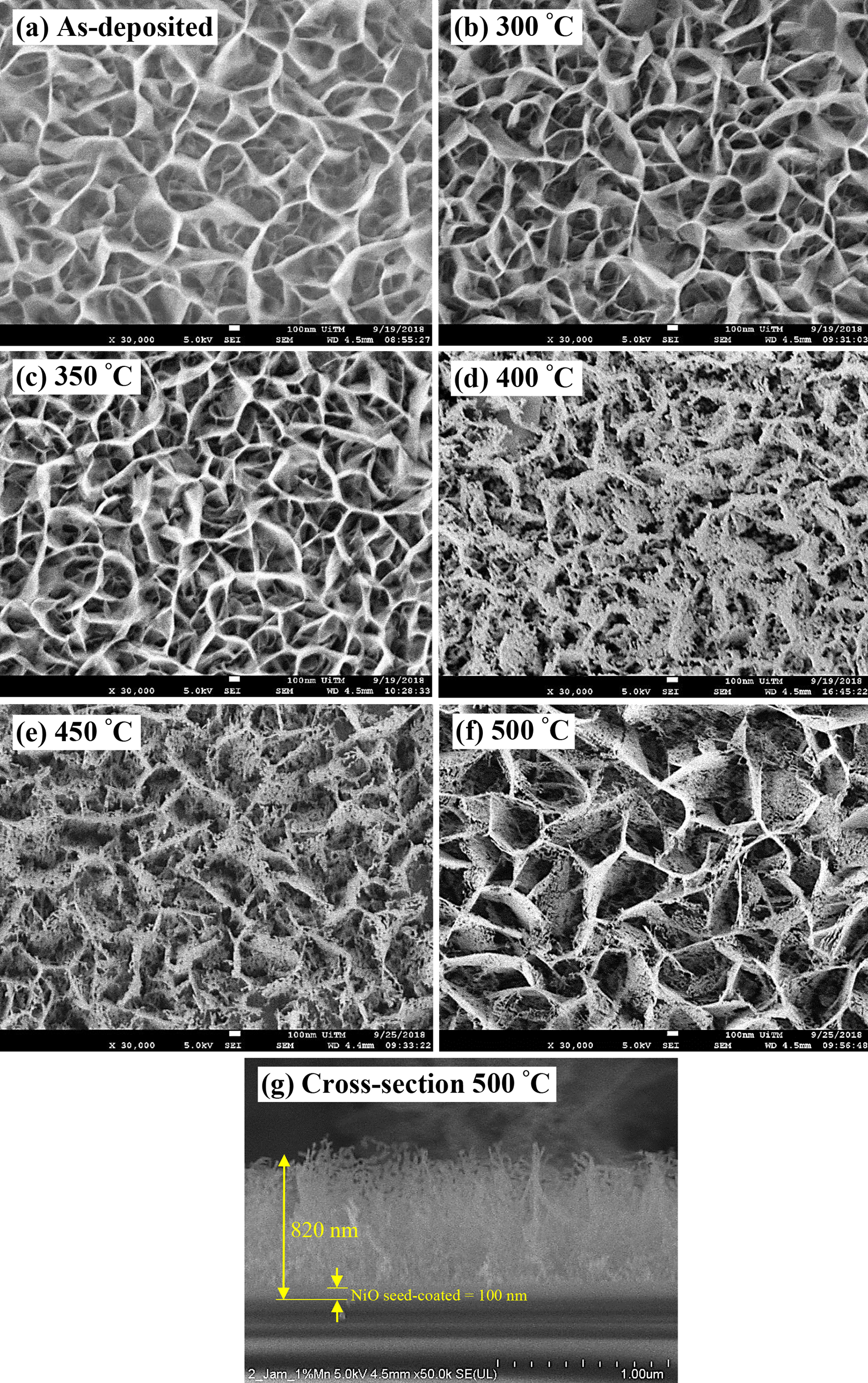
(a) to (f) Surface morphological images of as-deposited sample and annealed samples from 300°C to 500°C. (g) Cross-sectional image for Mn-doped NiO annealed at 500°C. Mn-doped NiO: manganese-doped nickel oxide.
The cross-sectional image of Mn-doped NiO annealed at 500°C, as shown in Figure 1(g), shows that the nanosheet structure was grown with a uniform distribution on the NiO seed-coated glass. From the cross-sectional point of view, a uniform nanosheet array with a hollow structure can be seen. The nanosheet thickness estimated from the FESEM image is approximately 820 nm and the seed-coated thickness itself is 100 nm. From the characterisation of the cross-sectional images, the thickness decreases as the annealing temperature increases. The nanosheet thicknesses are 1.0 μm, 950 nm, 900 nm, 880 nm, 850 nm and 820 nm for the as-deposited, 300°C, 350°C, 400°C, 450°C and 500°C samples, respectively. At higher annealing temperatures, the NiO nanosheets transform into a more ordered phase with reduced defects, whereby the atom rearrangement process occurs to achieve stability based on the supplied thermal energy. Subsequently, the thickness decreases due to dimensional shrinkage.
EDS was used to determine the elemental composition of the sample annealed at 500°C and the result is shown in Figure 2. The EDS analysis was conducted on top of the nanosheet surface and it confirmed the presence of Ni, O, C and Mn. There were no impurity elements detected in the EDS spectrum other than those described. The strong signals were due to O and Ni, which recorded fraction quantities of 49.01 and 46.51 at.%, respectively. In addition, the signal referred to C from the annealing process was at 3.48 at.%. Finally, Mn was detected at 1.01 at.%, which proved that the dopant was successfully included at 1 at.% in the NiO lattice. It is noteworthy that the elements from the glass substrate were not observed in the EDS analysis. A similar observation was reported by Wang et al. for a 300-nm-thick 2D NiO film on Ta glass substrate. 21

EDS spectrum with the atomic percentage of the Mn-doped NiO nanosheet array annealed at 500°C. EDS: energy dispersive X-ray spectroscopy; Mn-doped NiO: manganese-doped nickel oxide.
The Mn2+ ion has only a marginally smaller ionic radius of 0.67 Å than the Ni2+ ion (0.69 Å) in the same octahedral coordination. Therefore, Mn2+ is expected to occupy the Ni2+ site in the NiO matrix without significantly changing the crystal structure. 5,6 Furthermore, the appearance of a low concentration (1 at.%) of Mn2+ and the deficit of free carriers are believed to be the reasons for the absence of ferromagnetism behaviour. 17 A schematic model for the growth of the Mn-doped NiO nanosheet array film is depicted in Figure 3. The NiO nuclei on the NiO seed coating are formed when the supersaturation level in the solution exceeds its critical value. The dense nanosheet layer formed on the seed coating is caused by the homogenisation of the precursor ions and other reactants in the solution. 12

Schematic growth mechanism of Mn-doped NiO nanosheet array films on seed-coated glass substrate. Mn-doped NiO: manganese-doped nickel oxide.
Structural analysis
The XRD patterns in a 2θ range of 10–90° for the Mn-doped NiO nanosheet array films are shown in Figure 4. The XRD patterns exhibit different diffraction peaks for the as-deposited and annealed samples. For the as-deposited sample, as can be seen in Figure 4(a), the diffraction peaks at 2θ = 11.8°, 33.0° and 59.1° are characteristic of α-Ni(OH)2, corresponding to JCPDS No. 38-0715. These peaks were indexed to the (003), (101) and (110) planes, respectively. The broad peak between 20° and 40° corresponds to the glass substrate, as reported in the literature. 22,23 These results show that NiO did not exist in the as-deposited sample. The diffraction peaks for the as-deposited sample are weaker in intensity compared to the peaks of the annealed samples. This condition shows that the crystallinity of the as-deposited sample is poor and the formation of NiO is still unfinished. 9 For this non-annealed situation, it can be said that the sample exhibits antiferromagnetic behaviour due to the synthesis occurring below the Néel temperature of approximately 523 K. 7 The high background noise from the XRD pattern could be attributed to the low crystallinity properties and thickness of the samples. 24 –26

XRD patterns of (a) as-deposited Mn-doped NiO and for annealing at (b) 300°C, (c) 350°C, (d) 400°C, (e) 450°C and (f) 500°C. XRD: X-ray diffraction; Mn-doped NiO: manganese-doped nickel oxide.
Figure 4(b) to (f) shows the XRD patterns annealed at different temperatures. The diffraction peaks of 2θ identified for the annealed samples correspond to JCPDS No. 047-1049. The patterns suggest that the annealed samples exhibit cubic polycrystalline crystal structures. Three diffraction peaks were recorded at the (111), (200) and (220) planes for all annealed samples. The XRD patterns show an increase in intensity with increasing temperature. Broader XRD peaks were observed for annealing at 300°C and 350°C, but these peaks become narrower as the annealing temperature increases up to 500°C. This shows that the crystalline quality improved at higher temperatures. Furthermore, it can also be seen that the peak at the (200) plane shows the dominant intensity. Therefore, the calculation of the crystal parameters at the (200) plane orientation was performed and is summarised in Table 1. For the as-deposited sample, the (101) plane was chosen for the calculation of the crystal parameters. The crystal parameters recorded in Table 1 include the full width at half maximum, crystallite size (D), dislocation density (δ), interplanar spacing (d), lattice parameter (a), unit cell volume (V), strain (ε) and stress (σ). The smallest V was obtained for the as-deposited sample, while the largest V was recorded for the sample annealed at 300°C using equation (1). The V was slightly decreased for the samples at subsequent annealing temperatures.
Various crystal properties of as-deposited and annealed Mn-doped NiO samples for the (101) and (200) planes, respectively.

Mn-doped NiO: manganese-doped nickel oxide; FWHM: full width at half maximum.

The value of a can be calculated from the d value
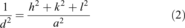
where

where n = 1 and h, k and l are the Miller indices of the selected plane. The 300°C sample exhibits the largest strain value due to it having the largest lattice parameter among the samples. The strain values at subsequent temperatures are found to remain constant. From the results, the negative strain (as-deposited) value means the strain is compressive strain, while positive strain (other temperatures) means the strain is tensile strain. The positive stress value by the as-deposited sample represented the tensile stress, while the negative stress value by other temperatures represented the compressive stress. 15,27,28
Table 2 shows the crystallite size calculated by the Scherrer equation for the Mn-doped NiO nanosheet arrays. Since the plane selected for the crystallite size calculation of the as-deposited sample was different from that of the annealed samples, the strain and stress values in Table 1 are clearly different. An overview of the trends in crystallite sizes for all the samples is illustrated in Figure 5. The crystallite size of the as-deposited sample was 1.3 nm and shrank to 0.63 nm when the sample was annealed at 300°C. The crystallite size was then gradually increased when the annealing temperature increased up to 500°C. The increase in crystallite size with increasing annealing temperature contrasts with the case of NiO films doped at different Mn concentrations. As discussed by Layek and Verma, the crystallite size decreases as the Mn dopant concentration increases. 6 The result also contradicts the study of undoped NiO by Chen et al., where it was reported that the crystallite size increases with increasing film thickness. 29 This result indicates that the annealing temperature plays an important role and has a significant impact on the crystallite size and other properties. However, Mn doping at 1 at.% did not alter the cubic structure and the lattice parameters of NiO in this study.
Total crystallite size of Mn-doped NiO nanosheet array films.
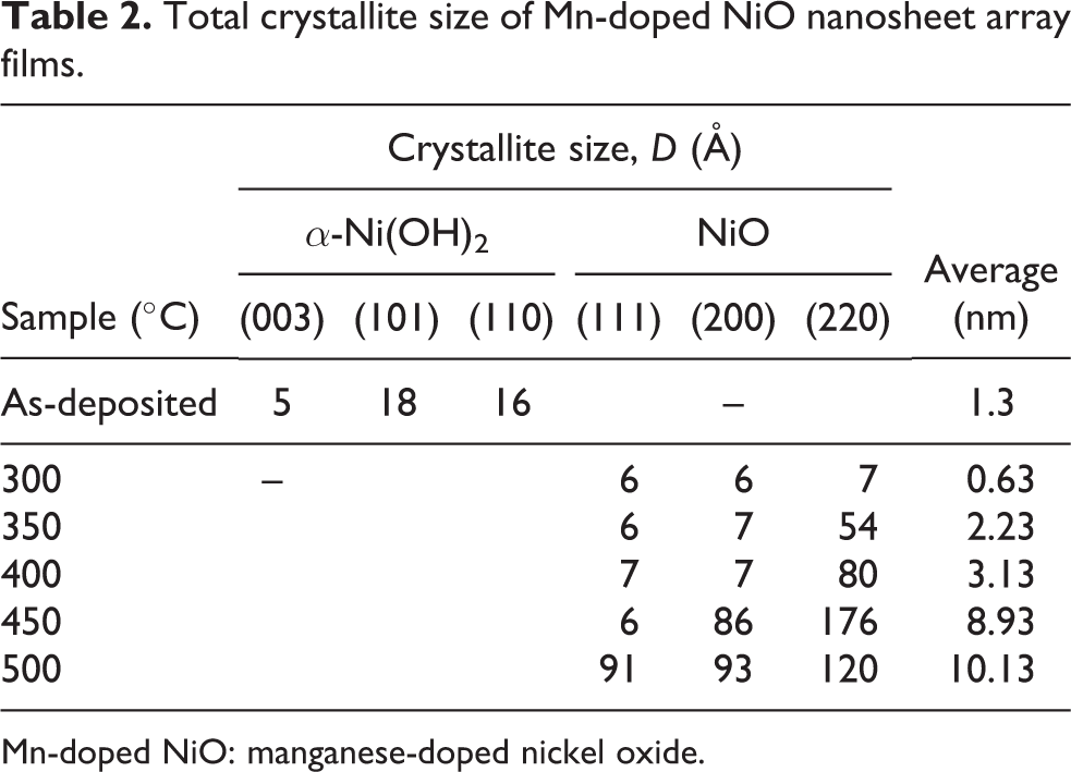
Mn-doped NiO: manganese-doped nickel oxide.

Total average crystallite size of Mn-doped NiO nanosheet arrays. Mn-doped NiO: manganese-doped nickel oxide.
Optical properties
The optical properties of the Mn-doped NiO nanosheet arrays at different annealing temperatures were investigated from the transmittance spectrum from UV–Vis spectrophotometry. The spectra in wavelength range of 300–800 nm for all the samples are presented in Figure 6. The highest average transmittance estimated from 400 nm to 800 nm was identified for the sample annealed at 500°C with a value of 50.7%, while the lowest was for the 300°C sample with a value of 13.7%. The trend in transmittance values from the as-deposited sample up to the sample annealed at 500°C is approximately the same with regard to the crystallite size in Figure 5. It can also be stated that the average transmittance of the samples increases with decreasing nanosheet thickness. The relation between thickness and transmittance is in line with the report by Meng et al. 30 In addition, Chen et al. reported low transmittance values from Ni2+ vacancies, which are the cause of hole conductivity. 29 The defect concentration and lattice imperfection decrease with increasing temperature, causing the transmittance value to increase.
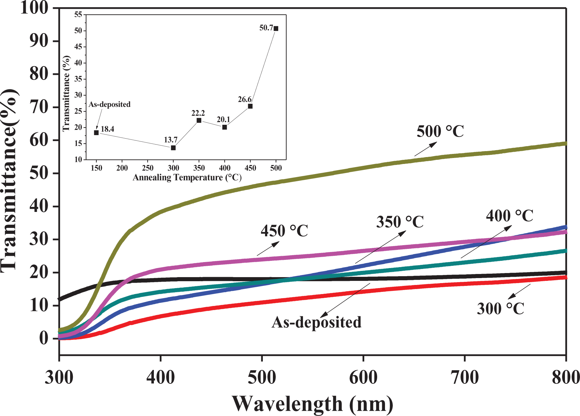
Transmittance spectra of Mn-doped NiO samples at different annealing temperatures. Mn-doped NiO: manganese-doped nickel oxide.
The optical band gap energies (E g) of the as-deposited and annealed samples are presented in Figure7(a) and (b), respectively. The E g was estimated by referring to a Tauc plot of (αhv) 2 versus photon energy (hv). Tauc’s relation is as follows

where α is the absorption coefficient, hv is the photon energy, B is an energy-independent constant (10 5 –10 6 cm−1 eV−1) that depends on electron–hole mobility and n = ½ and is used for a direct allowed transition. The E g value could be found by extrapolating the linear curve of this plot and using the hν value at the x-axis intercept. The E g values were estimated to be 3.85 eV, 3.51 eV, 3.66 eV, 3.50 eV, 3.63 eV and 3.60 eV for the as-deposited sample and the samples annealed at 300°C, 350°C, 400°C, 450°C and 500°C, respectively. This result shows that the heat treatment for the Mn-doped NiO strongly affects the optical band gap energies, resulting in the changeable band gap value. In addition, these results prove that the band gap is in the range of theoretical value of 3.6–4.0 eV. 31

Tauc plot of Mn-doped NiO for estimation of E g for (a) as-deposited and (b) annealed samples. Mn-doped NiO: manganese-doped nickel oxide; E g: band gap energy.
Electrical behaviour
To investigate the electrical behaviour of the heat-treated Mn-doped NiO, the I-V characteristics using a two-probe measurement system were determined at room temperature. The linear plots of I-V with a voltage range of −10–10 V, as shown in Figure 8(a), indicate the ohmic behaviour for all samples. The current that passes through the material is directly proportional to the voltage and complies with Ohm’s law. Based on the I-V measurement, the lowest resistance value of 3.69 MΩ is for annealing at 500°C, while the highest is for annealing at 300°C at 11.42 MΩ. The sample annealed at 300°C exhibits compressive stress (the most negative value), which contributes to the highest resistance of the sample. 32 With these results of resistance, the resistivity also follows the same tendency, while the conductivity was the opposite. In general, the conduction mechanism of the NiO films is determined mainly by the holes caused by Ni vacancies, oxygen interstitial atoms and the dopants used. 31 In this work, the electrical conductivity increases with increasing annealing temperature, which indicates that the contribution of Mn2+ can increase the carrier concentrations and mobility of the carriers at higher temperatures. Therefore, the sample at the highest annealing temperature (500°C) shows the highest conductivity value with 2.32 × 10⁻¹ S·cm−1. The relation between resistivity and conductivity is depicted in Figure 8(b). The values of resistance (R), resistivity (ρ) and conductivity (σ) of the samples are recorded in Table 3. From these outcomes, the doping of Mn at different annealing temperatures changes the presence of defects of NiO non-stoichiometry, hence altering the electrical performance.
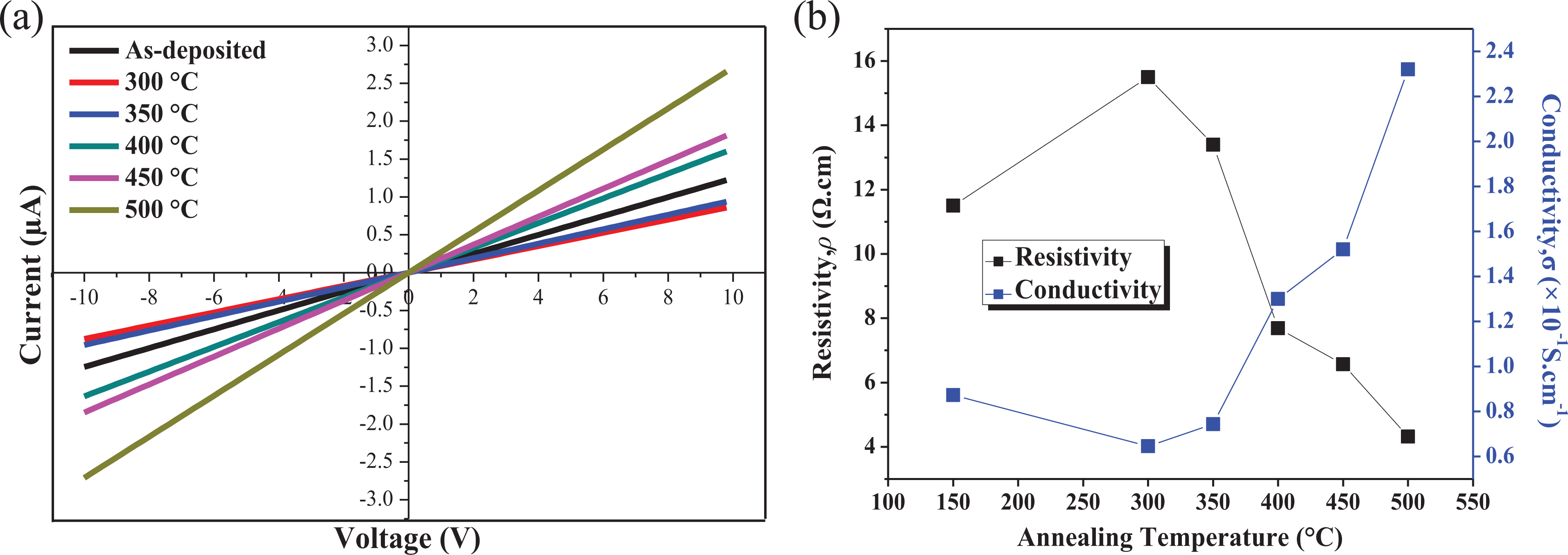
(a) I-V plots for resistance measurement and (b) resistivity and conductivity of Mn-doped NiO at different annealing temperatures. I-V: current–voltage; Mn-doped NiO: manganese-doped nickel oxide.
Resistance, resistivity and conductivity of Mn-doped NiO at different annealing temperatures.

Mn-doped NiO: manganese-doped nickel oxide.
Humidity sensor performance
During the measurement by the humidity sensor devices, Pt electrodes were used and the humidity chamber was set to 25°C with a voltage source of 5 V. The humidity levels of the chamber were also set between 40% and 90% relative humidity (RH). The changes in the current signal for one cycle of the Mn-doped NiO nanosheet arrays in humidity sensing performances at different annealing temperatures are shown in Figure 9(a). All the samples produced the same pattern of current responses with different heights. The sensitivity (S) of the sensor was calculated by dividing the current at the highest RH (I 90%RH) level to the current at initial RH (I 40%RH) level using the following equation

A summary of the sensitivity values at different annealing temperatures is presented in Figure 9(b). The sensitivity shows the curve of increment as the temperature increases with the highest sensitivity of 270 at 500°C, while the lowest is at 300°C with a sensitivity of 100. The highest sensitivity generated by a sample of 500°C may be attributed to the many factors from morphological, structural, optical and electrical properties caused by Mn doping. Among the main factors, it may be due to the presence of the high surface area-to-volume ratio with a high pore concentration that can excite water vapour diffusion and accelerates the adsorption of water molecules throughout sensing activities. 8 From the FESEM image in Figure 1(f), it is obvious that the sample annealed at 500°C possesses a larger surface area compared to others. In addition, the decrease in sensing performance also may be caused by the higher resistance due to the carrier scattering effect occurring at the grain boundaries. 33

(a) Humidity sensor responses of Mn-doped NiO nanosheet arrays with a bias voltage of 5 V and (b) summary of the sensitivity at different annealing temperatures. Mn-doped NiO: manganese-doped nickel oxide.
By comparing the same method and temperature from our previous work, 9 this highest sensitivity value has proved that Mn-doped NiO enhanced the sensitivity of the humidity sensor compared to undoped NiO (S = 257). The list of sensitivity values for each sample is shown in Table 4, together with the response (T r) and recovery (T c) times. The T r was measured during the adsorption process (calculated of 90% from 40 to 90%RH), while the T c was measured during the desorption process (calculated of 90% from 90 to 40%RH). The best T r and T c were produced by the sample annealed at 500°C with 359 s and 159 s, respectively, while the highest T r and T c were produced by the sample annealed at 400°C with 435 s and 231 s, respectively. Overall, it can be said that the T c is about half the T r for all the samples. As stated by Ismail et al., the highest T r and T c at a sample of 400°C can be explained by its higher density compared to other samples. This finding further showed that it has a lower porosity, which prevents water vapour access to the nanosheet structure. 32
Humidity sensing performance, including sensitivity, response time and recovery time of Mn-doped NiO at different annealing temperatures.

Mn-doped NiO: manganese-doped nickel oxide.
Figure 10(a) displays the stability behaviour of the Mn-doped NiO film annealed at 500°C. The film was measured and exposed to 40% and 90%RH for five cycles. The identical pattern with approximately the same height in the repeated reactions showed the sample stable for application as the humidity sensor. This shows the potential of the device for use in large-scale commercial applications. Figure 10(b) depicts the humidity sensing response of the 500°C Mn-doped NiO film at a different RH with five humidity levels ranging from 50% to 90%RH. The sensitivities of 50%, 60%, 70%, 80% and 90%RH are 1.9, 4.1, 12.1, 46.4 and 270, respectively. These results denote that the sample is sensitive to the different RH with the pattern of increment observed from these values.

(a) Repeatability responses of sample annealed at 500°C. (b) Humidity sensing responses of sample annealed at 500°C at different RH. RH: relative humidity.
Considering that NiO is a p-type semiconductor, the reported sensing mechanism is based on the formation of hole accumulation due to oxygen (O2) adsorption. 16 Furthermore, non-stoichiometric NiO is acknowledged as having a hole conductivity due to Ni2+ cationic vacancies and O2 interstitial defects. 34 A higher hole concentration is generated when higher Ni2+ cationic vacancies and Ni3+ ions (acceptor) are created in the film. 30 The presence of Ni3+ can provide a place for chemisorption of the hydroxyl groups during the sensing mechanism. 35
Generally, at low humidity levels with a small number of water molecules, the water molecules start to be adsorbed and chemically react on the nanosheet surface to form a chemisorbed monolayer. The attraction of water molecules was influenced by the electrostatic interaction between Ni3+ or Ni2+ and hydroxide ions (OH−). As the environment becomes more humid, another layer of the water molecule is physically adsorbed onto the chemisorbed monolayer. This circumstance is known as the physisorbed layer because of the formation of hydrogen bonds. The water molecules from the physisorbed layer were then decomposed into hydronium ion (H3O+) and hydroxide ion (OH−) because of the high electrostatic field on the top of the chemisorbed monolayer. Furthermore, H3O+ ions can be hydrated and produce a positive charge of (H+) ions. The positive charge (H+) from H3O+ jumps from one water molecule to another continuously and becomes the main charge carriers which are the source of electrical conduction. This hopping occurrence is called proton hopping, and the mechanism is known as the Grotthuss chain. Therefore, at this stage, more H+ ions will be generated and the increment in the current signal of the humidity sensor is caused by the protonic conduction. The reactions at the physisorbed layer can be expressed as follows 36 –38


At high humidity levels, the huge amounts of water molecules are adsorbed in the porous structure between the nanosheet arrays to induce capillary condensation. Simultaneously, electrolytic conduction occurs concurrently with the protonic conduction and achieves a state of equilibrium. During this stage, transportation charges increase outstandingly to produce the highest current signal. The high charge density area is also influenced by the presence of Mn2+, which provides an active surface centre to attract water adsorption, especially at higher temperatures.
Conclusion
Mn-doped NiO nanosheet arrays were successfully grown onto a NiO seed-coated glass substrate by employing two methods: sol–gel spin coating and an immersion method. The samples were distinguished by different post-annealing temperatures ranging from 300°C to 500°C to achieve an optimised NiO-based humidity sensor. The films grown produced different thicknesses and surface morphologies. XRD analysis revealed that the annealing temperature on Mn-doped NiO has a high impact on the crystallinity, as well as the crystallite size of the samples. The average crystallite size increased with increasing annealing temperature. In addition, the XRD patterns indicated that there were no impurity phases detected up to 500°C in the Mn-doped NiO samples. The optical band gap showed the decrement as the annealing temperature is increased. The conductivity showed improved performance as the annealing temperature is increased. The best performance of the humidity sensor is owned by a sample of 500°C with the sensitivity of 270. This sample also has the best response and recovery times at 359 s and 154 s, respectively. In conclusion, the incorporation of the Mn dopant at different annealing temperatures provided a simple method to determine and optimise the humidity sensor performance of the NiO nanostructures.
Footnotes
Acknowledgement
The authors thank the Faculty of Electrical Engineering, Universiti Teknologi MARA and Ministry of Higher Education, Malaysia, for their contribution and support to this research
Declaration of conflicting interests
The author(s) declared no potential conflicts of interest with respect to the research, authorship, and/or publication of this article.
Funding
The author(s) disclosed receipt of the following financial support for the research, authorship, and/or publication of this article: This research was funded by the Fundamental Research Grant Scheme (FRGS) (File No: FRGS/1/2018/TK04/UITM/02/23).