
Abstract
Two-dimensional transition metal dichalcogenides have gained great attention because of their peculiar physical properties that make them interesting for a wide range of applications. Lately, alloying between different transition metal dichalcogenides has been proposed as an approach to control two-dimensional phase stability and to obtain compounds with tailored characteristics. In this theoretical study, we predict the phase diagram and the electronic properties of Mo x Ti1−x S2 at varying stoichiometry and show how the material is metallic, when titanium is the predominant species, while it behaves as a p-doped semiconductor, when approaching pure MoS2 composition. Correspondingly, the thermodynamically most stable phase switches from the tetragonal to the hexagonal one. Further, we present an example which shows how the proposed alloys can be used to obtain new vertical two-dimensional heterostructures achieving effective electron/hole separation.
Introduction
The discovery of single-layer graphene 1 opened up the opportunity to realize innovative devices with outstanding performances such as field effects transistors (FETs) with unprecedented sensitivity. However, because of the lack of a bandgap, the applicability of graphene is limited. Recent research was devoted to find suitable two-dimensional (2D) alternatives such as hexagonal boron nitride, 2 black phosphorus, 3 graphene oxide, 4 silicene, 5 and transition metal dichalcogenides (TMDs). 6
TMDs are probably the most studied 2D compounds because of their tunable properties, which depend on their specific constituent elements and on their structure. The typical TMDs formula unit is MX2, where M represents a transition metal, while X corresponds to a chalcogen atom. Different M and X combinations offer a large pool of materials with wide range of properties which make them interesting building blocks for the realization of innovative sensors, 7 FETs, 8 solar cells, 9 light emitting diodes (LEDs), 10 and so on. Further, a given TMD can be usually found in distinct phases (polytypes) differing for the geometry of the metal coordination: a trigonal prismatic coordination (H-phase) and an octahedral one (T-phase). 11 Some TMDs are thermodynamically more stable in the H-phase while others are more stable in the T one; few compounds, such as MoS2, also exist in a distorted T-phase often referred as ZT or T′-phase. 11,12 Typically, changing the metal coordination modifies the hybridization of the d orbital involved in bonding with the chalcogen atoms and, consequently, it may alter the bandgap of the system 6 which, in many cases, passes from being metallic to semiconducting or vice versa. Different methods have been proposed to revert the phase stability of TMDs and, thus, control their electronic properties. For example, Rajesh Kappera et al. 13 have shown that lithium intercalation in multilayer MoS2 induces a permanent phase change from the stable semiconducting phase to the metastable metallic one leading to a decrease of the contact resistance in the devices. Reversible phase switching has also been achieved by hot electron injection into the 2D layer from plasmonic metal nanoparticles deposited on MoS2. 14 Another promising strategy, currently employed to engineer TMD monolayers, consists of alloying two different TMD compounds. 15 –17 Typically, it is either possible to substitute part of the metal atoms of a given MX2 with a different metal species (M′) which also exist in the form of a 2D structure (M′X2) to obtain M x M′1−x X2 alloys or it is possible to replace X with a different chalcogen atom (X′) to obtain MX x X′2−x . In limited cases, the possibility to vary both the metal and the chalcogen species has been explored. 18 For example, Pandey et al. have studied ordered mixtures of various TMDs 19 demonstrating the impact of alloying on the properties of the outcoming material, but in their study they restricted only to specific compositions. In another recent work, Raffone et al. 20 proved that combining density functional theory (DFT) simulations and cluster expansion (CE) calculations represent an effective way to predict the structural and electronic properties of TMD alloys in their full compositional range, and, in particular, they showed how a small addition of a substitutional metal atom is able to change the relative phase stability in MoS2.
In this article, we aim at studying the phase diagram and physical properties of novel alloys obtained by combining MoS2 and TiS2 employing the computational strategy presented by Raffone et al. 20 We have chosen to focus on MoS2 because several experimental studies proved that atomic layer deposition can be applied to growth monolayer MoS2 on conventional substrates, 21 followed by the deposition of another 2D materials to fabricate vertical heterostructures; 22 these may then be used in devices such as solar cells, LEDs, FETs, photodiodes, and sensors. TiS2 was instead chosen because it is characterized by a very small lattice mismatch with MoS2, thus this couple may originate alloys characterized by reduced strain and good thermodynamic stability. Moreover, since titanium (Ti) atoms have two d valence electrons less than MoS2, similar to niobium impurities, 23 it may originate p-type character structures and modify the intrinsic n-type character of MoS2. This would open up the way for the realization of sharp bilayer heterojunctions achieving efficient electron–hole separation, as proved by the example presented in the last part of the article.
Methods
The prediction of the structure, stability, and electronic properties of MoS2, TiS2, and their alloys has been carried out by combining DFT and CE. The CE simulations were performed by employing the ATAT, version 3.04 24 software, while for the DFT calculations we used the plane-wave approach as coded in the QUANTUM ESPRESSO, version 6.0 25 software package. The coupled CE-DFT approach is a well-established method that allows predicting with great accuracy alloy phase diagrams in their full composition range. 26 In particular, the phase diagram construction proceeds by following a step-by-step process involving alternating DFT simulations and CE predictions. The software implementing CE proposes an appropriate alloy structure as input to the DFT code and, at the end of the quantum simulation, the total energy is returned to the CE program. The DFT total energies are the basic elements used to obtain interaction coefficients among groups of atoms in the alloy, also referred as effective cluster interactions, which then determine the configurational energy of any structure at varying concentrations such that the most stable one is identified. In this way, the expansion is used to predict the energy of all configurations for the full concentration range, accessing also those arrangements that are computationally too demanding for DFT and preventing the need for an extremely large set of ab initio simulations. 27 This approach has been successfully applied to the prediction of other 2D TMD alloys. 20 Concerning the DFT methodology, the Perdew–Burke–Ernzerhof functional 28 was employed to account for exchange–correlation energy and the electron–ion interaction was described by ultrasoft pseudopotentials. A plane-wave energy cutoff of 50 Ry (500 Ry) for the wave functions (electron densities). The k-point grid was set to (8 × 8 × 1) for MoS2 and TiS2 monolayer primitive cells and reduced accordingly for supercell calculations, so to keep constant the density of the k-point mesh in the reciprocal space. A vacuum region of about 10 Å was introduced in the supercell in the direction perpendicular to the monolayer to avoid spurious interactions between periodic replicas; structure relaxation was assumed at convergence when the maximum component of the residual forces on the ions was smaller than 10−5 Ry/Bohr. In the case of the heterojunction, the minimum energy structure was obtained by applying the DFT-D2 correction to account for dispersive interactions between layers. 29 For each Mo x Ti1−x S2 alloy configuration, the formation energy, both for DFT and CE simulations, was calculated as follows

where
Results and discussion
As introduced earlier, MoS2 and TiS2 monolayers exist in different polytype structures, thus, before discussing their alloys, we here revise the relative stability, the structural and electronic properties of their pure phases as found at DFT level. In particular, MoS2 presets a stable H-phase which is semiconducting and a distorted metastable T-phase, usually called ZT or T′, which has a very small bandgap (see structures in Figure 1). The undistorted T-phase would be metallic, but it is unstable and spontaneously relaxes to ZT. For TiS2 on the contrary the most stable phase is T, which is reported to be metallic 30 or with a very small bandgap, the H-phase is metastable while the distorted ZT does not exist. The results of our simulations, summarized in Table 1, are in agreement with previously reported data 20,30,31 and confirm the picture described above. H-MoS2 has a bandgap of 1.58 eV which reduces to 0.06 eV in the ZT-phase in exact agreement with what reported by Raffone et al. 20 In the case of Ti, T-TiS2 has a very small bandgap of 0.05 eV (unlike Xu et al., 30 bands do not overlap), while for the H-phase the energy gap amounts to 0.73 eV. An analysis of the predicted equilibrium lattice parameters (see Table 1) reveals that the stable phases of the two compounds (H-MoS2 and T-TiS2) are characterized by a small lattice mismatch (about 6%). It could be, then, possible to obtain a stable alloy from these materials. Moreover the different electronic properties of the two compounds in their stable structure open up the possibility to tune the bandgap and other electronic properties in a wide range of values through alloying.
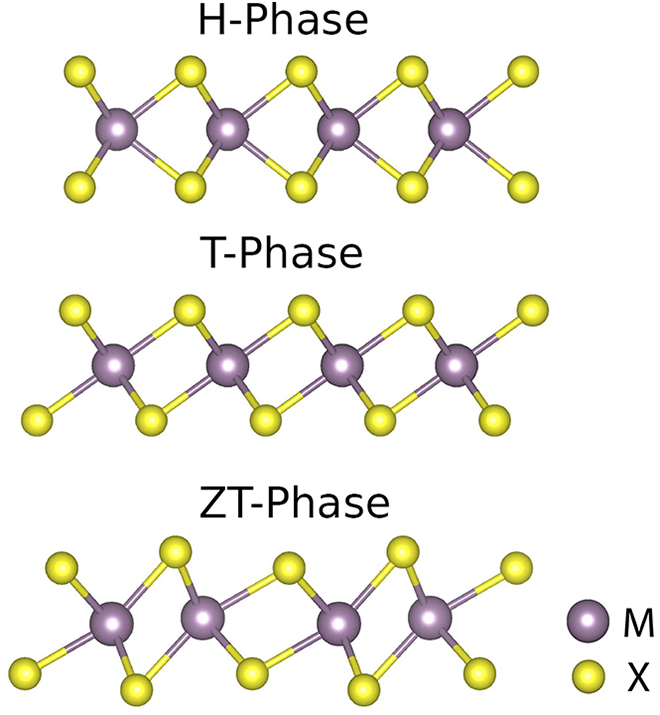
Balls and sticks representations of the three typical 2D-TMDs polytypes (H, T, and ZT phases). Yellow and violet spheres represent the chalcogen and metal atoms, respectively. TMD: transition metal dichalcogenide.
a and b, E g, and ΔE between the most stable phase (taken as zero of energy) and the least stable one for both TiS2 and MoS2 monolayers.
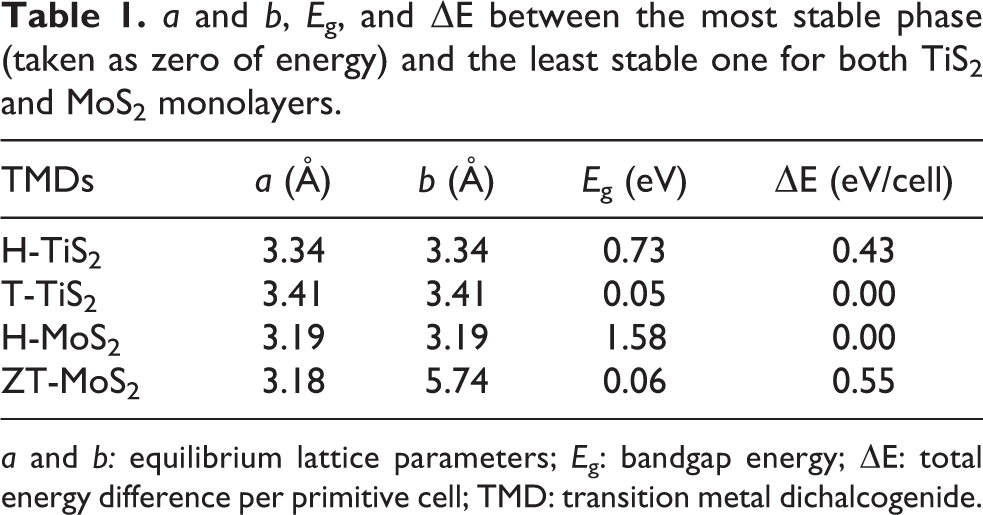
a and b: equilibrium lattice parameters; E g: bandgap energy; ΔE: total energy difference per primitive cell; TMD: transition metal dichalcogenide.
To obtain the phase diagram of Mo x Ti1−x S2, we computed separately the CE of the alloy in the H and ZT/T phases in the full range of x variability. The results of the formation energies as a function of the alloy composition are summarized in Figure 2, where the two reference energies are T-TiS2 total energy for x = 0 and H-MoS2 total energy for x = 1. The graph shows how the formation energy of the alloys in a given structure (H or T) varies with respect to these reference energies. In particular, the red and blue encircled dots (cross marks) represent the alloy energy calculated by means of DFT (CE) simulations for the H-phase and T-phase respectively. The values represented with crosses correspond to the CE configuration energies as obtained on the basis of the DFT results. Further, the solid lines in the plot represent the minimum energy structures throughout the whole x range and originate the so-called convex hull shape. The phase diagram clearly proves that as the concentration of Ti increases in MoS2 (x values close to 1 or smaller) the alloy formation energies increase for the H-phase but they decrease for the T-phase. On the contrary, as more Ti atoms in TiS2 are substituted with Mo atoms (x values close to zero or larger); the alloy formation energies increase for the T-phase but they decrease for the H-phase. It is apparent that a crossover between the two phases occurs at Mo concentration x = 0.45. Below this point the alloy is more stable in the T-phase: The Ti atoms are the majority metal species and thus the more stable structure of TiS2 is retained; for x x larger than 0.45, the H-phase becomes more stable as the Mo metal species becomes predominant. A similar behavior has been observed for Mo x Sn1−x S2 alloys in a previously published work. 20

Mo x Ti1−x S2 phase diagram showing the DFT calculated formation energies for the H (encircled blue dots) and T (encircled red dots) phases and the resulting predicted energies obtained from CE for the H (blue cross marks) and T (red cross marks) phases. The encircled green dot represents the DFT formation energy of a specific alloy composition Mo0.9375Ti0.0625S2 with H structure. DFT: density functional theory; CE: cluster expansion.
We now discuss, how the electronic properties of the lowest energy alloy structures change as a function of the composition. To this aim, we analyzed the density of states (DOS) and the bandgap of Mo x Ti1−x S2 along the convex hull line. All the compounds with x smaller than 0.45, retaining T structure typical of TiS2, appear to be metallic: None of them present an energy gap between the valence and conduction band. As an example representative of this stoichiometry range, we reported in Figure 3 the comparison between the DOS of the pure T-TiS2 and that of Mo0.33Ti0.67S2. It is apparent that the presence of Mo atoms in TiS2 increases the number of states at the Fermi level, which would correspond to an increase of the conductivity in the alloyed compounds with respect to pure TiS2.

Density of states of (a) TiS2 and (b) Mo0.33Ti0.67S2 in their lowest energy T structure. Dashed line corresponds to the Fermi level, taken as zero of energy.
The electronic features of Mo x Ti1−x S2 samples with x > 0.45 are summarized in Figure 4, where we show the DOS of four representative samples with an increasing amount of Ti atoms. It is evident that in the DOS of the sample with low Ti concentration (e.g. green circle of Figure 2) acceptor states appear right above the top of the valence band of the system if compared to the DOS of pure H-MoS2. Namely, Ti atoms, when substituting molybdenum, act as p-type dopants for H-MoS2, consistently with the fact that they have two less valence electrons in comparison to Mo. As the concentration of Ti increases, the number of acceptor states above the Fermi level increases; correspondingly their spread in energy is wider and the effective energy gap between the highest energy acceptor states and the conduction band minimum decreases, as clearly evident from Figure 4(a) to (d).
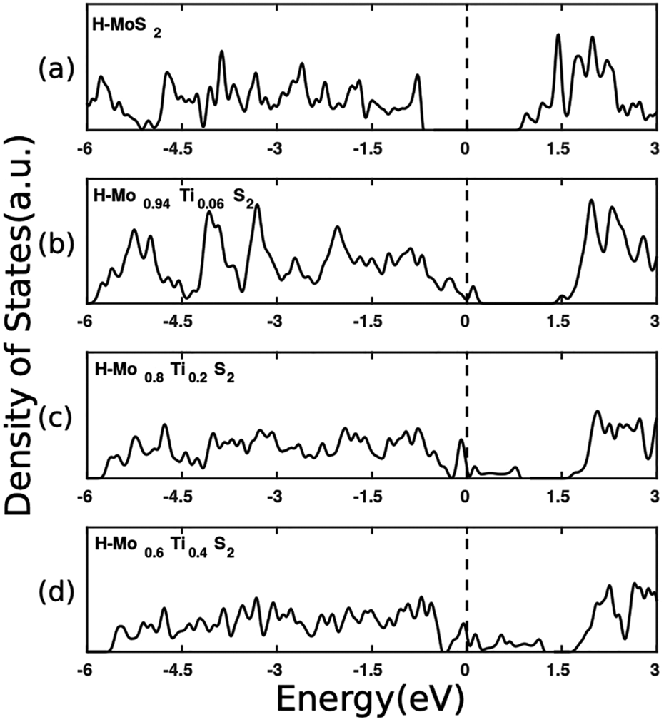
Density of states of (a) MoS2, (b) H-Mo0.9375Ti0.0625S2, (c) H-Mo0.8Ti0.2S2, and (d) H-Mo0.6Ti0.4S2 in their lowest energy H-structure. Dashed line corresponds to the Fermi level, taken as zero of energy.
Having found that Mo x Ti1−x S2 alloys with small amount of Ti are characterized by p polarity, we further investigated if these structures can be employed in 2D vertical heterostructures to effectively achieve electron–hole separation between the two layers. To this aim, we interfaced a low -energy p-type monolayer, such as the one represented by the encircled green dot in Figure 2, with an n-type structure. Recently, it has been shown that an effective way to obtain n-doped H-MoS2 consists of surface functionalization with organic moieties such as alkyl groups 32 or −H fragments; 33 these fragments generate shallow donor states and move the Fermi level of H-MoS2 close to the bottom of its conduction band. We thus built a bilayer system obtained by stacking H-Mo0.9375Ti0.0625S2 with H-MoS2 which adsorbed a –CH3 fragment and a hydrogen atom on its surface (see the structure reported in Figure 5).

Balls and sticks representation of the heterostructure obtained by stacking H-Mo0.9375Ti0.0625S2 (bottom layer) and an H-MoS2 which adsorbed a –CH3 fragment and a hydrogen atom (top layer). Yellow, violet, and cyan spheres represent S, Mo, and Ti atoms respectively. White and black spheres correspond to hydrogen and carbon species respectively. The blue (red) isosurface corresponds to electron charge accumulation (depletion) with respect to the isolated monolayers.
An analysis of the DOS projected on the n- and p-type monolayers reported in Figure 6 reveals that, when the junction is formed, the donor states of the –CH3 modified H-MoS2 layer are partially emptied and the electrons are transferred to the acceptors states of the H-Mo0.9375Ti0.0625S2, which become partially filled. Due to this partial filling, the Fermi level of the heterostructure raises if compared to the DOS of isolated H-Mo0.9375Ti0.0625S2 (see to the DOS reported in panel (b) of Figure 4). To highlight the charge transfer occurring at the heterojunction, we calculated the electron density difference between the interacting bilayer systems and isolated ones: The blue isosurface of Figure 5 represents charge accumulation, while the red isosurface represents charge depletion. It is apparent that most of the blue isosurface is localized in the bottom layer (p-type H-Mo0.9375Ti0.0625S2), while the largest part of the red isosurface is localized in the upper layer (n-type organic functionalized H-MoS2). Consistently with the picture gained by the PDOS analysis, a spontaneous charge transfer from the n- to the p-type layer of the heterostructure occurs that originates an effective electron–hole separation between the two layers. The entity of transferred charge has been qualitatively confirmed by calculating the sum of the Löwdin charges of each layer before and after the formation of the junction and amounts to 0.13 electrons/cell.
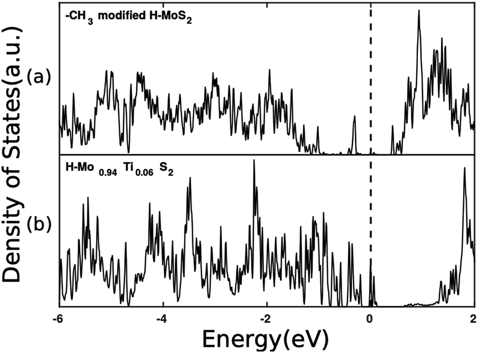
Density of states projected on the (a) functionalized H-MoS2 layer and on the (b) H-Mo0.9375Ti0.0625S2 layer of the heterostructure. Dashed line corresponds to the Fermi level, taken as zero of energy.
Conclusions
In summary, in this article, we have predicted the thermodynamic stability and the electronic properties of Mo x Ti1−x S2 monolayers in the full range of x variability. We have found that the alloys exist in the T-phase structure, typical of pure TiS2 monolayer, when the concentration of Mo, x, is smaller than 0.45, and that in this regime the monolayer has metallic character. On the contrary for x values larger than 0.45, the monolayer is more stable in the H-phase, the samples are semiconducting and show p-type polarity. With this respect, alloying H-MoS2 and T-TiS2 appears to be an effective approach to engineer the physical properties of these 2D structures. Lastly, we have proposed an example of application of our studied systems by realizing a vertical heterostructure composed of Mo x Ti1−x S2 (at low Ti concentration) and −CH3 functionalized H-MoS2. In this system, due to the p–n character of the junctions, electron/hole spatial separation between the two layers is achieved. We propose that such type of heterostructures could be employed in innovative nanostructured devices such as solar cells or sensors.
Footnotes
Acknowledgments
The authors acknowledge the CINECA award under the ISCRA initiative and HPC@POLITO, for the availability of high-performance computing resources and support.
Declaration of conflicting interests
The author(s) declared no potential conflicts of interest with respect to the research, authorship, and/or publication of this article.
Funding
The author(s) received no financial support for the research, authorship, and/or publication of this article.