
Abstract
MXenes have been under a lot of scientific investigation due to the novel characteristics that are inherent to two-dimensional nanostructures. There are a multitude of MXenes being studied and one of the most popular among these would be the titanium carbides. The general formula for titanium carbide is Ti n + 1C n for the nanosheets produced that have undergone much study in the past few years. These studies include how the etching process affects the final MXene sheet and how the post-processing via heat or combining with polymers and/or inorganic compounds influences the mechanical and electrical properties. It is found that different etching techniques can be used to change the electrical properties of the produced MXenes and different post-processing techniques can be used to further change the properties of the nanosheets. The possible application of the titanium carbide MXenes as chemical sensing and energy storage materials will be briefly discussed. MXene nanosheets show promise in such devices due to their high surface area to volume ratio and their specific surface structure with feasible surface functionalization.
Introduction
A large class of two-dimensional (2-D) transition metal carbides and nitrides have been under investigation for the past few years. These are materials that have a layered structure with (n + 1) layers of M (the early transition metal) connected by n layers of X (carbon or nitrogen) and have a general formula of Mn +1 Xn (n = 1–3). These materials are called MXenes. MXenes are made by atomic layers, and the thickness of a single stack of MXenes is about 1 nm. Different combinations of M and X can generate different compositions of MXenes, and there are reports that more than 20 different compositions of MXenes are synthesized, and over 70 different compositions of MXenes are theoretically predicted. 1 Such a wide range of compositions in MXenes provides an exciting playground for property tuning, and the understanding of process–structure–property relationships. Like other 2-D nanostructured materials, such as graphene, metal oxides, and boron nitride (BN), MXenes have a similar structure and electrical properties that could be an alternative to other 2-D materials in many cases and show promising properties for applications in gas sensing, energy storage devices, wearable electronics, and other high-performance energy applications. 2 –7
This review will focus on one of the more popular MXene materials discovered to date; titanium carbide MXenes, Tin+1Cn . They exhibit an unusual and unique property of metal-like conduction of heat and electricity and have mechanical properties of ceramics, such as being strong and brittle. These properties make them widely useful for energy and extreme temperature related applications. 8 –11 In this article, the synthesis of MXenes by exfoliation of the so-called MAX phases and forming titanium carbide MXene nanosheets through etching processes will be described and how such processes affect the structure and properties of Tin + 1Cn will be discussed. Further post-processing of these MXenes will also be explored to see how the electric and optical properties change and how these changes can be exploited for various applications.
Materials and methods
Titanium carbide MXenes are created from Ti n + 1AlC n powder; this is the MAX phase of titanium carbide MXenes. 12,13 This powder is made using TiC, Ti, Al, and activated carbon powders. The first step of making the MAX powder requires the precursors are put in correct molar amounts for desired molar values in the MAX phase and are then ball-milled in absolute alcohol for 24 h. Blended powders are then dried in a vacuum and sieved with a 100-mesh screen. These powders are then put in a flowing argon atmosphere, heated at a rate of 30°C min−1 to final temperatures of 1200–1500°C, and held for 15–60 min. Samples can be made in a range of 5–1000 g. 12 It was found that bulk MAX phase could be made using this method. The purity will not be influenced by the as-synthesized mass, final temperature, and holding time.
These synthesized powders can then be exfoliated by immersing them into hydrofluoric acid (HF) at room temperature. The solution can range from about 10% wt to 50% wt in HF concentration for varying amounts of time.
2,7
Figure 1 shows the basic schematic of this process, and the before and after of the etching can be seen in Figure 2. The process of etching is also the key step which creates functional groups attached to the surfaces of the MXenes. The basic reactions that occur to etch the MAX phase are as shown below


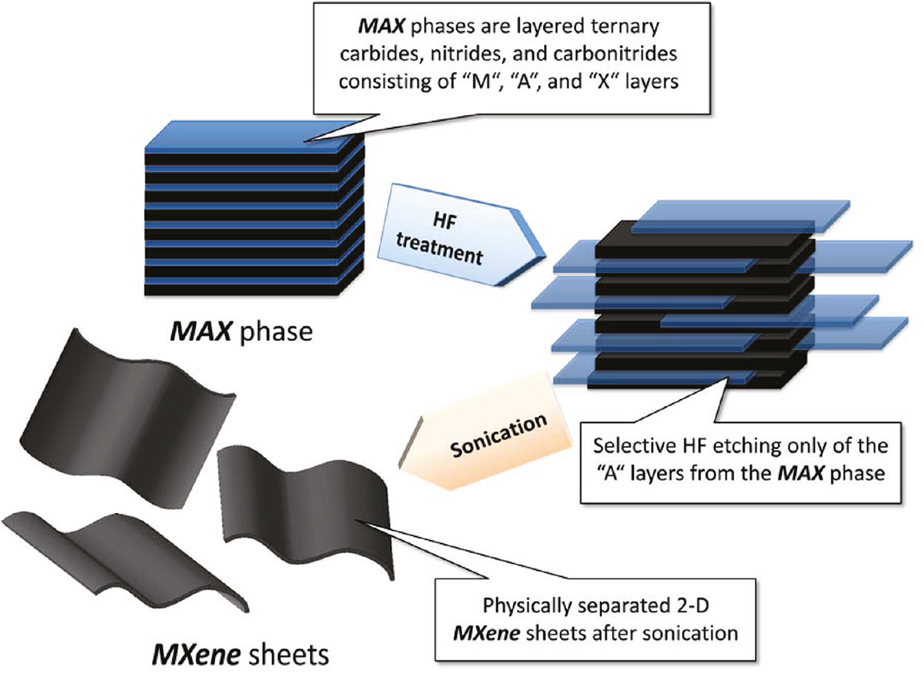
Basic map of etching process of the MAX phase to MXene nanosheets. Reproduced with permission from Naguib et al. 2

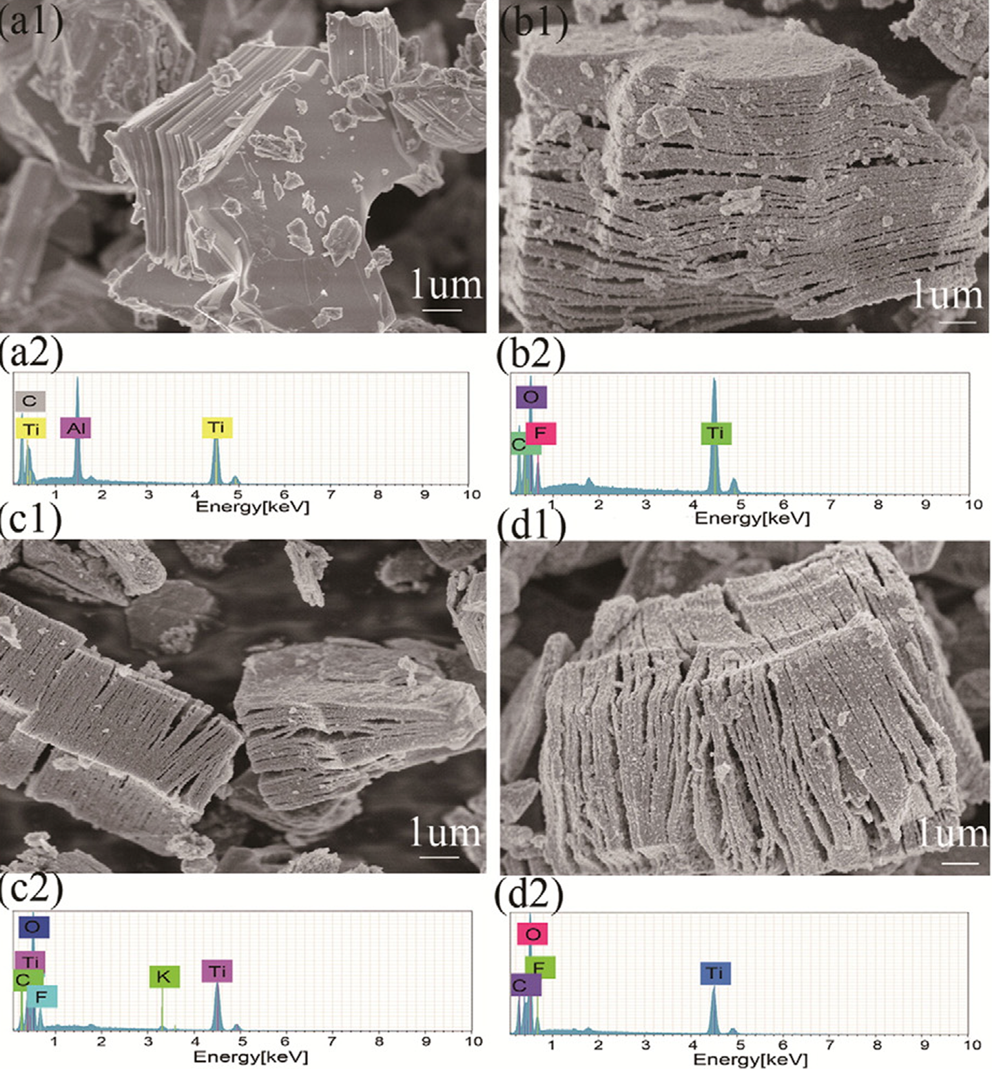
SEM images of (a) Ti3AlC2 MAX phase (b) Ti3C2 MXene. SEM: scanning electron microscopy. Reproduced with permission Naguib et al. 2
Reaction (1) is the etching step that removes the Al layer. Reactions (2) and (3) happen then simultaneously and cause the functionalization of the surface. Study has also gone into the etching of the MAX phase with bifluoride compounds (NaHF2, KHF2, NH4HF2) as well and how this affects the surface functionalization and spacing of the nanosheets. 12 The MXenes are then vacuum dried for about a day.
The as-synthesized MXene sheets can be terminated with different functional groups (=O, −OH, −F) following different etching procedures or post-processing. Such properties of MXenes can be directly used or designed for different applications. For example, some of the post-processing methods such as reinforcing the nanosheets with chitosan, 14 polyvinyl alcohol (PVA), 4 or polydiallyldimethylammonium chloride (PDDA) 4 can change mechanical and electrical properties of MXenes for applications in energy storage, supercapacitor electrodes, and sensors. In a word, etching and post-treatments of MXene sheets are critical procedures to change material properties for different application purposes. In the following sections, a detailed description about how etching and post-treatment can affect material properties of MXenes will be presented.
Discussion
Chemical treatments-based etching processing
The etching step is one of the most important parts of the process to form the MXene nanosheets, and many variables can be used to find how the etching affects the final material. HF is the most common etchant. As seen in Figures 3 and 4, the concentration of HF and etching time can significantly change the crystallinity and morphological properties of the resulting MXenes. 7 It was found that the etching rate using 40% HF solution took about 10 h at room temperature for Ti3AlC2 to remove the all Al layers out and form delaminated MXenes. This is an important step in MXene fabrication, because it gives information about how much surface area can be obtained over a certain period of etching time. This is especially useful for the applications in gas/chemical sensing devices that require larger surface area for better sensing performance. 15 –17


More study has also gone into different etchants and how these can change the material’s final properties. The X-ray diffraction (XRD) patterns, as shown in Figure 5, are of titanium carbide MXenes created with different bifluoride etchants and increasing etching times at 60°C. The different bifluorides used are NaHF2, KHF2, and NH3HF2. It can be seen that the 2-h and 4-h samples still mainly consisted of the MAX phase Ti3AlC2 when using NaHF2 etchant. When the etching time is increased to 8 h, the characteristic peak (39.2°) of the MAX phase significantly decreases. This indicates a critical time in the etching period needed to form layered MXene sheets. Similarly, the KHF2 etchant needed at least 8 h for a significant amount of nanosheets to be formed. NH4HF2 etchants only took 2 h to start forming a substantial amount of MXene nanosheets as seen by almost immediate disappearance of the characteristic peak. Figure 5 also reveals that two (002) peaks at 7.1° and 8.6° appear at the same time when using NH4HF2. This indicates that different layer spacing is formed simultaneously. However, when exfoliating up to 12 h, the 8.6° peak began to gradually decrease until it disappeared. This means a preferred interlayer spacing was formed after extended etching times. The scanning electron microscopy (SEM) and energy-dispersive spectroscopy (EDS) of the same samples can be seen in Figure 6. 12

XRD patterns of Ti3AlC2 etched in (a) NaHF2, (b) KHF2, and (c) NH4HF2 for varying times. XRD: X-ray diffraction. Reproduced with permission from Feng et al. 12
SEM (1) and EDS (2) of (a) Ti3AlC2 etched in (b) NaHF2, (c) KHF2, and (d) NH4HF2. SEM: scanning electron microscopy; EDS: energy dispersive microscopy. Reproduced with permission from Feng et al. 12
Above study has revealed that different etchants can be used to exfoliate the MAX phase and form Ti3C2 MXene nanosheets. One of the important findings is that using different fluorides to exfoliate can create different distances or spacing between sheets. This can be used to control the average interplanar spacing between sheets while fully exfoliating the MAX phase into MXene nanosheets. Another important finding is that different exfoliators can cause the produced MXenes to have different functional groups. 12 Further study should be done on how this could be exploited to customize the surface functional groups and specialize these materials for sensing applications.
Post-treatments
Since the etching process is usually conducted in an aqueous environment, it makes the as-obtained MXene sheets terminated with oxygen-containing and/or fluoride functional groups. 2,18 Post-treatments, such as using either alkalization to remove fluoride functional groups or calcination to remove the OH functional groups, can be used to change material’s surface properties. 19 However, the synthesizing processes include multiple steps with many pathways, and this makes the analysis of MXene surface functional groups very complicated. A technique was developed by Hope et al. to use H-1 and F-19 nuclear magnetic resonance to quantify surface functionalization from different pathways. This technique provides a simple method to analyze MXene functional groups. 20
In addition, through the methods of solution dispersion and electrospinning, it is common to use other materials with MXene nanosheets to create an MXene-based composite. This is another way to change MXene surface properties. For example, different polymers, such as chitosan, or Nafion can be used, to create composites. 14,21 Such MXene composites are very useful for applications in biosensors. For example, chitosan has been used to bind enzymes to the surface of MXene nanosheets for sensing organophosphorus pesticides (OPs) in water, and a similar method has also been used for the detection of phenol in water. 16,22 Therefore, using polymers to functionalize MXenes has a large impact on the possible sensing applications. There are quite a few different polymers used for this purpose. So, it is very important to plan carefully and fully understand the main purpose of the desired application when deciding which polymer is best for the application.
Other post-treatments can use inorganic compounds such as TiO2 and Au nanoparticles. Luo et al. synthesized TiO2/Ti3C2 MXene composites via hydrothermal growth followed by calcination to create a material with high photocatalytic activity. 23 By combining these two materials, they were able to increase the photocatalytic activity for the degradation of methylene blue. Au nanoparticles can be decorated onto Ti3C2 MXenes via chemical reduction method. 24 Au/MXene nanocomposites in this study show high sensitivity to blood glucose levels when glucose oxidase (GO x ) is immobilized on the surface using Nafion polymer. The Au decorating plays a significant role in the electron exchange between the GO x and the electrode. This means Au-decorated MXenes have a high potential for enzyme immobilized sensors because they allow for easy electron transfer between enzyme and MXene.
In a word, all of these post-treatment examples have revealed that using inorganic and organic compounds to modify the surface of MXenes can form different composite materials with broad applications.
Electric and optical properties
Many studies of the electrical properties of Ti3C2 MXenes have focused on the post-processing via thermal treatment of the material to modify the surface. 7,19 For example, it was found that alkalization in dilute NaOH followed by calcinating the MXene at 400°C and 600°C can increase the conductivity of MXene from 850 S cm−1 to 2410 S cm−1, respectively. However, further increasing the calcinating temperature above 600°C will cause the nanostructure to be collapsed. 19 Beside this, the electrical properties of MXenes can be manipulated using materials such as chitosan 14 and PVA. 3,4 Another study found that the resistance of the material will be increased when reinforcing MXenes with certain amount of chitosan. This can make the material almost unusable as electrical devices such as sensors. So, it is critical to use a correct ratio of chitosan to MXene when designing MXene-based biosensors that rely on enzyme immobilization. The increase of resistance with respect to percentage of weight in chitosan is shown in Figure 7. 14 In addition, study has indicated that MXenes can be combined with polymers such as PVA and PDDA to create stronger films, which can then be used as electrodes for supercapacitors. 3,4

Electrical resistivity versus chitosan content used to reinforce MXene sheets. Reproduced with permission from Hu et al. 14
Another study has taken an approach by sputtering the MAX phase onto a substrate and then exfoliating the A-layer using HF and NH4HF2 to investigate the transmittance of the material in hopes of furthering electronic, photonic, and sensing applications. 15 Table 1 shows the data obtained from these experiments. The film labeled IC is the film exfoliated with NH4HF2, and this film requires a much longer etching time. In every case, the film had the highest resistivity when it was thinnest. However, the IC sample did have the highest transmittance of all the samples when the film was thinnest, but the resistivity was a few magnitudes higher than the rest of the samples. These results show that MXenes have potential as transparent power sources, electrodes, and sensors. Utilizing MXenes fabricated in this fashion could lead to new transparent electronics. 25
Thickness, etching duration, resistivity, and light transmittance (wavelength = 700 nm) of the deposited and etched Ti3AlC2 thin Films.

Source: Reproduced with permission from Halim et al. 15
As for optical properties, MXenes can have high photothermal conversion efficiency with certain surface modification. For example, Liu et al. have been modifying the surface of MXenes to increase the optical property for application of anti-cancer therapies. 26 They have actually worked to inhibit the etching process so that the nanosheets hold onto some of the Al atoms. These Al atoms then react with the etching solution to create an Al oxyanion functional group. These obtained functionalized MXenes have a photothermal conversion efficiency of 58.3%. This new material is combined with anticancer drug doxorubicin and tumor-targeting hyaluronic acid to find tumors and aid in destroying them using the heat they produced when exposed to radiation.
Applications
Applications as sensing devices
Nanomaterials have become prominent in sensing applications due to their high surface area nature. This allows them to be very sensitive to chemical and physical changes. As a new family of two-dimensional (2-D) materials, MXenes indeed show promising surface properties for applications as sensor devices that can range in use from industry safety, environmental pollution, and public health care. For example, Ti3C2 MXenes have been modified with the enzyme acetylcholinesterase (AChE) and chitosan to create a nanocomposite-based biosensor for detecting organophosphate pesticides (OPs) in water. 16 These sensors have quite a low limit for detection at 0.3 × 10⁻¹⁴ M with a wide linear dynamic range. Such excellent sensing performance can give highly accurate readings on these toxic pesticides in water, and a sensor device using this material could test if residual OPs are on consumer food produce. Chitosan/MXene nanocomposites show promise for applications in sensors due to mix of chitosan’s high biocompatibility and MXenes’ high electrical conductivity. But, as shown earlier, the concentration of chitosan can cause the resistivity to raise too high to be used in electronics. To avoid this, using high concentration HF etching to immobilize enzymes in chitosan has proved to be an effective method of obtaining high surface area quickly without increasing the resistivity a lot.
Similar to the above sensing application, Ti3C2-based MXene can also be used to immobilize hemoglobin (Hb) as a mediator-free biosensor using Nafion/MXene composite. The results showed that MXenes-Ti3C2 is an excellent immobilization matrix with biocompatibility for proteins . 21,27 Due to the large surface area and high conductivity of MXenes-Ti3C2 with immobilized Hb, MXenes-Ti3C2-based biosensor displayed good performance for detecting nitrite ions with a wide linear range of detection from 0.5 µM to 11,800 µM and a very low detection limit of 0.12 µM. 21 This study further proves that MXenes can be used to immobilize proteins and create a protective microenvironment for the proteins to retain their activity and stability. In addition, Wu et al. immobilized tyrosinase on Ti3C2 MXenes as biosensors to detect phenol in water with the detection limit as low as 12 nmol L−1. 22 All these studies indicate that MXenes have high potential for enzyme immobilization, which can be used for highly effective biosensors.
Another promising application for MXene in sensors is in industry. Specifically, O-terminated MXenes can be used as ammonia (NH3) sensors. 17 A computational study based on O-terminated MXene nanosheet revealed that MXenes with this type of surface functional group are able to selectively and accurately detect NH3. The experiments conducted by Lee et al. further confirmed that Ti3C2T x MXenes can be used to detect common volatile organic chemicals such as acetone, ethanol, methanol, and ammonia. 28 In particular, if MXenes have been exfoliated by submerging the MAX phase in mixture of 9-M HCl and 1 g of LiF at 35°C for 24 h. The sensors they made had the highest response to ammonia and could be reliable used as ammonia sensors.
Applications for electrical storage
Currently, MXenes have also been successfully applied in electrochemical energy storage. This is because of their inherently high metallic conductivity and self-functionalized surfaces. Ti2C has been found to be a highly effective cathode host material for lithium sulfur (Li-S) batteries. 29 It is shown to have very stable cycling performance and a high capacity when using a 70% wt Sulfur/MXene composite. This composite has shown a decay rate of around 0.05% per cycle. This makes it competitive to other state-of-the-art materials used for sulfur battery technology that have a decay rate from 0.028% to 0.07% per cycle. Due to this composite’s very good cycling performance and low decay rate, it is a front runner as a Li-S battery cathode.
One of the most prominent applications for MXenes is as supercapacitors. MXene-Ti2C is found to have a gravimetric capacitance of 450 F g−1 at a scan rate of 1 mV s−1 and values even greater for Ti3C2. Overall, both Ti2C and Ti3C2 have a layered electrochemically active surface that can be used for high charge storage in capacitance applications. 8 However, a challenging factor for creating these MXenes as supercapacitor electrodes was the layered structure would collapse during fabrication. It was found that with added layers of reduced graphene oxide, MXene nanosheets were more robust during drying and electrode frabriation. 30 However, adding graphene can reduce the overall conductivity of the composite. The results are summarized in Table 2.
The effect of layering Ti3C2 MXenes with graphene on density and conductivity.
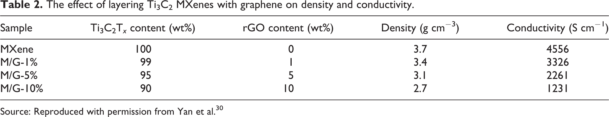
Source: Reproduced with permission from Yan et al. 30
Conclusion
In a word, due to the high surface area to volume ratio and specific surface structure with feasible surface functionalization, MXenes are proved to be a promising new 2-D nanomaterial with great potential applications in sensing devices and electrical storage. Today, many studies have indicated the same MAX phases can form different MXene nanosheets with variable material properties. This is due to utilizing different pathways such as exfoliation chemicals and post-treatments that affect the final material. This can change the conductivity of the bulk material. It is also revealed that the terminal groups of the nanosheets can be varied using different exfoliants during the fabrication processes. All these factors can be used to optimize MXenes properties for the applications in chemical sensing or electrical storage devices.
Footnotes
Declaration of conflicting interests
The author(s) declared no potential conflicts of interest with respect to the research, authorship, and/or publication of this article.
Funding
The author(s) disclosed receipt of following of financial support for the research, authorship, and/or publication of this article: This work is supported in part by the Offerdahl Seed Grant, NDSU Centennial Endowment Award, FAR0029296; and ND NASA EPSCoR research grant, FAR0030154, and ND EPSCoR seed award, FAR0030452. We also wish to acknowledge the NDSU Core Research Facilities for providing access to microfabrication tools and materials characterization instruments.