
Abstract
A template/electrochemical deposition method for fabricating silver nanorod arrays based on porous anodic alumina was presented. The barrier layer of porous anodic alumina templates was thinned by step-by-step voltage decrement method. Subsequently, silver ions were reduced into the channels of porous anodic alumina templates by electrochemical deposition method. Electrochemical impedance spectroscopy was utilized for analyzing the thickness of barrier layer of porous anodic alumina templates; the elementary composition and the size of silver nanorod arrays were characterized by X-ray diffraction and field-emission scanning electron microscope, respectively. Experimental results showed that the thickness of barrier layer of porous anodic alumina was suitable for alternating current electrochemical deposition, when anodizing potential was decreased to 70 V and widening time of porous anodic alumina in H3PO4 solution is 80 min. And the silver particles could be deposited into the channels of porous anodic alumina templates at 11 V, 13 V, and 15 V. Different sizes of silver nanorod arrays were obtained by controlling the deposition time. The average diameter of silver nanorod is in the range from 346 nm to 351 nm which is almost consistent with the pore diameter of porous anodic alumina templates (367 nm). The uniform silver nanorod arrays have a considerable potential in the flexible and wearable electronic devices, optics, solar cell, the catalytical electrode, and so on.
Keywords
Introduction
Recently, noble metal nanomaterials, especially 1-D nanostructures, have been a major direction in materials science because of their unique electrical, catalytic, optical, magnetic, excellent mechanical properties and outstanding effect such as small size effect, interface effect, quantum dimension effect and macroscopical quantum tunnel effect. 1 –4 Many researchers have focused on fabrication of 1-D different shape noble metal nanostructures such as nanowire, nanorod, nanosphere, nanocube, and shape-controllable nanostructure. 5 –8 Silver nanostructures with excellent electrical and thermal conductivity, optical property, biocompatibility, antibacterial property, and large specific surface area were applied in many fields, 9 –12 such as wearable electronic devices, 13 liquid crystal display, 14 solar cell, 15 strain sensing, 16 gas sensing, 17 biological sensing, 18 optics, 19 surface-enhanced Raman scattering, 20 and the catalytical electrode 21 and others.
Usually, synthesis methods of silver nanostructure are composed of chemical and physical categories including polyol method, 22 solvothermal method, 23 ultraviolet irradiation method, 24 photoreduction method, 25 electrochemical method, 26 porous material template method, 27 –30 and wet chemical method. 31 However, wet chemical method has many disadvantages like requiring organic solvents, reaction atmosphere, heating, stirring, injecting, and different varieties of additives such as inorganic anions and metal cations. Compared with the chemical methods, the physical methods require special conditions like high temperature and pressure. Above-mentioned disadvantages have been overcome by electrochemical deposition with template-assisted in which nanostructures can be directly deposited into channels. It has many advantages: one-step, quick, environment friendly, low cost, and easy control morphology. At present, direct current (DC), alternating current (AC), and pulse current are widely used in electrochemical deposition. However, it is complicated and time-consuming for the DC electrochemical deposition to remove the barrier layer. And the high potential and current are employed in the process of pulse electrochemical deposition. In this article, uniform silver nanorod arrays are prepared by AC electrochemical deposition with porous anodic alumina (PAA) template-assisted. The barrier layer is thinned by decreasing voltage stepwise. This method is fast, efficient, and simple. The effects of deposition voltage and deposition time on the morphology are investigated.
In this study, the PAA templates with thin barrier layer will be produced by step-by-step voltage decrement method and be utilized for fabricating regularity silver nanorod arrays. Subsequently, the PAA templates and silver nanorod arrays will be characterized by electrochemical impedance spectroscopy (EIS), field-emission scanning electron microscope (FE-SEM), and X-ray diffraction (XRD). The uniform silver nanorod arrays have a good application prospect in the flexible and wearable electronic devices, optics, solar cell, the catalytical electrode, and so on.
Experimental and characterization
The fabrication procedure of silver nanorod was shown in Figure 1. Ordered PAA templates were prepared by an improved two-step anodization method in our previous work. 32 After the second anodization for 60 min, the anodizing potential would be decreased from 195 V to 70 V at the rate of 2 V/min for thinning the barrier layer. Then, in order to widen the hole and thin the barrier layer further, PAA templates were immersed in 5 wt% H3PO4 solution at 30 °C for 80 min. Subsequently, the PAA template and platinum electrode were, respectively, regarded as the work electrode and the counter electrode, and immersed into 3 g/L AgNO3 and 16 g/L H2SO4 mixture solution for 5 min to ensure the electrolyte into the channels of PAA template, electrochemical deposition was performed under 13 V alternating voltage AC potential for 15 min. To be convenient to characterize the silver nanorod arrays, the 25 wt% PMMA (polymethyl methacrylate)/DMF (N,N dimethylformamide) mixture solution was spin-coated onto the top surface of PAA template after the electrodeposition. 33 Then, the PAA template with silver/PMMA nanorod arrays would be heated in the drying oven for 60 min at 140 °C. Subsequently, the aluminum substrate was removed in a mixture solution of 0.1 M copper chloride and 10 wt% hydrogen chloride. Finally, 5 wt% phosphoric acid solution was employed to dissolve the PAA templates and release the silver nanorod arrays. All of the chemical reagents employed in this experiment are analytical grade.

Fabrication procedure of silver nanorod arrays/PMMA composite (green: Al, black: PAA, gray: silver, blue: PMMA). PMMA: polymethyl methacrylate.
The EIS was utilized for characterizing the thickness of PAA templates by POT/GAL 15 V–10 A electrochemical workstation (Novocontrolcompany, Germany). The morphology of PAA and silver nanorod arrays was characterized using an FE-SEM (Hitachi S-4800, Japan and MERLIN Compact, ZEISS, Germany).The chemical composition of silver nanorod arrays was measured by energy-dispersive X-ray spectroscopy (EDS; APOLLO XL, EDAX, Mahwah, NJ, USA). The XRD pattern was performed by a RigakuUltima IV (from Rigaku Corporation, Japan) with recording it in the 2θ range 5–90°. The diameter and length of the silver nanorod arrays were measured by IMAGEJ [version 2.1.4.7] software.
Results and discussion
The bode plot of PAA templates whose voltage decreased from 195 V to 70 V, 80 V, 90 V, respectively, with step-by-step voltage decrement is shown in Figure 2. At high frequency section (105–101 Hz), the value of EIS of PAA fabricated by 70 V, 80 V, 90 V minimum voltage, respectively, has a little distinction and are approximate 12,500 Ω. Then, the value of EIS increases gradually with the decreasing frequency. Especially, the value of EIS of PAA templates fabricated by the 90 V minimum voltage increased sharply and was more than 75,000 Ω. However, the value of EIS of PAA templates fabricated by 70 V and 80 V minimum voltage was less than 30,000 Ω. Meanwhile, with the frequency further decreased (101∼10−1), the value of EIS of the PAA templates fabricated by 70 V minimum voltage had fallen to 5000 Ω. It demonstrates that the barrier layer which is nonelectrical conductive has been thinned by step-by-step voltage decrement effectively. The thickness of the barrier layer is the essential factor of the AC electrochemical deposition. When the barrier layer is thick, the voltage is not enough to penetrate it to make the silver ions deposit. On the contrary, when the barrier layer is thin, the voltage can break down and destroy it. In this experiment, at first, PAA templates are processed by step-by-step voltage decrement from 190 V to 70 V. Subsequently, in order to thin the barrier layer and widen the diameter of holes further, PAA templates were immersed in 5 wt% H3PO4 solution for 80 min. And it also ensures that the silver ions would be deposited into the holes of PAA templates.

The bode plot of different barrier layers decreased from 195 V to 70 V, 80 V, and 90 V.
Figure 3(a) to (d) shows the SEM cross section images of silver nanorod/PAA formed with different deposition voltages from 11 V to 19 V. All the samples are deposited for 20 min. An amount of silver nanorod can be observed in the channels of PAA templates using the 11 V, 13 V, and 15 V deposition voltage as shown in the Figure 3(a) to (c). However, only a little of silver particles could be found in the channels of PAA templates using the 17 V and 19 V deposition voltage. Because the reduction potential of silver ions is higher than the hydrogen ions, hydrogen will be separated out during the whole deposition process. Obviously, when the thickness of barrier layer is constant, hydrogen evolution reaction will be more intense because of the increasing deposition voltage. Hydrogen evolution reaction and high deposition voltage can all destroy the barrier layer. The current trend of different deposition voltages at the beginning of the deposition process is shown in Figure 4. The current value of the deposition voltage of 11 V increases slowly from the beginning, and then it is close to the current value of the deposition voltage of 13 V and 15 V gradually. The reason is that the silver nanorod could be only found in the channels of PAA templates using 11 V, 13 V, and 15 V deposition voltage. However, when the deposition voltage is 17 V or 19 V, the current value will be large enough to break down the barrier layer at the outset. Hence, high anodizing voltage is not in favor of silver nanorod deposition for AC deposition approach. Additionally, the deposition process is very slow for 11 V deposition voltage which is accompanied with a little bubble. For 13 V or 15 V deposition voltage, the process of deposition is very quick and the color of PAA templates fleetly change from semitransparent to yellow and finally into black. Moreover, Figure 3(b) and (c) shows that some of the silver particles covered on the face and bottom of PAA templates due to rectifying properties vanished and the barrier layer destroyed by hydrogen evolution reaction. The silver ions are barely reduced to silver particles in the whole deposition process accompanying with lots of bubbles occurring for 17 V or 19 V deposition voltage. Only a little of silver particles in the channels of PAA templates could be observed as shown in the Figure 3(d) and (e). The reason is that the barrier layer of PAA templates is destroyed severely by the major deposition voltage and intense hydrogen evolution reaction.
The cross section SEM images of silver nanorod fabricated using (a) 11 V, (b)13 V, (c)15 V, (d)17 V, and (e)19 V deposition voltages for 20 min. SEM: scanning electron microscope.

The curves of the current versus time at different deposition voltages.
Figure 5 shows that the chemical composition of silver nanorod arrays based on PMMA substrate is characterized using energy-dispersive X-ray spectroscopy (EDS). The red region in the left of Figure 5 is surface scanning district of EDS. And the weight (wt) and atom (at) percentage of various elements is shown in the right of Figure 5. The weight percentage of silver is 44.7% and the atom percentage of silver is 86.8%. It demonstrates that the red region in the left is silver nanorod arrays which all stand upright on the PMMA polymer. Moreover, only 1.1 wt% and 2.2 at% aluminum as shown in table can prove that the PAA templates are removed effectively.

EDS of silver nanorod arrays. EDS: energy-dispersive X-ray spectroscopy.
The XRD pattern of silver nanorod arrays which are prepared under 13 V deposition voltage for 15 min is shown in Figure 6. The pattern shows that silver nanorod arrays have four peaks and the crystal signals of four peaks are located at diffraction angles 2θ = 38° (111), 2θ = 44.2° (200), 2θ = 64.3° (220), 2θ = 77.3° (311). The face-centered cubic silver can be identified by comparing the diffraction peaks with the standard XRD spectrum (JCPDS card 04-0783). The analytical results of XRD pattern validate further the test of EDS and also prove that silver nanorod arrays can be successfully prepared using AC electrochemical deposition.

XRD pattern of silver nanorod arrays. XRD: X-ray diffraction.
In general, silver can be deposited in the channel of PAA using AC, the reason is accounted as rectification characteristic of Schottky barrier in Al/Al2O3 interface, the Schottky barrier causes between Al and Al2O3 barrier layer is due to oxygen vacancy of single ion in Al2O3 barrier layer. Al and Al2O3 barrier layer can be regarded as a p-type semiconductor; hence, the valve effect can promote the reduction reaction of the silver ion on the silver ion solution and Al2O3 barrier layer interface when AC was loaded. However, new Schottky barrier appears between silver nanorod and Al2O3 barrier layer which is opposite to that of Al/Al2O3 interface. Meanwhile, the Schottky barrier of silver/Al2O3 interface increases with increasing length of silver nanorod, and the reduction reaction of the silver ion on the silver ion solution and silver nanorod interface ceases when the Schottky barrier of silver/Al2O3 interface is equal to that of Al/Al2O3 interface.
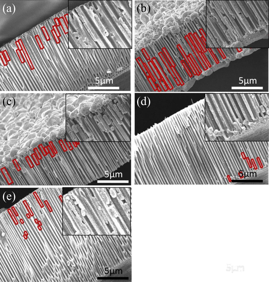
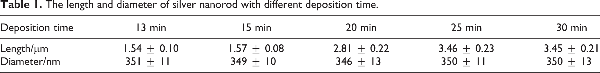
Figure 7(a) and (b) shows the cross section and surface SEM images of silver nanorod arrays which are processed under 13 V deposition voltage for 13 min deposition time. One can observe that the silver nanorod arrays contact with PMMA effectively. Therefore, the upright status of silver nanorod arrays is exposed and could be measured in the SEM images. However, the surface of silver nanorod arrays is not smooth and has apparent graininess. The reason is that the growth process of silver nanorod arrays is not continuous. And the silver ions are reduced to silver particles only at the negative part of AC. The length and diameter of different deposition time are shown in Table 1. The silver particles in the channels of PAA templates will increase gradually with the deposition time increasing. So the length of silver nanorod will also be added and grow to 1.54–3.45 μm averagely. Moreover, due to the silver nanorod growing restrictedly in the channels of PAA templates, the diameter of silver nanorod will not be changed apparently. The average diameter of silver nanorod ranges from 346 nm to 351 nm which is almost consistent with the pore diameter of PAA templates (367 nm). According to Figure 8, the deposition time has no influence on the diameter of silver nanorod. And the length of silver nanorod has no trend to be added sequentially after the deposition time gets to 25 min. It is the reason that the rectifying properties of the surface of Ag/Al2O3 is offset to the surface of Al/Al2O3 and the whole assemblies also do not show the rectifying properties at the process of AC electrochemical deposition. Thus, at this moment, prolonging the deposition time cannot increase the volume of silver particles in the channels of PAA templates.

(a) The cross section and (b) surface SEM images of silver nanorod fabricated under 13 V deposition voltage for 13 min with different deposition time. SEM: scanning electron microscope.
The length and diameter of silver nanorod with different deposition time.
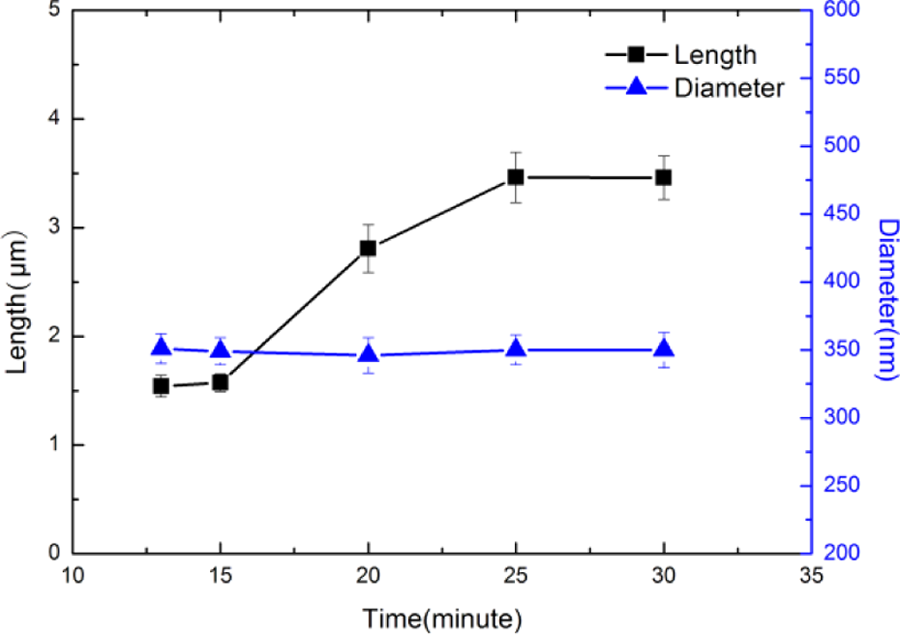
The curves of the length and diameter of silver nanorod versus deposition time.
Conclusion
In this study, an environmental, convenient, PAA template-assisted process has been successfully developed to prepare uniform silver nanorod arrays using AC electrochemical deposition. We found that the anodization voltage decreased stepwise from 195 V to 70 V can thin the barrier effectively. Through spin-coating the mixture solution of PMMA/DMF, the silver nanorod arrays could be obtained successfully. Deposition potential, one of the essential factors, determines whether the process of electrochemical deposition is feasible or not. The silver particles could be deposited into the channels of PAA templates at 11 V, 13 V, or 15 V. But, in contrast with 13 V and 15 V, the process of electrochemical deposition would be slower at 11 V. Different sizes of the silver nanorod arrays were prepared by controlling the deposition time. The average length is from 1.54 μm to 3.45 μm and the average diameter is 350 nm. This method for creating uniform silver nanorod arrays can have a wide variety of applications such as the flexible and wearable electronic devices, optics, 34,35 solar cell, 36,37 the catalytical electrode, 38 and so on.
Footnotes
Acknowledgments
The authors would like to express their gratitude to Dr. M. Hu for her valuable support. They also express their sincere thanks to Dr. N. P. Deng and Miss W. Li for their technical support.
Declaration of conflicting interests
The author(s) declared no potential conflicts of interest with respect to the research, authorship, and/or publication of this article.
Funding
The author(s) disclosed receipt of the following financial support for the research, authorship and/or publication of this article: The authors received financial form the National Natural Science Foundation of China (Grant No. 51473122, 61401417) and Postdoctoral Science Foundation of China (Grant No. 2016M591390) for support of the work reported in this article.