
Abstract
In this work, the pressure-sensitive properties of pure multi-walled carbon nanotubes and multi-walled carbon nanotubes/bismuth sulfide composite are investigated and compared. Composite was prepared by 50 wt% of each ingredient. Sandwich-type pressure-sensitive pellets (Ag
Introduction
In recent years, nanomaterials and its composites have drawn a great deal of interest in a wide range of applications, due to their enhanced chemical, electrical, physical, mechanical, optical, and biological properties. 1,2 Nanomaterials can be engineered through controlled and size selective synthesis techniques to tune its properties for a specific application. 3 This unique behavior of nanostructured materials and its composites lead to the current advancement in the field of nanotechnology, which opened the door to investigate its pressure-sensitive properties. Carbon nanotubes (CNTs) and bismuth sulfide (Bi2S3) are the promising nanostructured materials to be utilized in the field of sensing technology. 4,5 CNTs are 6 times lighter than steel, while its tensile strength is 60 GPa, that is 100 times higher than that of steel. The elasticity of the CNTs is almost 1 TPa, which is five times larger than that of steel. 6 The exceptional properties of CNTs such as high flexibility, low weight, and high gauge factor make them an ideal candidate for sensing technology. 5
On the other hand, there has been an intensive interest in fabrication and characterization of Bi2S3 and its composites due to potential suitability and exceptional technological importance of these materials.
7
Bi2S3 is a promising direct band gap (1.3–1.7 eV) orthorhombic structured n-type semiconductor nanomaterial.
8
At T = 300 K, its carrier mobility (μn
), carrier concentration (n), the range of electrical conductivity (σ), and refractive indices are 200 cm2V−1 s−1, 3.1018 cm−3, 10−7 to 10 Ω−1cm−1, and 1.3–1.9, respectively.
9
The direct band gap of Bi2S3 can be tuned by varying the shape and size of nanoparticles that result in different electrical, thermal, mechanical, and optical properties.
4,8
In view of the mentioned outstanding properties of both the CNTs and Bi2S3, we fabricated and characterized pure CNTs and CNT
An appreciable amount of research work on this topic can be found in the available literature.
5,6,10
–14
Recently, Hasan et al. demonstrated multi-walled carbon nanotubes/polydimethylsiloxane (MWCNT/PDMS) composite piezoresistive pressure sensors. For all types of MWCNT
Bi2S3-based field-effect transistor was fabricated by Park et al.
15
The electrical characteristics of the nanowire transistor were investigated by swapping the gate bias from 30 to −30 V and from −30 to 30 V again. The materials of the transistor was found to be n-type semiconductors and the observed on
The band gap energy of Bi2S3 is in the range of 1.3–1.7 eV, which lies in the spectra of the visible range. Therefore, the main focus of the researchers and scientists has been on to investigate the electrical, thermal, and optical properties of Bi2S3 and its composites. 8,17 –22 However, little effort has been extended to study the piezoresistive properties of CNT/Bi2S3 composites till date. We believe that the true potentials lie in the electromechanical and piezoresistive properites of the CNT/Bi2S3 composites that can be fully investigated.
The combination of these materials can share the benefits of the outstanding features of both CNTs and Bi2S3 that may have a good impact on the sensitivity and piezoresistive properties of the sensors. From a practical point of view, it will be useful for the future generation of sensors, actuators, and other electronic devices to deepen the knowledge about squeezing effect, physical, piezoresistive, and electromechanical properties of the CNT/Bi2S3 composites. In this article, for the first time, we reported the fabrication and characterization of a novel sandwich-type, pressure-sensitive sensor based on CNTs
Materials and experimental setup
Materials
The CNT nanopowder was commercially purchased from Sun Nanotech Co, Ltd, China. According to the supplier, length, outer diameter, and purity of the used MWCNTs were in the range of 1–10 μm, 10–35 nm, and >90%, respectively. The CNTs nanopowder was utilized without further purification. The nanostructured Bi2S3 nanopowder was kindly provided by Ahmad. 23 According to Ahmad, 23 Bi2S3 nanorods were synthesized by solid state reaction technique at ambient pressure and low temperature. The diameter and length range of Bi2S3 nanorods were approximately 20 nm and 100–150 nm, respectively.
Sample preparation
The materials were accurately weighed by digital weighing machine to measure the amount of the materials. A blend of Bi2S3 (50 wt%) and CNT (50 wt%) was prepared by carefully mixing the materials in an agate mortar and pestle (Applied Physics Thermal Lab", COMSATS Institute of Information Technology, Islamabad, Pakistan). The blend of the material is then poured from the top into a thick walled stainless steel cylinder with an inner diameter of 15 mm, closed at the bottom with a stainless steel movable piston. The top of the cylinder was closed by a well-fitted stainless steel plunger that is allowed to move down in the cylinder as shown in Figure 1. The diameters of both the pistons were 14.9 mm.

Schematic of thick walled stainless steel cylinder, movable stainless steel piston for closing bottom of the cylinder, and a well fitted stainless steel plunger to close the top of the cylinder.
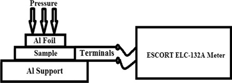
To make the pellets, the composite was pressed by hydraulic press at a pressure of 1000 PSI (6894.8 kNm−1) that results the sample to be more durable. The pressed tablet with thickness 2 mm and diameter 15 mm was ejected from the cylinder and both sides of the pellet were painted with silver (Ag) paste to provide low resistance electrical contacts. The top and bottom of the sample were covered with aluminum foils to avoid scratching of the sample due to external applied pressure. The schematic view of the sandwich-type pressure-sensitive sensor with the applied pressure is shown in Figure 2. Ag paste is a part of the sample and not indicated in the figure.

Schematic view of the pressure-sensitive sensor with applied pressure.
Setup and measurements
To investigate the pressure-sensitive properties of the materials, the sample was installed in experimental setup as shown in Figure 3.

Experimental setup for the characterization of pressure-sensitive properties with installed sensor.
The corresponding schematized concept of the experimental setup of Figure 3 for the characterization of the pressure-sensitive sensor is shown in Figure 4.
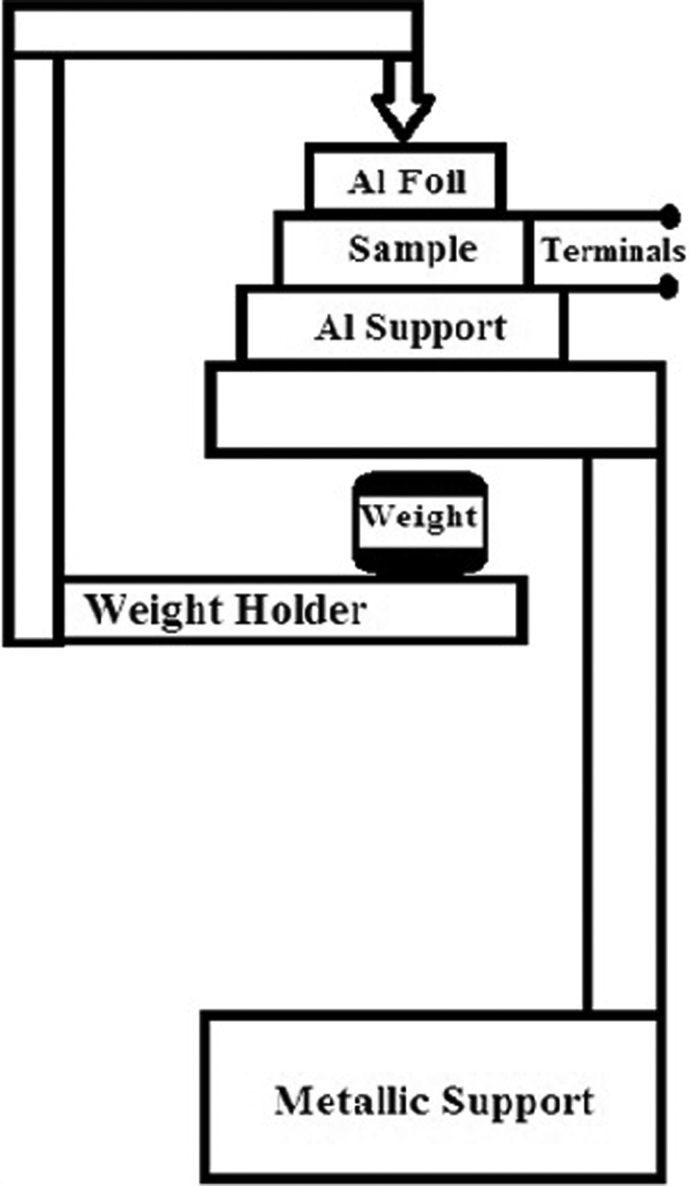
Experimental setup for the characterization of pressure-sensitive properties with installed sensor under pressure; composed of metallic support, weight, weight holder, aluminum support, sample, and aluminum foils as terminals.
Both sides of the prepared sample were covered with aluminum foils. The purpose of the aluminum foils was to act as leads of the sample and to protect the sample from scuffing as well. The sample with aluminum foils was placed on Al support as shown in Figures 3 and 4. The leads (aluminum foils) of the sample were connected to the test clips of the ESCORT ELC-132A meter (Applied Physics Thermal Lab", COMSATS Institute of Information Technology, Islamabad, Pakistan). The pressure value was changed by variation in values of the weights, holding by the weight holder as shown in Figures 3 and 4. The change in the direct current (DC) resistance of the sample with the variation in the external applied uniaxial pressure was measured from display readings of ESCORT ELC-132A meter as shown in Figure 5.
Schematic view of the sample with external uniaxial applied pressure connected with ESCORT ELC-132A meter to measure its DC resistance. DC: direct current.
The range, accuracy, and resolution of measuring instrument were 20 Ω to 10 MΩ, ± (0.5% rdg + 3 dgts) and 0.001 Ω to 0.001 MΩ. The weight and weight holder are the prime parts of the setup that were utilized from the traditional laboratory setup, Flexor (Cantilever flexure frame, Faculty of Mechanical Engineering, GIK Institute of Engineering Sciences and Technology, Topi, Pakistan).
Results and discussion
The surface morphology of the prepared samples was examined by scanning electron microscope (SEM, model: JSM5910; energy: 30 KV; magnification (max): 300,000×; resolution power (max): 2.3 nm; manufacturer: JEOL, Japan). The microscopic images of the surface morphology of pure CNT, pure Bi2S3, and CNT/Bi2S3 composite-based samples are shown in Figure 6. The SEM images of the all the three samples are presented with the same magnification.

SEM images of (a) CNTs-based sample, (b) Bi2S3-based sample, and (c) CNT
The surface of the CNTs-based sample (Figure 6(a)) seems to be a conductive network of the CNTs ropes. The porosity and rope size of the CNTs is not uniform. CNTs are the stiffest nanostructure materials but have the capability to bend. 24 Besides straight CNTs, somewhat curved nanotubes can be seen in Figure 6(a). Some of the CNTs are even bended to circular shapes. Such behavior of strong bending shows the extreme flexibility of MWCNTs, which makes these materials suitable for sensing technology. The MWCNTs utilized in this work has length from 1 nm to10 nm and diameter from 10 nm to 35 nm, respectively, as shown in Figure 6(a). SEM image of CNTs-based sample shows high aspect ratio up to 1000.
It can be seen from Figure 6(b) that Bi2S3 nanoparticles have no particular orientation. Probably, the formation of shorter Bi2S3 rods like structure occurs at the expense of longer rod-shaped nanoparticles. Various methods such as microwave irradiation, evaporation approach, solid state reaction, solvothermal/hydrothermal process, thermal decomposition, and direct reaction of sulfur and bismuth at high temperature in quartz vessel can be used to synthesis different size and morphology of Bi2S3 nanoparticles, to tune its band gap to fulfill the requirement of a specific device. 4 The synthesis of quantum size materials is also possible in some cases. 23 Solid-state reaction technique provides comparatively large size nanostructured Bi2S3 materials. The free fracture surface of the sample shown in Figure 6(b) depicts relative large size Bi2S3 nanoparticles with length from approximately 100 nm to approximately 150 nm and diameter of approximately 20 nm, respectively. The nanostructured Bi2S3 material utilized in this work was synthesized by solid-state reaction technique as mentioned in section “Materials.” Ranjbar et al. 25 observed a decrease in the energy band gap with increase in particle size of nanostructured Bi2S3 material. The reason for the selection of large size Bi2S3 nanostructured material synthesized by solid-state reaction technique was to reduce energy band gap (equation (6)) and to make the sample more responsive to the external applied pressure.
The microscopic surface morphology of CNT/Bi2S3 composite-based sample is given in Figure 6(c). The microscopic observations of CNT
It is quite clear from Figure 6(a) and (b) that the mergence among the nanoparticles within CNT and Bi2S3 samples is comparatively more than CNT/Bi2S3 composite-based sample (Figure 6(c)). In other words, the net interfacial distance between the nanoparticles within CNT and Bi2S3 samples (Figure 6(a) and (b)) is less than the interfacial distance between the nanoparticles within CNT/Bi2S3 composite-based sample (Figure 6(c)). Smaller interfacial distance between nanoparticles causes less porosity and more compactness of the material. Furthermore, smaller porosity in the materials makes the materials less responsive to external stimuli (pressure in our case). We can see in Figure 10 that CNT/Bi2S3 composite sample is more responsive than pure CNT-based sample, which supports our statement.
The pressure–resistance relationship for one of the Ag/CNT/Ag pressure-sensitive sensors at increase and decrease of the pressure is shown in Figure 8. A decrease in resistance was observed with increase in the applied uniaxial external pressure, called negative resistance coefficient.
It can be seen from Figure 7 that the resistance of the sensor is decreased from 5600 Ω to 1.3 Ω as the uniaxial applied pressure is increased from 0 kNm−2 to 16. 9 kNm−2. This shows a 4000 times (99.8%) decrease in the DC resistance of the sample.
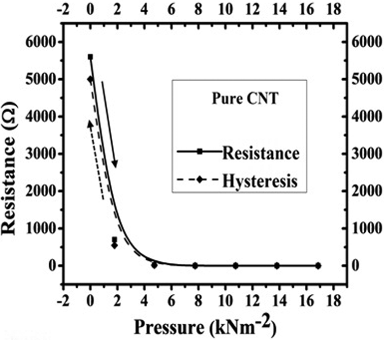
Pressure–resistance relationship for Ag/CNT/Ag sample at increase and decrease of the pressure. CNT: carbon nantotube; Ag: sliver.
The sensitivity (S) of the sensor was computed by equation (1) 10

Where ΔR, Ro
, and ΔP represent the resistance change, initial resistance (at P = 0 kNm−2), and the external applied pressure variation, respectively. The sensitivity of the CNT-based pressure-sensitive sensor in average was equal to 0.05 m2 kN−1. Higher pressure is required to compress and deform the thicker sample. This leads to a smaller variation in the sample resistance at a larger external applied pressure. Similarly, the nanoparticles in the sample, fabricated at a higher pressure, are in close contact with each other and have more conductive paths, eliminated pores among grain boundaries
The pressure–resistance relationship and hysteresis effect for CNT-Bi2S3 composite is shown in Figure 8. It can be seen from Figure 8 that, when the external uniaxial applied pressure ranging from 0 kNm−2 to 16.9 kNm−2 is applied on the sensor element, 4307 times (99.9%) decrease in the DC resistance is observed. The measured sensitivity for Ag/CNT-Bi2S3/Ag composite pressure-sensitive sensor was 0.06 m2 kN−1.

Pressure–resistance relationship for Ag/CNT-Bi2S3/Ag sample at increase and decrease of the pressure. CNT: carbon nantotube; Ag: sliver; Bi2S3: bismuth sulfide.
The decrease in resistance from 12000 Ω to 3 Ω is due to the large deformation produced in the sample by external applied pressure, which results in the formation of continuous conductive networks in the composite.
The resistivity was decreased sharply in the pressure range from 0 kNm−2 to around 8 kNm−2, beyond which the sample showed a negligible change in resistance. The reason is, when the external uniaxial applied pressure reaches to a certain value, called percolation threshold, beyond which the contact area between the nanoparticles in the composite hardly changes and no more new creation of the conductive paths occurs within the material of the composite. 11 The conductivity of Ag/CNT-Bi2S3/Ag composite got saturated above the percolation value (here, 8 kNm−2). The percolation value depends on different factors such as material type, processing, aspect ratio, and alignment, and so on. 27
The sensor’s resistance can be computed by equation(2). 28

Where d is the thickness or inter-electrode distance, ρ is the resistivity (ρ = 1 σ −1, where σ is the conductivity), and A is the cross-section (Al foil in our case) of the pressed tablet.
The change in resistance (see equation (2)) of the composite material can be influenced by two factors: (1) intrinsic property (resistivity) and (2) geometrical properties (length of the inter-electrode distance and cross-sectional area of the sample). In most of the nano and semiconductor material, the former case is dominated, because, most of the resistivity changes occur due to the variation of the charges concentration. Change in the resistance due to geometrical aspects is very small (a few %) as compared to the change in resistivity (99.9%) of the materials. Therefore, we considered the effect of intrinsic properties of the material in this case (see Figures 8 and 9).

Pressure–resistance relationships; simulated (dashed blue) from equation (4) and experimental (solid black) from Ag/CNT-Bi2S3/Ag composite sensor shown in Figure 8. CNT: carbon nantotube; Ag: sliver; Bi2S3: bismuth sulfide.
As CNTs and Bi2S3 are nanopowders. Therefore, decrease in resistance with the increase in pressure shown in pressure–resistance relationship (see Figures 9 and 10) may be due to (1) the reduction in the inter-electrode distance “d” of the sample by squeezing effect that decreases the distance between CNTs and Bi2S3 particles and (2) the traps between the highest occupied molecular orbital (HOMO) and lower unoccupied molecular orbital (LUMO) band gap in disordered material that may cause a potential barrier (trap states) to trap the charge carriers. The lower energy, highest filled π orbital is referred to as HOMO, while the first energy level just above the HOMO state is the higher energy or excited state of π-orbital denoted as π* called LUMO. The range of the gap between HOMO and LUMO is 1–4ev. 29,30 The localized energy states that exist between HOMO and LUMO levels are termed as traps. 31 The concentrations of the charge carriers may increase by densification effect of the nanoparticles of the material under the external applied uniaxial pressure. This increase in the concentrations may fill the trap regions in the material, which causes to increase the conductivity and hence decrease the resistance of the device. 32

Comparison of CNT-Bi2S3 composite sandwich-type, pressure-sensitive sensor with pure CNT-based sample; pure CNT (black solid line) and CNT-Bi2S3 composite (blue solid line). CNT: carbon nanotubes; Bi2S3: bismuth sulfide.
Equation 3 can be used to simulate the experimental results shown in pressure–resistance relationship (see Figure 9). 33

In our case, equation (3) can be written as

Where, R and Ro are the resistance under pressure P and the initial resistance at atmospheric pressure (0 kNm−2), respectively. Here, a = 11961.2 m2 kN−1, b = 0.5 m2 kN−1, and c = 38.8 m2 kN−1.
The simulated (see equation 4) and experimental results (see Figure 8) are in good agreement with each other as shown in Figure 9. Only 1.03% deviation of the experimental result from the simulated results were observed in this case.
The comparative pressure–resistance relationship for the CNT-Bi2S3 composite and pure CNT-based pressure-sensitive sensors is shown in Figure 10.
Here, the pressure-sensitive properties of CNT-Bi2S3 composite-based sample are compared with a press-tablet fabricated from pure CNT nanopowder. The sensitivity (0.06 m2 kN−1) of CNT-Bi2S3 composite-based sandwich-type pressure was found to be 1.2 times more than the sensitivity (0.05 m2 kN−1) of pure CNT-based sample. The decrease in resistance of CNT-Bi2S3 composite-based sample is 1.07 times higher than the resistance decrease of the pure CNT-based sandwich-type pressure-sensitive sensor. A decrease in the resistance with increase in the external applied uniaxial pressure from 0 kNm−2 to 16.9 kNm−2 is observed in both the samples. However, the effect of external applied uniaxial pressure on CNT/Bi2S3 composite is more significant than the effect on pure CNT-based sample. It can be seen from Figure 10 that, as the pressure increased, the CNT/Bi2S3 composite pressure-sensitive sensor exhibited a more disruptive slope than the sample based on pure CNT, especially in the pressure range from 0.6 kNm−2 to 4.5 kNm−2. The dimensions of the Bi2S3 nanoparticles (length approximately 100–150 nm, diameter approximately 20 nm) is smaller than the dimensions of the carbon nanotubes (length approximately 1–10 μm, diameter approximately10 –35 nm). When the particles size was decreased, the surface area-to-mass or surface area-to-volume ratio was increased and therefore, the reactivity (response to external stimuli) of the materials was increased.
2
In our case, we can assume that Bi2S3 (50 wt%) makes the CNT/Bi2S3 composite more uniform, which has a small amount of contaminations, porosity, dislocations, impurities, and other defects as compared to pure CNT-based sample.
34
Therefore, it may be one of the reasons that the resistance decrease in CNT
Atoms in the materials start vibrations when the temperature is higher than absolute zero. These vibrating atoms generate phonons (acoustic waves) that can act as a particle. Higher the temperature, more will be the phonons and vice versa. The phonon collides with charge carriers, which tend to increase the resistance of the materials. 35
On the other hand, dislocations (crystallographic faults) and other defects in the materials act as scattering centers for charge carriers. 35 The term scattering means the collision of free charge carriers with the dislocations and other defects in the materials. In scattering mechanism, the charge carriers interact (scatters) with the dislocations and other defects in the materials, which causes to decrease the mobility, and hence increases the resistance of the materials. 35 The mobility in a multicrystalline materials decrease or increase with the variation in temperature, but in fact, it depends on contribution of the scattering mechanism. 36
In most of the multicrystalline disordered system, hopping phenomenon of conduction was realized, in which the carriers are hoping out from one localized state to another. The mobility value of almost 1 cm2 V−1s−1 is a threshold between hopping mechanism and transport phenomenon. 36 The conductivity mechanism in CNT-Bi2S3-based composite pressure-sensitive sensor can be assumed as the transition through specially separated particles that can be interpreted by percolation theory. 37 According to the percolation theory, the average conductivity (σ) of a single component can be computed by using equation (5) 38

Where L is the characteristics length depending on the molecules, particles, or sites concentration and Z is the path resistance with lower average resistance. When the external applied pressure was increased, the pellet was squeezed between aluminum support and aluminum foil. This may causes a decrease in L, which results in the reduction in Z.
Therefore, an increase in conductivity and decrease in DC resistance of the sample is observed as shown in pressure–resistance relationship (see Figure 8). It can also be presumed that the increase in conductivity (resistance decrease) is not only due to the densification effect on pressure-sensitive element that reduces the distance between the nanoparticles but also due to the intrinsic property of the material that results in increase in conductivity of the nanoparticles. 38 CNTs can be metallic, small-gap semiconducting, and semiconducting depending on the orientation of the graphene layer with respect to the tube axis. 39 In our case, we have assumed the CNT as semiconducting materials, because it exhibited the semiconducting behavior by increasing the conductivity with increase in temperature. 40 On the other hand, Bi2S3 is also a semiconductor. Therefore, the charge carrier density (ni ) of the semiconductors can be described by the equation (6). 41

Where T, k, Eg , and No are the absolute temprature, Boltzman constant, energy gap, and the effective density of states, respectively.
We can consider that the increase in the density of charge carriers in the CNT
Conclusion
Motivated by the pressure sensing capabilities of the nanomaterials, we fabricated and characterized sandwich-type structures of Ag/MWCNT/Ag and Ag/MWCNT-Bi2S3/Ag pressure sensors. Composite (Ag/MWCNTs-Bi2S3/Ag) based sandwich-type pressure sensor with 50 wt% of each ingredient was fabricated by utilizing Mortar and Pestle/Hydraulic Press technique. The materials were thoroughly mixed in an agate Mortar and Pestle and then pressed by Hydraulic Press at a pressure of 1000 PSI (6894.8 kNm−2) to make the pellets. The diameters and thicknesses of the pellets were 15 mm and 2 mm, respectively. The pressure-sensitive properties of the Ag/CNT-Bi2S3/Ag composite were investigated and compared with that of the pure MWCNT-based pressure sensor. Decrease in the DC resistance under the external applied uniaxial pressure was observed in both Ag/CNT-Bi2S3/Ag composite and pure Ag/CNT/Ag-based sensors. However, decrease in resistance and sensitivity of Ag/CNT-Bi2S3/Ag composite was, respectively, 1.2 and 1.07 times higher than pure CNT-based sample, as the pressure was increased from 0 kNm−2 to16.9 kNm−2. The change in the resistance under the densification and squeezing effects was also discussed. The conduction phenomenon in the samples was explained by using the percolation theory.
Footnotes
Declaration of conflicting interests
The author(s) declared no potential conflicts of interest with respect to the research, authorship, and/or publication of this article.
Funding
The author(s) received no financial support for the research, authorship, and/or publication of this article.