
Abstract
Al: ZnO films are prepared by spraying from the pure ZnO and Al with doping at different weight ratios 0.01, 0.03, 0.05, and 0.09. X-ray diffraction, atomic force microscopy, and energy-dispersive X-ray spectroscopy are used to analyze the structural properties of the films. The results of X-ray diffraction prove that polycrystalline Al:ZnO with a hexagonal wurtzite structure is preferentially oriented on the c-axis, and this is further confirmed by transmission electron microscopy. In addition, 0.09 wt% of Al-doping shows high orientation and homogeneity with the (002) plane, which leads to an increase in the surface roughness properties of the thin films as the root main square by 57.4%. The annealing process at high temperatures increases the conductivity of the Al:ZnO films. The rate of electronic mobility increases slightly with low doping and decreases with increasing doping until it reaches its lowest value (0.1 cm2 (V.s)−1) at a doping ratio of 0.035 wt%. The samples show considerable response for CO at 80 ppm gas concentration with gas responses of 85% and 40% at 90 °C for 0.03 wt% Al:ZnO and ZnO films, respectively. The overall study observed that fabricated sensor Al3+-doped ZnO is reliable and very rapid in detecting carbon monoxide vapors at moderately high temperatures and low gas concentrations.
Al-doped ZnO (Al:ZnO) thin films were successfully deposited via the sputtering. Increasing the Al content enhanced the crystalline and electrical properties. Enhanced CO response percentage.
Introduction
Zinc oxide (ZnO) is an important material due to its outstanding performance in many applications, for example, as an activating agent in rubber production technology,1 –4 in electrochemical deposition, 5 and in biological applications. 6
However, pure aluminum can be used to enhance the sensitivity and conductivity of zinc oxide nanoparticles, 7 in addition to using its derivatives, such as alumina, to strengthen the thin film obtained from polyacrylonitrile nanofibers 8 and to use it as a grounded metal collector to produce thin films from nanofibers by the electrospinning method.9,10 Thin-film technology has developed rapidly due to being distinguished by basic characteristics of technological concern, such as cheap cost, accuracy, obsolescence, and shrinkage in the body.11 –15
Thus, thin films have found their way into many modern technological applications, such as the manufacture of electronic circuits, where they are used to construct inductors, resistors, capacitors, crystal diodes, and transistors. In addition, they can be employed to produce monocrystalline solar cells, the preparation of which requires complex and expensive techniques.16,17
Materials science gained importance after the Industrial Revolution. It came to the forefront of scientific and technological sectors in terms of industrial applications due to the inherent properties of materials. Materials science has also become promising in manufacturing gas sensors of photocatalytic degradation, 18 toxic gases and volatile organic compounds, 19 volatile petrol vapors,20,21 greenhouse gases and relative humidity,22,23 environmental remediation, 24 and pollutant detection. 25
Research has specialized in preparing pure polycrystalline ZnO nanofilms inlaying with aluminum (Al) by the spraying method. These nanofilms have been studied as electrical membranes and their vulnerability to carbon monoxide (CO) for future use as sensors for CO pollution that is generated in petroleum refining, in the paper industry, and in the iron and steel industry. Also, they can detect CO in closed parking spaces and parking lots, which accounts for more than 60% of the total CO gas produced by means of transport driven by gasoline; according to the Environmental Protection Agency (EPA), CO gas is considered very dangerous because it is toxic, and when inhaled into the body, it interacts with hemoglobin to form carboxyhemoglobin. Accordingly, the amount of hemoglobin responsible for providing the body with oxygen for the various vital activities that generate the necessary energy for the body decreases. 26
It was found that the amount of CO concentration in the air reaches 55–100 ppm compared to the limit values (TLV) for factory workers of 50 ppm for eight working hours per day.27,28 Dmitrov et al. prepared pure ZnO thin films doped with highly structured Al atoms using a pulsed laser deposition technique for an optical gas sensor application. The effect of curing parameters, such as the substrate temperature, the oxygen pressure applied during deposition, and the melt concentration with respect to substrate of the films, the morphology, and the optical properties was investigated. The substrate temperature and the oxygen pressure have a stronger effect on film crystallinity than doping. The films prepared with 2% Al to ZnO at an oxygen pressure of 0.05 Mb and a temperature of 300 °C have good sensing properties, which makes them good candidates as optical sensors. 29 In addition, ZnO can be modified by cobalt (II) to produce the thick film sensor for gas sensing. 30 Deposition of pure ZnO films doped with Al atoms from zinc acetylate and aluminum acetylate at different aluminum concentrations and temperatures by ultrasonic pyrolysis was described by Jako et al.
Their results showed that the doping rates and sensor sensitivity increased, but the response times were low. 31 Raad and Dhaidan deposited ZnO and ZnO:Al on silicon and porous silicon (PS) substrates by chemical spray atomization. PS substrates were formed by electrochemical anodization on a p-type silicon wafer (100). X-ray diffraction (XRD) analysis showed that homogeneous ZnO (002) thin films were formed. Scanning electron microscopy (SEM) and atomic force microscopy (AFM) were used to understand the surface properties of their substrate based on the sensing properties of the sample. Vertically oriented zinc oxide nanoparticles and nanotubes play an important role in sensing gases and have a high surface area to volume; and hence, they sense gases in many organic and volatile compounds. 32 Pankaj et al. studied the structural, optical, and electrical properties of pure ZnS films doped with aluminum by the chemical spray technique using XRD, SEM, and UV-visible spectroscopy. The results show that doping affects the formation of optically active sites with high sensing, and the doped ZnO sensor shows a good response to H2S gas at low temperatures compared to as untreated ZnO sensor. 33
However, recent developments on nitrogen dioxide gas sensors based on ZnO nanomaterials and basic gas-sensing properties, such as gas response, response time, recovery time, selectivity, detection limits, stability, and recyclability, have been reported. The results discussed the effects of nitrogen dioxide concentrations, temperature, ZnO surface properties and particle sizes, relative humidities, and operating temperatures on the sensing properties. 34 The research described here in aims to prepare mixtures of zinc and aluminum oxide solutions after dissolving them in dilute hydrochloric acid in different proportions to form sensors of ZnO:Al nanofilms by the spraying method and to use them to detect carbon dioxide pollution.
Results and discussion
XRD of Al:ZnO films
Table 1 and Figure 1 show the crystalline size and the XRD patterns for the pure and Al-doped films (0.01%, 0.03%, 0.05%, and 0.09%), respectively. XRD analysis showed multiple polycrystalline planes for the films, represented by (100), (002, (101), (102), (110), (103), and (202) around diffraction peaks 2θ ≈ 30°, 32°, 34°, 46°, 56°, 63°, and 68°. Figure 2 shows that the observed peaks become sharper and higher in intensity, indicating the patterns obtained according to PDF 36–1451, which describe the hexagonal structure of zinc oxide, where the average crystal size of ZnO was 30.2 nm, and the average crystal sizes of 0.01%, 0.03%, 0.05%, and 0.09% Al-doped film were 27.31, 23.87, 22.72, and 21.71, respectively.
The full width at half-maximum (FWHM) values, the angles of the diffraction peaks, the d-spacing, and the crystalline size of the Al:ZnO films at different Al3+ concentrations.

FWHM: full width at half maximum.
There are mutable polycrystalline planes for each Al-doping ratio.

X-ray diffraction (XRD) patterns of (a) pure ZnO and films with doping ratios of (b) 0.01, (c) 0.03, (d) 0.05, and (e) 0.09 for 0.01, 0.03, 0.05, and 0.09 wt%.

Three- and two-dimensional atomic force microscopy images of pure ZnO and Al:ZnO films.
The Al:ZnO film with the (002) plane and 2θ ≈ 34° has high homogeneity and orientation, which enhanced the crystalline and electrical properties of this film. These results agree with previous studies.32,35,36 Also, ZnO:Al films exhibit a preferential orientation toward the c-axis, with a hexagonal structure. However, the size of the crystal decreases with an increase in the amount of Al3+.37,38
Surface morphology of the thin films
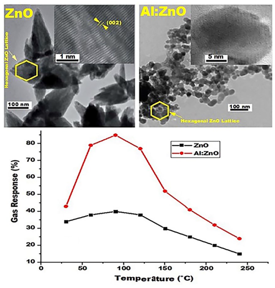
AFM was used to examine the pure and doped films prepared by the atomization method. Figure 2 shows the pure and Al-doped films as three- and two-dimensional (AFM) images. An increase in the weight percentages of aluminum to 0.09 wt% leads to an increase in the surface roughness properties of the film, such as the root main square (RMS) by 57.4% compared to the RMS of the pure zinc oxide film surface. 39 In contrast, the Hall measurements of the pure and doped films revealed the type of charge carriers and the possibility of calculating their concentrations and Hall motilities. At the laboratory temperature, it was found that all the aluminum-doped ZnO films were the n-type, and this is due to the behavior of aluminum atoms as donor impurities in the polycrystalline ZnO films and because the aluminum atoms occupy the substitutional sites for zinc, as is the case in single crystals. Thus, the concentration of charge carriers increases. However, Figure 3 shows the high-resolution transmission electron microscopy (HR-TEM) images and energy-dispersive X-ray (EDX) analysis of Al:ZnO thin films for pure ZnO and that with 0.09 wt% of Al3+ doping. The TEM image with a 5 nm scale bar shows the high orientation toward the c-axis, with a hexagonal structure, especially for the (002) plane. HR-TEM supports the results where the crystalline and optical properties of the ZnO:Al thin films are improved with increasing Al3+ concentration. Also, EDX show the main elements are Zn, O, and Al on the surface of pure and Al:ZnO films at room temperature. 40

(a) HR-TEM of ZnO, (b) HR-TEM of 0.09 wt% Al:ZnO, (c) EDX analysis of pure ZnO, and (d) EDX analysis of 0.09 wt% Al:ZnO at room temperature.
Annealing temperatures and conductivity
Figure 4 shows the conductivity values with doping at laboratory temperature before and after annealing at a temperature of 200 °C for 20 min in argon gas. We noticed that the conductivity for the prepared films increased non-linearly with doping. This non-linear behavior is because at low doping, ions (Al3+ ions into Zn2+) are displaced, and because the valence of Al is higher, the aluminum atoms occupy the place of the zinc atoms, and thus they behave as the donor atoms.

Conductivity values of Al:ZnO films at different Al-doping weight ratios before and after annealing at 200 °C for 20 min.
Ionizing leads to an increase in the charge carriers, which leads to an increase in conductivity, but by increasing the percentage of doping further, the Al3+ ions behave as impurity-scattering centers called scattering natural impurities center. Due to the small size of the aluminum ion compared to the zinc ion, these centers lead to shrinkage of the crystalline lattice, and this works to create levels at the surface of the membrane and at the granular borders, which are linked by loose bonds that snipe the charge carriers generated from the doping, forming charged barriers that stand in their way and disperse them, which leads to a drop in conductivity.
When annealing these films, we noticed that the conductivity increases because the annealing works to increase the size of the crystalline grains, and thus, the granular boundary voltages decrease, which increases the electronic free path and then increases the electronic mobility leading to improvement in conductivity. Figure 4 shows the conductivity values on doping at 25 °C before and after annealing at 200 °C for 20 min.
The annealing process at high temperatures leads to an increase in electrical conductivity as a result of oxygen absorption from the Al:ZnO films. 41
Number of charges and electronic mobility rate
Figure 5(a) shows the number of charge carriers for the prepared and thermoplastic films. We note that the number of charge carriers prepared by the spraying method was large, and this is because the prepared films were of high homogeneity, and this leads to a decrease in the voltage ratio at the granular boundaries. Thus, the charge carriers are not dispersed. The number of charge carriers increases with an increase in the aluminum concentration in the film. This is because increasing the amount of aluminum or alumina not only enhances the amount of charge but also enhances the improvement of the surface charge of active adsorption. 42
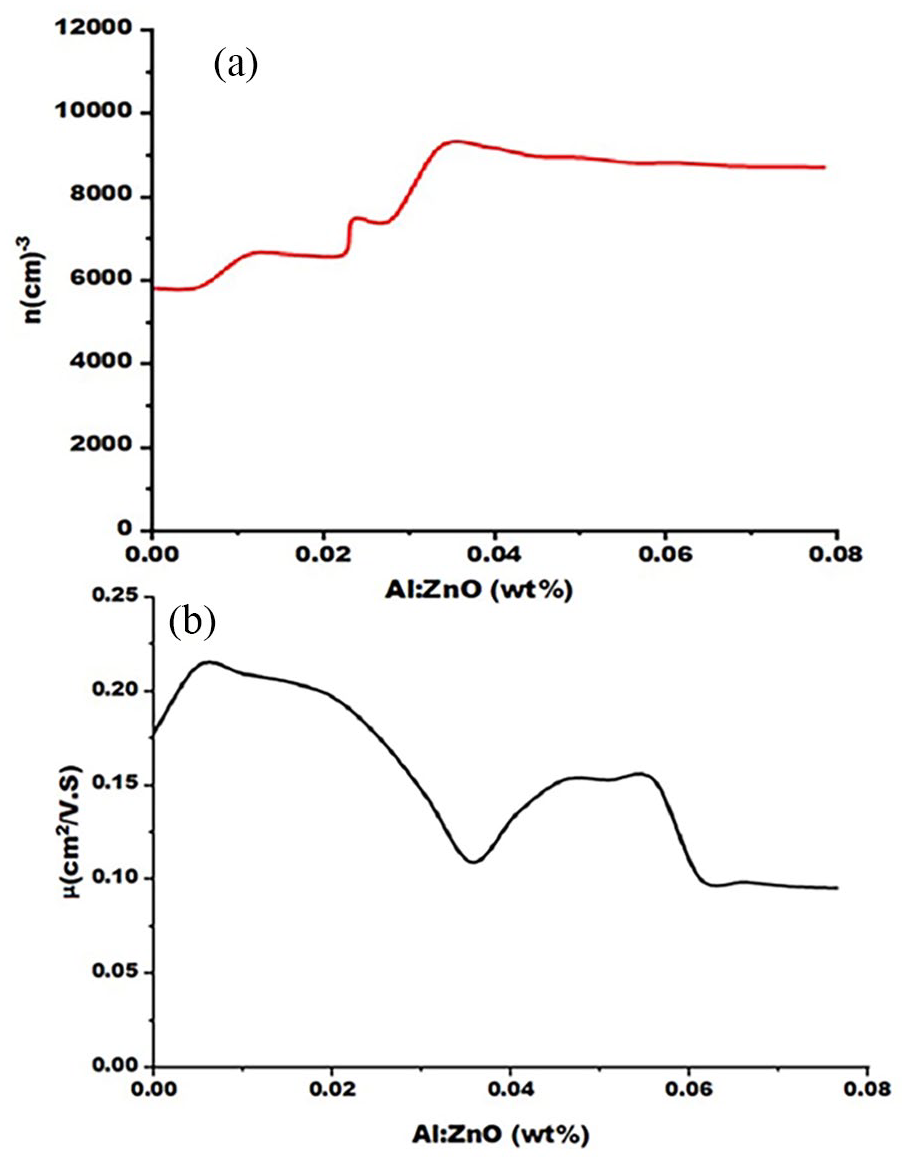
(a) Number of charge carriers at room temperature and (b) the electronic mobility rate of the films prepared before annealing as a function of the Al-doped weight ratios.
In Figure 5(b), we notice that the rate of electronic mobility increases slightly with low doping and decreases with increasing doping until it reaches its lowest value (0.1 cm2 (V.s)−1) at a doping ratio of 0.035%. This is due to the liberation of some charge carriers in a manner that does not affect mobility. In the case of low distortion, as for the increase in doping, it leads to an increase in the number of charge carriers at the granular boundaries and, thus, a linear increase in the charged electrostatic barrier caused by these trapping carriers at the granular boundaries, which disperse the original charge carriers and reduce mobility. As is known, the mobility of charge carriers in semiconductors is inversely proportional to the saturation ratios. Increasing the weight ratio of aluminum in ZnO film leads to an increase in the absorption rate and a decrease in the permeability, which impedes or reduces the movement of free electrons from aluminum to the zinc oxide film. 43
Effect of gas pressure on thin film conductivity
A sample of the thin film prepared by the atomization method was placed in an airtight container with a capacity of 0.227 m3 containing carbon dioxide gas. The film with a doping percentage of 0.03 wt% was annealed for 20 min at 100 °C–200 °C. The container was then emptied of air. After allowing CO gas to enter the container through the pressure gauge valve, we controlled the amount of gas entering, as shown in Table 2, and took readings from the pressure gauge connected to the airtight container.
The pressure values (bar) and the concentrations of CO.

The electrical conductivity of the thin film can be determined due to the reduction of the gas to oxygen, which raises its conductivity, and the gas concentration was calculated from the general gas law 44

where P is the pressure (bar), V is the volume of the gas (m3), n is the number of moles of gas (mol), R is the general constant for gases (8.314 J mol−1.K), and T is the temperature (K).
The gas concentration (C) in (mol m−3) is calculated from the equation 44
Figure 6 shows the relationship between the conductivity and gas pressure, which depends mainly on the gas concentration (Table 3). Model 5 in Table 3, represented by 0.03 wt% of Al-doping, increased the conductivity by 85% at a pressure of 0.4 bar and a concentration of 63 ppm of carbon dioxide gas. We noticed that the increase in conductivity was linear at first and then deviated. After 2 min of exposure to CO gas, it shows linear behavior. The value approaches saturation at a pressure of 0.8 bar and a concentration of 94 ppm with an increase in conductivity by 160%. Based on the above results, these thin films can be used as sensors for carbon monoxide gas. 18 The results show that ratios of 0.03, 0.05, and 0.09 wt% gave suitable sensors for carbon monoxide gases.

Relationship between the conductivity of a 0.03 wt% sample with the respect to pressure of CO gas.
A comparison between the sensor properties of previous studies, including sensing temperature, carbon dioxide concentration, and sensitivity, and the properties of the sensor.

TS: type of sensor; ST: sensing temperature; CC: CO concentration; S: sensitivity, RT: room temperature.
Comparison of the sensors for CO detection
Figure 7 shows the relationship between thin film conductivity and CO concentration for pure ZnO and Al:ZnO films when carefully inserted into the space containing the sample. The samples were kept under a vacuum of 3 × 10⁻³ mbar during the electrical measurements to keep the samples free from any other effects. The conductivity was found to increase linearly with the concentration of CO gas for Al:ZnO and non-linearly for pure ZnO. The sensitivity at 114 ppm of CO increased from 30 for a pure sample to 110 (ῼ cm)−1 per mole for the doped sample. Therefore, the sample sensitivity for CO increased by more than three times at 0.03% Al-doping. Some of these results indicate that ZnO films can be used as gas-sensing elements. 49 This increase in conductivity is because CO gas is characterized as a strong reduction impurity. However, the oxygen chemisorption creates a surface barrier at the grain boundaries, acting as electron traps and consequently leading to a conductivity decrease. 50 In contrast, introducing CO will reduce the chemisorbed oxygen or some internal oxygen, and any oxygen reduction will increase conductivity.

Relationship between the conductivity of pure ZnO and Al:ZnO films and the CO concentration.
Gas response of thin films
The detect ions of harmful concentrations of carbon monoxide vapors using thin films manufactured from pure and Al:ZnO films were based on the thickness of these films, after studying the effect of high temperatures on the electrical properties of these films. The gas response is calculated according to the following formula 38

where Ra is the response of the sensor in the presence of O2 and Rg is the response of sensors in the presence of the analyzed gas. The sensors are greatly affected by high ambient temperatures, which are a critical factor in the investigation of gas sensing, from temperatures as high as 240 °C to as low of 30 °C. Figure 8 shows the response curves at different temperatures from 240 °C to 30 °C for pure ZnO and the Al:ZnO sensors. The response increases with increasing temperature, and this behavior can be explained as follows. The sensor response to a reducing gas, such as CO, depends on a sensitive reaction balance between the adsorption and desorption rates of carbon monoxide and the surface reaction of adsorbed CO with the adsorbent type of oxygen. The increased operating temperature is favorable for the chemical absorption of CO to some extent, and the reaction rate occurring on the ZnO surface results in an enhanced gaseous response. At higher temperatures, the gas response is reduced due to the adsorption of CO, which reduces the amount of carbon dioxide absorbed on the ZnO surface. However, the Al-doped sensors appear to be strongly, preferably being sensitive to carbon monoxide. 51 We note that the undipped ZnO sensor had a response rate to carbon monoxide gas of 40% at 90 °C, while the response rate to carbon monoxide gas by Al:ZnO was 85% at 90 °C.

Response to CO gas of pure ZnO and Al:ZnO thin films at different temperatures.
PPM variation of CO gas with the prepared films
The effect of the carbon monoxide gas concentration on the developed sensor was examined by studying the minimum and maximum response of the sensor when the starting low gas concentration increases from 16 to 100 ppm (Table 2). The responses of the fabricated sensors, which were tested at different CO concentrations and an operating temperature of 200 °C, are reported in Figure 9. Pure ZnO and 0.03 wt% Al:ZnO allows a remarkable enhancement of the sensing characteristics toward CO. Furthermore, the high response of these sensors can also be observed on exposure to low CO concentrations. No saturation of the sensor response was observed at the highest concentration of CO tested (80 ppm). These results agree with the previous study. 51

Response of the ZnO and Al:ZnO thin films as a function of CO concentration at a temperature of 200 °C.
Reusability study
Work was done to repeat the sensing results with the pure zinc oxide and Al:ZnO sensors to investigate their efficiency, as repeating the sensing results is considered a measure of the robustness of the sensor in detecting carbon monoxide gas. Use the ideal temperature and gas concentration for high gas response with the 90 °C and 80 ppm, which were discussed in the previous paragraph, and the process is repeated four times every 2 days to verify the reusability of the sensor. The results of repeated testing of the response showed a slight change from a slight decrease in the activity of the sensor surfaces, which at the same time affected the oxidation properties of the sensor, as shown in Figure 10.

A reusability study of Al:ZnO and pure ZnO sensors at a CO concentration of 80 ppm.
Comparison of the prepared sensor
The sensors in this study were produced using the sputtering method to sense carbon monoxide gas, and the produced sensors were compared with several sensors reported in the scientific literature, whether these were designed to sense carbon monoxide gas or many gases.
This comparison focuses on several parameters, such as the gas concentration used, the temperature that best responds to the gas by the sensor, the production method, and the type of sensor (Table 3).
Conclusion
Thin films are important for studying the photoelectric, electromagnetic, mechanical, and chemical properties of most solid engineering materials, which are difficult to see and sense when the engineering materials are in their natural form. Therefore, thin films of ZnO:Al were prepared by sputtering with multiple concentrations of Al3+ to determine these properties for engineering applications, such as gas sensors. Several tests were used in this study, including XRD, AFM, HR-TEM, and EDX. The results demonstrated that the conductivity, mobility carriers, and carrier concentration increased with increasing Al3+ concentration. Also, Al:ZnO film with a (002) plane and 2θ ≈ 34° has high homogeneity and orientation, besides improving the surface roughness properties of the films. However, the annealing process at high temperatures increases the electrical conductivity due to oxygen absorption from the Al:ZnO films. The Al3+ also enhances the response of the sensor to carbon monoxide gas at 90 °C. In addition, the sensors produced work to detect low concentrations of gas and the saturation state is not observed. The process of repeated reusability showed a slight decrease in the response percentage.
Experimental section
Materials
Zinc oxide particles (CAS 1314-13-2), purity ⩾ 99.0% and 81.39 g mol−1 molar mass, pure aluminum (granulated) with purity ⩾ 99.0%, (CAS 7429-90-5), and molar mass 26.98 g mol−. Hydrochloric acid fuming (37%) and acetone with purity ⩾ 99.8% and (CAS 67-64-1). All materials were obtained from Merck KGaA, Darmstadt, Germany.
Preparation of doped film samples
In this work, pure ZnO films and ZnO:Al-doped films were prepared with different weight ratios of Al using the spraying method. This technique is considered a new method for solid film deposition, in which atoms are expelled from a solid when subjected to bombardment with high-energy particles, and this process is usually used for thin film deposition.
However, 10 wt% of ZnO particles were dissolved in dilute hydrochloric acid to prepare a 0.6 M ZnO solution and 1 wt% of pure aluminum was dissolved in dilute hydrochloric acid to prepare a 6 × 10⁻⁴ M Al solution. The ZnO solution was mixed with the Al solution in a proportion by weight, as shown in Table 4, and acetone was added to the above mixture and re-stirred continuously using a lid prepared to obtain good homogeneity. This mixture was pressed to form disks considered targets in the atomizing system; this process was repeated for each sample. The system consists of a cathode, which is in the form of a disk of a material with good electrical conductivity, such as copper. The target is attached to the cathode, and it must be taken into account that the diameter of the target is greater than the diameter of the cathode to avoid atomization of the cathode material, noting the need to isolate the cathode system from the rest of the parts of the device. An insulated ring is placed around the cathode to prevent dissolution of the cathode and keep it in the correct direction. The cathode material may be surrounded by a copper tube through which cold water passes to cool the cathode when sedimentation is used for a long period. The anode consists of a substrate holder, and the floor is grounded and has a biasing voltage, and it is heated to obtain the appropriate floor temperature, as shown in Figure 11. The spraying process occurs when it affects the target with a continuous voltage in the range of 0.5 kV, and this voltage generates an electric field, the value of which depends on the magnitude of the voltage used. In this case, the neutral and continuously flowing argon gas atoms will ionize inside the vacuum vessel into positive ions, and electrons precipitate the positive ions to the surface of the target. Next, the target is bombarded at a certain energy, and as a result of this bombardment, the atoms are removed from the surface of the target and thus stick to the glass slides in the ground carriers.
The solution weight ratios of pure and doped ZnO film samples.

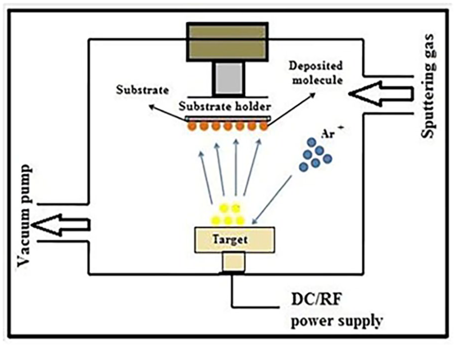
Schematic of sputtering device used.
Characterizations
To obtain the required properties of pure and doped ZnO film samples, the following devices and equipment were used to complete this research. The surface topography of the pure and doped ZnO film samples was measured by AFM (Naio AFM 2022, Nanosurf AG, Switzerland), and the roughness surface properties were measured with Mountains SPIP® Academic 9.3.10249 software. The crystal properties were evaluated by XRD (D8 Bruker, Germany), and data were collected at 0.02° intervals with a count of 0.5 s per step in the 2° range of 5°–80°.
Footnotes
Acknowledgements
The authors thank everyone who helped to complete this work, especially the employees in the Polymer Department’s laboratories, CAK Company, and Tabriz University.
Declaration of conflicting interests
The author(s) declared no potential conflicts of interest with respect to the research, authorship, and/or publication of this article.
Funding
The author(s) received no financial support for the research, authorship, and/or publication of this article.