
Abstract
In this work, tungsten oxide thin films are deposited on silicon substrates using the hot filament chemical vapor deposition system. The influence of substrate temperature on the structural, morphological, and elemental composition of the tungsten oxide thin films is investigated using X-ray diffraction, field-emission scanning electron microscopy, and X-ray photoelectron spectroscopy techniques. Also, the mechanical and tribological properties of these thin films are considered using nanoindentation and scratch tests. Based on X-ray diffraction results, it can be concluded that tungsten oxide thin films are synthesized with a cubic WO3 structure. From field-emission scanning electron microscopy images, it can be seen that tungsten oxide thin films are made of crystal clusters which have grown vertically on the substrate surface. In addition, the results exhibit two asymmetric W4d5/2 and W4d7/2 peaks which can be assigned to W5+ and W4+ species, respectively. The mechanical results show that the hardness and the elastic modulus increase on raising the substrate temperature up to 600 °C. From the tribological performances, the friction coefficient of the tungsten oxide thin film decreases on increasing the substrate temperature.
Keywords

Introduction
Tungsten trioxide (WO3) is a wide band gap metal oxide semiconductor having interesting properties for numerous applications, such as electrochromism, gas sensing, and thermoelectric and catalytic properties, and it has been studied extensively.1–3 Films of WO3 have been deposited by a number of techniques including vacuum evaporation, reactive sputtering, and chemical vapor deposition (CVD).4,5 Moving the substrate through the CVD reactor allows continuous growth and avoids downtime. In previous work, 6 it has been shown that direct deposition of tungsten oxide is possible at atmospheric pressure by pyrolytic decomposition of tungsten hexacarbonyl. This technology yields films with mostly amorphous and highly porous structure, which is desirable as it enhances ion mobility. 7 The film structure is strongly influenced by the deposition temperature (i.e. substrate temperature) and the oxygen content in the gas environment during film growth. A surfactant- and polymer-free, single-step aerosol-assisted chemical vapor deposition (AACVD) method has been used to synthesize tungsten oxide thin films nanoneedles decorated, which provides for direct integration of the nanomaterial with gas-sensing platforms.8,9 A survey of the literature suggests that the coloration efficiency of CVD WO3 films is comparable with that of those prepared by evaporation, electrodeposition, or sputtering. The atomic pressure chemical vapor deposition (APCVD) process for making tungsten oxide films using volatile liquid tungsten pentacarbonyl pentylisonitriles as precursors has been reported. 10 Also using hot filament chemical vapor deposition (HFCVD) method, several structures of tungsten oxide has been reported and the results suggested that by controlling the growth parameters, the properties can change.11–13
On the other hand, coatings of tungsten oxide thin films are known for their high hardness and great wear resistance, tungsten oxide being the best known member of the transition oxides family. Tungsten oxide has an excellent lubrication performance with low tribo-oxidation sensitivity and its tribological properties depend on the temperature; thus, due to its rapid oxidation, when the coating is exposed to high temperatures, its tribological properties are diminished greatly. 14 Adhesion and mechanical properties are issues in defining the stability of thin films and coated samples and their performance in different environments. In the fields of the hardness, scratch resistance, and wear behavior of WO3, a few reports are available which have focused on the mechanical and tribological properties of WO3 films deposited on metal substrates.15–17 These reports describe investigation of the mechanical and/or tribological properties of tungsten oxide films of micrometer-scale thickness using micro-scale measurements. Whereas the physical properties and characteristics of the tungsten oxide films strongly depend on the conditions and methods used for their deposition and preparation,16,17 plenty of techniques have been applied in order to improve the properties and fabrications of tungsten oxide nanostructures, such as spray pyrolysis, pulsed-laser deposition, chemical vapor deposition, sputtering, electrodeposition, sol–gel methods, and thermal evaporation.17–19 The aim of this work is to study the influence of substrate temperature during the deposition process on the structural and mechanical properties of tungsten oxide thin films. For this purpose, in this work, we have described our experimental results on the formation of tungsten oxide thin film, which clearly demonstrates the effect of substrate temperature on its morphology, structure, and elemental composition, using X-ray diffraction (XRD), X-ray photoelectron, and field-emission scanning electron microscopy (FESEM). In addition, the mechanical and tribological properties of these films have been investigated.
Result and discussion
The XRD patterns of tungsten oxide thin films for three substrate temperatures are shown in Figure 1. The results show that all the XRD peaks could be included in a cubic WO3 structure.20,21 As the substrate temperature increases, the number of sharp XRD peaks increases such that the XRD peak positions are identical because of the increasing thermal mobility of the active atoms near the silicon substrate surface. By increasing the substrate temperature to 600 °C, the (122) peak intensity is increased and the diffraction peaks were indexed to (112), (110), (101), (201), and (202).11–13,20,21 However, the intensity of each diffraction peak is different and at a higher substrate temperature (T = 600 °C), all the structures are well crystallized. There are different peak intensities in the XRD pattern related to different substrate temperatures. At higher substrate temperatures, atoms near the substrate surface have enough temperature to form a well-crystallized structure, while at lower substrate temperatures, relatively weak diffraction peaks were observed (Table 1). Peak intensities are normalized to (122) and as the substrate temperature increased from 400 °C to 600 °C, several new strong Bragg peaks appeared and a polycrystalline structure forms (see Table 1). Here, we use Scherrer’s method to calculate the crystalline size, which is widely used to calculate grain size in metal oxide and nanoparticles. Using the full width at half-maximum (FWHM) of WO3 (122) peak from Scherrer’s method, the average crystalline size of the tungsten oxide thin film can be calculated (equation (1)) and the results are presented in Table 1

where k is the shape factor (0.94), λ is the wavelength of Kα Cu radiation (1.5406 Å), and β is the FWHM. It is observed that the crystallite size increases on raising the substrate temperature during the growth process. This means that the preferential orientations of crystal growth are strongly dependent on substrate temperature. These results agree with the results of Miao et al., 22 Yavada et al., 23 and Ikhmayies et al. 24 The maximum crystallite size is found to be 70 nm for T = 600 °C. 12
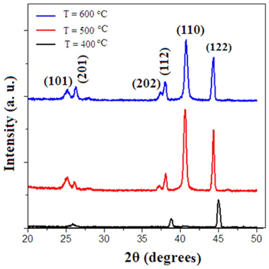
XRD spectra of WO3 thin films at different substrate temperatures: 400 °C, 500 °C, and 600 °C.
Identification of the XRD peaks shown in Figure 1.

FWHM: full width at half-maximum; XRD: X-ray diffraction.
The elemental and chemical characterizations of the WO3 thin film at different substrate temperatures were performed by X-ray photoelectron spectroscopy (XPS; Figures 2 and 3). For all three WO3 thin films, the core level spectra of W4f are observed around binding energies of 31 and 33 eV, which are related to W4f7/2 and W4f5/2, respectively, and are in agreement with previous results.5,11 The height of core level decreased after increasing substrate temperature, which implied increased oxidation states of W in the WO3 film and this film exhibited a larger degree of oxidation state. 11 The peaks located around 35 and 38 eV are W4f7/2 peaks of metallic tungsten for each sample. The ratio of these two peaks is ∼0.8, which is supported by the spin-orbit splitting theory of 4f levels. Moreover, the structure was shifted toward higher energy relative to the metal state. It is thus clear that the main peaks in the typical XPS spectrum are attributed to the W6+ state on the surface indicating that the deposited film is composed of stoichiometric WO3.25,26 Also in Figure 3, the XPS analysis yielded the value for the bond energy of the O1s electrons around the binding energy of 535.5 eV. The O1s spectrum of each sample includes a main contribution at the lowest binding energy with approximate Gaussian distribution originated from the W-O bond. In addition, the O1s peak moves significantly with deposition temperature, which the higher binding energy peak is attributed to the oxygen vacancies in the WO3. 26 By increasing the temperature, the surface oxygen vacancy content decreased. 27 Vasilopoulou et al. reported that WO3 is similar to MoO3 in crystal and energy band structures. Therefore, a certain degree of oxygen vacancies results in the occupation of large density of states lying within the forbidden gap and conduction band with a corresponding shift of the Fermi level toward higher energies. 28

W4f XPS spectra of WO3 thin films at different substrate temperatures: 400 °C, 500 °C, and 600 °C.

O1s XPS spectra of WO3 thin films at different substrate temperatures: 400 °C, 500 °C, and 600 °C.
Figure 4 shows FESEM images of the tungsten oxide thin films grown at different substrate temperatures. It can be seen that the tungsten oxide thin films are made of crystal nanoclusters with sizes of about 40–70 nm, while the largest cluster size is at the highest substrate temperature. The dashed line in Figure 4(a), (c), and (e) indicate a random measurement of particles, but in general, the size of the clusters increases with temperature. Also, it is visible that the boundaries between the clusters appear more clearly with increasing substrate temperature, confirming that increasing the substrate temperature creates more space between the clusters.15–17 However, a higher substrate temperature expands the growth and nucleation rate, so that the increase in substrate temperature may be related to the enhancement of activated radicals and number of atoms near the silicon substrate, which is in agreement with the XRD patterns. Also, it is reported that the critical nuclei size increases on increasing the substrate temperature and the barrier for nucleation is greater with increasing temperature;16,17 this process can be seen in the scanning electron microscopy (SEM) images. The conglomeration of smaller size grains can be activated by greater energy due to the increasing substrate temperature which causes more mobility of atoms and hence resulting in the larger sized structures. The surface morphology of the deposited thin films in Figure 4(a), (c), and (e) shows more heterogeneous distribution of grains with the increase in the substrate temperature that may be due to the more grains growth. In addition, it could also be observed that all of the films are very dense and the interface between the film and substrate gradually became ambiguous, which could be caused by the increase of diffusion of WO3 into the substrate with the temperature increase.

Top view of SEM images of WO3 thin films at different substrate temperatures: (a) 400 °C, (c) 500 °C, and (e) 600 °C. Cross sections of SEM images of WO3 thin films at different substrate temperatures: (b) 400 °C, (d) 500 °C, and (f) 600 °C.
To calculate the thickness, cross-sectional features of the samples were obtained by FESEM. The thickness is estimated to be around 1–3 µm. From cross-sectional FESEM images, columnar grain growth with a spindle-like shape is observed when the substrate temperature is increased.
Figure 5 shows the variations of the coefficients of friction obtained from the scratch tests. Also, Figure 6 shows the variations of the lateral force/normal force of the sample deposited at 600 °C substrate temperature as a function of time, in order to obtain the coefficient of friction. As can be seen in Figure 5, the friction coefficient of the tungsten oxide thin film decreases on increasing the substrate temperature. According to previous research results, the friction coefficient of the thin films in the steady-state phase was dependent on their microstructures. 29 As a matter of fact, the sample deposited at 400 °C with a denser microstructure results in a lower friction coefficient. The lubricant WO3 thin films are too thin to separate asperities of the contacting surfaces. These rough films however can be highly protective. Comparison of the results of the wear test revealed that the performance of the coatings at different substrate temperatures is very different. This can be attributed to the wearing mechanism of the coatings. The tribochemical reactions occur at the surface of the abrasion where the reaction products are deposited inside the cavities. This action causes the formation of a mixture of reaction products on the surface. From comparing the friction coefficients of the WO3 thin film coatings, it is clear that the coating will reduce the friction coefficient at higher substrate temperature. It has been reported that the dominant mechanism in the wear of WO3 is sticky type and WO3 can form Magneli phases which consist of regularly spaced shear planes with long range order. The variation of scratch volume of all the samples as a function of substrate temperature is shown in Figure 7. As can be seen, the scratch volume decreases on increasing the substrate temperature. This scratch volume behavior is similar to the variation of the friction coefficient and depends on the film microstructure. In fact, denser microstructures have lower scratch volumes.30,31
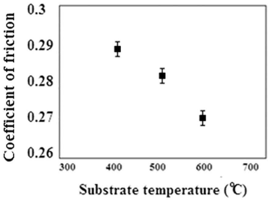
Variation of the friction coefficient of samples as a function of substrate temperature.
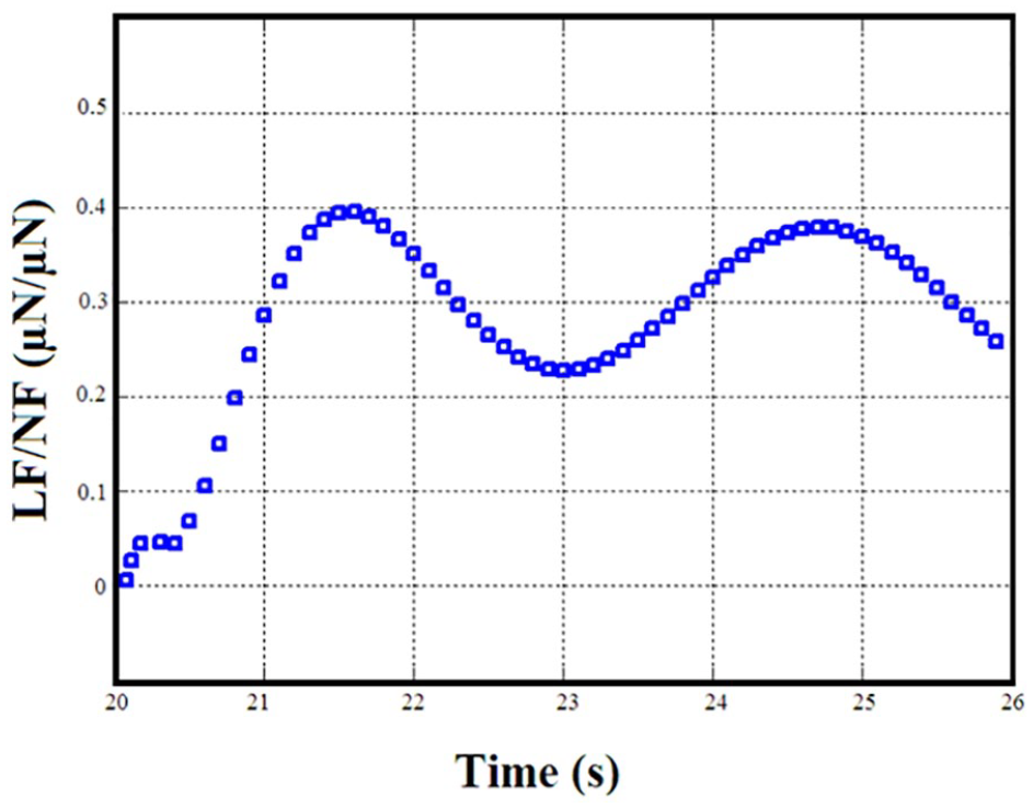
Variation of the lateral force/normal force as a function of time of the selected sample (with a substrate temperature of 600 °C).

Variation of the scratch volume of the samples as a function of substrate temperature.
Figure 8 illustrates the variation of hardness and the elastic modulus of all samples as a function of substrate temperature. The results show that both these quantities increase on increasing the substrate temperature up to 600 °C. The thin film mechanical properties can be influenced by different parameters such as film density, grain size, crystallographic orientations, lattice parameters, and stoichiometry. 32 In this particular case, deeper grain boundaries such as Figer act as an impediment to the dislocation motion because dislocation must change the direction of motion due to the different orientations of grains and also the discontinuity of slip planes from one grain to another.33,34

Variation of hardness and elastic modulus of samples as a function of substrate temperature.
Conclusion
The effect of substrate temperature on the structural, morphological, and mechanical properties of WO3 thin film has been observed. WO3 thin films were grown directly on a silicon substrate using the HFCVD method. XRD, XPS, and FESEM were employed for the study of the nanostructure and surface morphology. The mechanical and tribological properties of these layers were also evaluated using nanoindentation and scratch tests. The XRD patterns and XPS results confirm the cubic phase of the WO3 structure. The results also showed that the scratch volume and friction of coefficient decreased on increasing the substrate temperature, while the crystallite size, hardness, and elastic modulus also increase.
Experimental details
Various methods have been used for the characterization of tungsten oxide thin films. Using XRD, crystalline structures were analyzed. For this purpose, the diffraction patterns were recorded on an STOE-XRD diffractometer with Kα Cu radiation (λ = 1.54060 Å), with a scanning rate of 0.2 s at 2θ = 20°–50° and a step size of 0.02°. By FESEM (Leo 440i), the surface morphology was studied. Using XPS (Thermo Scientific, K-Alpha), the elemental composition was measured. Finally, for mechanical testing, a Hysitron TriboScope nanomechanical instrument with a two-dimensional (2D) transducer (Hysitron Inc., Eden Prairie, MN, USA) and a Berkovich diamond indenter were used. Tungsten oxide thin films were deposited on a silicon substrate using a HFCVD system composed of a stainless steel chamber, a gas mixer, gas cylinders, and vacuum pumps. A tungsten filament was used as the vapor and heating source. The temperature of the hot tungsten filament was kept at 1700 °C, while the distance between the filament and the silicon substrate was 1 cm. To provide vacuum conditions with a rotary vacuum pump, the chamber was first pumped to 1 × 10⁻⁵ Torr in the presence of high-purity argon gas. Subsequently, the substrate was heated to the desired temperature and a mixture of Ar/O2 = 85/15 gas was introduced into the chamber. The experiment was repeated at three different substrate temperatures: 400 °C, 500 °C, and 600 °C. The chamber was cooled to room temperature under an Ar flow and the tungsten oxide thin films were produced on the silicon substrate. Due to the limitations of the temperature range of the heater, the maximum substrate temperature was considered to be 600 °C.
Footnotes
Declaration of conflicting interests
The author(s) declared no potential conflicts of interest with respect to the research, authorship, and/or publication of this article.
Funding
The author(s) disclosed receipt of the following financial support for the research, authorship, and/or publication of this article: The authors are grateful to the National Natural Science Foundation of China (Grant No. 51875342) for financial support of the work reported in this article.