
Abstract
Dielectric actuators are utilized to convert electrical power into mechanical strain with considerable potential in microrobotic applications. However, critical challenges that need to be addressed include high-voltage interface with high conversion ratio, light weight, small size, and high power density. This study proposes a high piezoelectric transformer-based high conversion ratio interface that is integrated with a direct current/direct current high conversion ratio boost stage and a direct current/alternating current high-voltage driving stage. A piezoelectric transformer-based class-E zero voltage switching direct current/direct current interface is controlled by a hybrid pulse frequency modulation and pulse width modulation control strategies to obtain the desired high step-up ratio in the direct current/direct current stage. A half-bridge converter with special digital control algorithm in the direct current/alternating current stage is designed to convert high direct current voltage into arbitrary unipolar signal driving dielectric actuators. A prototype 23.3 g and 4 W interface has been fabricated for experimental validation to verify its ability to drive a 1 kV input dielectric actuator at 5 Hz in microrobotic applications.
Keywords
Introduction
Many types of microrobots are categorized as bionic robots which are designed to achieve compactness, high controllability, and remote monitoring. 1–2 The actuators as critical exciting sources are capable of achieving desirable performance in microrobotic applications. 3–4 The applications of microrobotics, including micro pipe robots, micro air vehicles, and micro underwater robots, among others, have been utilized in many fields. They have advantages that human beings cannot match, thereby enabling these machines to play a huge role in environmental monitoring, 5 geological exploration, 6 personnel rescue, 7 and agricultural production. 8 One of the major challenges in developing a microrobot is achieving motion using limited power supply. In addition, this study presents two major challenges for power electronic design: generating high-voltage drive signals in system typically powered by low-voltage energy sources and recovering unused energy from the actuators.
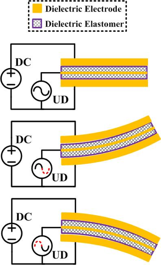
Several biomimetic robots, including legged robots, inchworm-type robots, and flapping wing devices, have been built by using dielectric elastomers. 9 Dielectric actuators (DEAs) have higher energy conversion ratio, mechanical strain, and power density compared with other artificial actuators, such as electromagnetic, 10 shape memory alloy, 11 electrostatic, 12 and piezoelectric actuators. 13 DEAs used in this study are multilayer beams of three conductive and two dielectric elastomer layers. Stress is generated by applying electrical potential between two of the neighboring conductive electrodes. This process leads to an asymmetric stress in the beam, thereby causing bending. Bidirectional actuation is possible by changing the electrodes that can be potentially applied across.
In general, DEAs are driven by conventional power sources, such as chemical battery, supercapacitor, 14 fuel cell, 15 and solar cell, 16 the output voltage amplitude of which is several volts. However, the driving voltage applied on the two compliant electrodes of DEA is required to be as high as 1 kV. 17–18 Thus, an interface with high conversion ratio and sufficient output power in watts to drive DEA are required. Finally, the mechanical efficiency of DEA decreases as the frequency increases; thus, the driving frequency needs to be in hertz.
The conventional boost converters including hybrid voltage multiplier and the tapped-inductor (TPI) boost converter do not apply to this case because of their own limitations, such as low power density and low conversion efficiency. 8 Considering a hybrid circuit consisting of a conventional boost converter cascaded with a switched-capacitor charge pump circuit, the power density is too low due to the large size of the charge pump capacitors. 8 With respect to tapped-inductor boost converter, switching losses seriously affect the conversion efficiency of the driving circuit. 8 Piezoelectric transformers (PTs) used in this work have high conversion ratio and high power density. Furthermore, miniaturization and integration are easily achieved by using PTs with a small number of additional components, which is suitable for driving DEA.
This study aims to describe high-voltage interface to overcome several challenges, such as high conversion ratio, light weight, small size, and high power density in microrobotic application. The section “DEA principle of operations” describes the DEA principle of operations. The section “Proposed interface design and control” of this article describes the class-E DC/DC converter works in zero voltage switching (ZVS) mode, which is integrated with a half-bridge converter, basic operation theory, special control algorithm, and idealized switching waveform for the illustrated interface. The section “Simulation verification” presents the operational simulation using reasonable components as well as provides the design guideline of fabrication. The section “Fabrication specifications and experimental results” illustrates the physical implementation of a driving interface using commercially discrete components. Finally, the last section “Conclusion” presents the conclusion and future research.
DEA principle of operations
A general DEA is a “sandwich” called “bimorph,” which commonly includes compliant electrodes coating both sides of the top and bottom surfaces as well as a dielectric elastomer film at the middle. The method of driving the bimorph is called alternating drive, which requires 2n drive stages per n bimorphs. 1 An optimized driving method enables the sharing of the high-voltage bias between multiple actuators, thereby requiring n drive stages and one bias per n bimorph (see Figure 1).
Schematic of the optimized driving method.
A DC high-drive voltage is applied on two compliant electrodes as bias excitation, and a unipolar driving (UD) voltage is connected to the middle dielectric elastomer film. The described driving architecture behaves with the reduction of the interface size and mass by saving the electronic components because the parallel DEAs are permitted to share one DC high-drive voltage. A DC high-drive voltage and n UD voltage are required in using a simultaneous drive scheme if the n parallel DEAs are driven.
PT is a critical element of the proposed topology. The PT function is implemented by the characteristics of the piezoelectric ceramic materials, including the piezoelectric and inverse piezoelectric effects. PT uses acoustic coupling unlike a conventional transformer that uses magnetic coupling between input and output. An input voltage is applied across a short length of a bar of piezoceramic material, such as Piezoelectric Ceramic Transducer (PZT), thereby creating an alternating stress in the bar by the inverse piezoelectric effect and causing the entire bar to vibrate. The vibration frequency, which is typically within the 10 kHz to 1 MHz range, is selected to be the resonant frequency of the block. Thereafter, a high output voltage is generated across another section of the bar by the piezoelectric effect.
Proposed interface design and control
This study proposes a boost-type direct current (DC)/alternating current (AC) interface that meets the requirement of high conversion ratio of DEAs. A class-E DC/DC converter operating ZVS integrated with a half-bridge converter is employed (see Figure 2).

High conversion ratio converter for driving DAEs. DEA: dielectric actuator.
A multiple-layer PT with single switch in the DC/DC stage is selected to obtain a higher conversion ratio requirement compared with the converters described in the studies by Luo and Ye, Vazsquez et al., and Liao et al. 19 –21 In addition, the DC/AC stage has the ability to efficiently generate the required exciting signal to drive DEAs.
DC/DC stage
This study proposes a DC/DC converter (Figure 3), which is a class-E resonant topology that is suitable for use with a multiple-layer PT. The topology is suitable for step-up application with low component count in microrobotic applications. The PT model is ideally suited for a class-E converter because its equivalent circuit represents the topology-associated class-E converter load. PT provides an appropriate resonant structure in terms of component count in one package.

Topology of the DC/DC stage with the PT equivalent circuit. PT: piezoelectric transformer. DC: direct current.
The typical topology of class-E ZVS converter with PT equivalent circuit comprises a power metal–oxide–semiconductor field-effect transistor (MOSFET) Qi that operates as a switch, an LrCrRr series resonant circuit, a shunt capacitor C 1, a negligible stray capacitor C 2, a choke inductor Li , a freewheel diode Dd , and a capacitor Co . Resistor R is assumed as an AC load and the choke inductor Li is selected to reasonably guarantee that the magnetic flux saturation cannot occur during operation. Two primary operating modes are shown in Figure 4.

Two primary operating modes.
During the switch Qi conduction period (t0 < t < t1 ), 0 ≤ ωt ≤ 2πD, the inductor Li is charged by the input battery source, the current Ii is increased linearly, and the voltage VC 1 across C 1 is zero. The resonant circuit comprises LrCrRr because the capacitor C 1 is shortened by the switch Qi .
The resonant frequency is given by the following equation

The current through the series resonant circuit begins as follows

Consequently, the current through the power MOSFET Qi is given by the following equation

The voltage Vp across the primary side of the transformer is sinusoidal in a negative half-cycle and voltage Vs applied on the secondary side is n times of Vp , which is magnified by PT, where n is the step-up ratio of PT.
The inductor Li transfers the stored energy to PT when the switch Qi is off. The resonant circuit comprises LrCrC 1 Rr that is connected in a series. Hence, the current through the inductor Li is sinusoidal until the conduction of the switch Qi . The resonant frequency is given by the following equation

The current through the capacitor is given by the following equation

The voltage across the capacitor C 1 during this interval is as follows
To achieve ZVS, the voltage across the switch Qi and shunt capacitor C 1 must be zero when the switch Qi is conducted. Thus, the ZVS condition is expressed as follows

Using equation (6) and applying an amp–sec balance to capacitor C 1, the following equations are obtained

Substituting equation (9) into equation (6)

Using equation (10) and applying a volt–sec balance across the choke inductor Li , an expression for input battery voltage V bat can be obtained using the following equation
Rearranging equation (11)

From equations (10) and (12), a relationship between the voltage V bat and VC 1 can be obtained

The current through the series resonant circuit is considered sinusoidal. Therefore, using equation (10) and the Fourier formula, the primary side of the transformer is provided as follows

The AC output voltage Vs , which is amplified by PT, is n times the voltage Vp in half-positive cycle. In each mode, the voltage Vs is rectified by diode Dd and smoothed by capacitor Co as a high DC voltage. Hence, the conversion ratio G of the proposed DC/DC stage can be written as follows
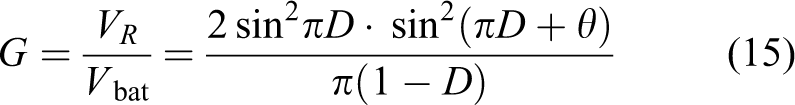
The conversion ratio is higher than the boost converter and TPI boost converter. 20 The conversion ratio versus duty cycle of the three converters is shown in Figure 5 for turns ratio N = 7 and θ = 0.

Conversion ratio versus duty cycle of the three converters (PT specifications are shown in Table 1). PT: piezoelectric transformer.
The shape of the conversion ratio versus duty cycle curve of the PT boost converter is a parabola (see Figure 5). The conversion ratio reaches its peak when the duty cycle is between 50% and 60%, thereby exhibiting a higher conversion ratio than the other two typical boost converters in the low duty cycle.
The step-up conversion ratio G and conversion efficiency of PT are strongly dependent on operating frequency. 22 The required output voltage cannot be regulated and only uses pulse frequency modulation (PFM) because of the resonant frequency character of PT.
In addition, converting an extensive range of input voltage to the desired high output voltage by merely utilizing pulse width modulation (PWM) is impossible. Thus, the single PWM or PFM is not the most suitable control scheme for extensive ranges. Consequently, a new control architecture and the hybrid combination of PFM and PWM can overcome the aforementioned limitations. The required output voltage is obtained via the PWM control with a fixed working frequency combined with the PFM control with constant duty cycle. The operating frequency characteristics of the step-up conversion ratio are illustrated in Figure 6.
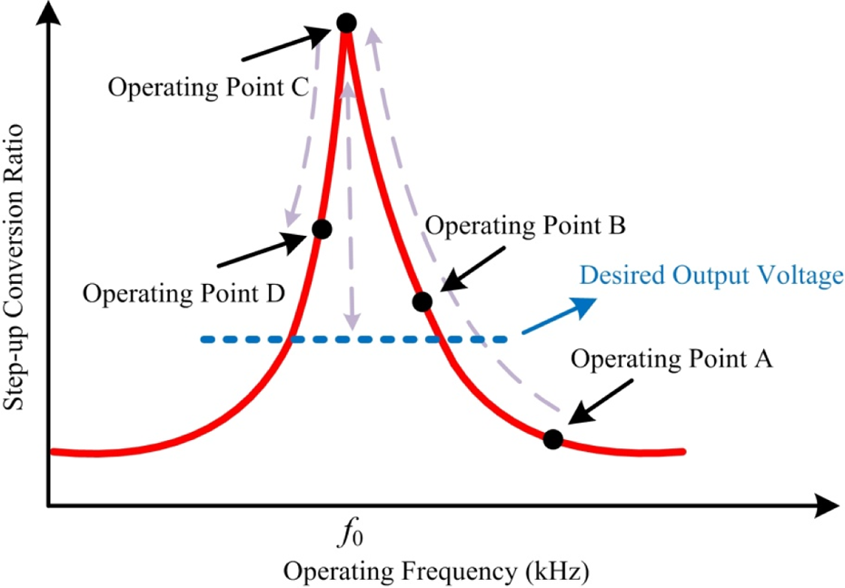
PT with resistive load operating points. PT: piezoelectric transformer.
Maximum conversion efficiency is achieved at a frequency that is the same as the inherent resonant frequency of PT. The operating process starts with a high operating frequency (see operating point A) to avoid the choke inductor Li saturation, which is a relatively low driving voltage applied to resistive load. When the operating frequency is decreased, the step-up conversion ratio increases (see operating point B). As the operating frequency continues to decrease, the maximum conversion efficiency is reached at operating point C and at a certain point between operating points B and D. Varying the duty cycle at operating point C controls the driving output voltage.
A time diagram of the aforementioned hybrid control architecture is shown in Figure 7.
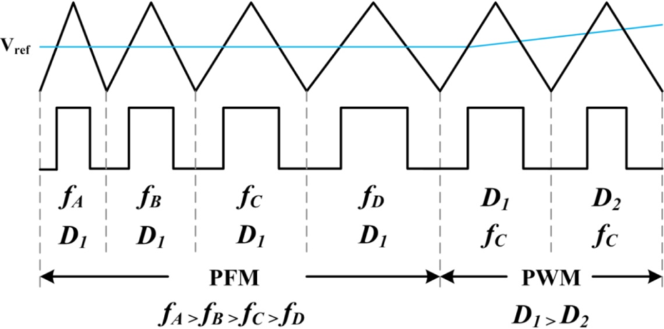
Time diagram of the hybrid PWM and PFM control. PWM: pulse width modulation; PFM: pulse frequency modulation.
Initially, the time of rise/fall edge of the reference signal is changed with a constant duty cycle D1 for the controller. This operation is characterized by the PFM control. When the maximum efficiency point is obtained, the operation mode shifts to PWM by varying the duty ratio. Finally, the desired output voltage is controlled using the PWM control that works at optimized frequency.
DC/AC stage
The DC/AC stage should be able to convert high DC voltage into arbitrary unipolar signal driving DEAs (see Figure 2). Figure 8 shows the four operation modes of the DC/AC stage. The topology operates in mode (a) when switch QH is open and QL is closed. The inductor current begins to increase and the bottom DEA is charged. Thereafter, QH and QL are turned off; the energy stored in the inductor La is decreased via diode Dql (see mode (b)). In mode (c), the switch QL is turned on and QH is turned off. The current passing through the inductor La begins to rise in opposition, and the energy stored in the bottom DEA is transferred to the upper DEA. The energy stored in the inductor La is decreased via diode Dqh when QH and QL are both turned off, and the circuit operates in mode (d).

Four operation modes of the DC/AC stage. DC: direct current; AC: alternating current.
DEAs are often driven by low-frequency sinusoidal voltage at <10 Hz. A method uses an LC resonant network to produce the required driving signal. 23 The sinusoidal pulse width modulation (SPWM) technology requires an inductor and two large additional capacitors. Accordingly, a control architecture is proposed using voltage divider, comparator, lookup table of the desired waveform, and pulse generator for two switches. A real-time pulse signal is generated by comparing the output voltage Va with the lookup table of the desired waveform. Consequently, an arbitrary drive single is produced via a series of control pulse. Figure 9 depicts the waveform of each node during the entire operating cycle.

Waveforms of each node during the entire operating cycle.
Simulation verification
The topology is simulated in MATLAB to make the proposed converter feasible. Table 1 shows the specifications of the utilized components. Meanwhile, components Rr , Cr , Lr , C 1, C 2, and N are the same with the selected PT.
Specifications of the utilized components.

PT: piezoelectric transformer.
For the DC/DC conversion stage, Figure 10 shows the simulated waveforms of the drive signal for the MOSFET Qi , battery source voltage V bat, current Ii through the choke inductor Li , voltage VC 1 across the shunt capacitor C 1, and voltage Vp , Vs , and Vo .
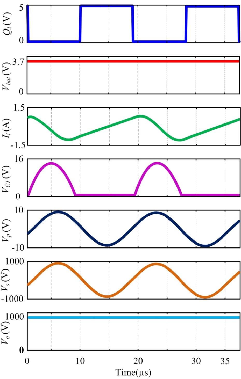
Waveforms of each node in the proposed DC/DC stage. DC: direct current.
The switching frequency of the MOSFET Qi is 55.5 kHz, which is higher than the resonant frequency of PT. A DC voltage of 3.7 V is considered a low-battery source voltage. The current Ii is linearly charged by the battery source when the MOSFET Qi is conducted. Voltage VC 1 is zero in this time interval. When MOSFET Qi is turned off, PT is charged by the inductor Li , and the resonant circuit comprises LrCrC 1 Rr connected in a series. Thus, the current through the inductor Li is sinusoidal until the conduction of switch Qi . Meanwhile, the voltage VC 1 is sinusoidal in positive half-cycle and must return to zero before the switch Qi conduction, thereby guaranteeing that the DC/DC stage operates in the ZVS mode. The sinusoidal voltage Vs (Vpp = 2000 V) applied on the secondary side is n times of Vp (Vpp = 20 V), which is magnified by PT, where n is the step-up ratio of the DC/DC stage. Finally, the voltage Vo is regulated by a rectifying and smoothing circuit at 1 kV DC voltage.
The voltage of VH and VL with respect to the DC/AC stage should meet the stringent requirement of driving signal for DEA. The simulation result is shown in Figure 11.

Simulation results in the DC/AC stage. DC: direct current; AC: alternating current.
The voltage VH and VL are 1 kV sinusoidal signal with 500 V high DC voltage bias (see Figure 11). The two signals are resonant at 5 Hz with 180° phase delay. In addition, the DC/AC stage is capable of generating various types of signals, including the triangle, square, and sinusoidal signals (as illustrated in the section “Fabrication specifications and experimental results”).
Fabrication specifications and experimental results
Fabrication specifications
The circuit described in Figure 2 is soldered on a breadboard using discrete components. Table 2 provides the specifications.
Specifications of the discrete components.

PT: piezoelectric transformer. MOSFET: metal–oxide–semiconductor field-effect transistor.
The proposed discrete components include PT, inductor, power MOSFET, rectifier diode, and capacitor. A commercial through-hole multilayer PT with coupling efficiency above 90% is brought from STEMiNc Corp. to supply sufficient conversion ratio in the DC/DC stage. The two inductors with low-cost, highly efficient shielded inductors (i.e. 10 µH and 15 µH) come from Coilcraft Co., thereby guaranteeing the proposed interface’s normal work. The N-channel IRFBG30 with TO-220 package is selected from Vishay Co. to meet the requirement of high withstand voltage. A low-drop voltage rectifier diode 1N4007 with DO-41 package is employed, which can be salvaged from commercial corporation diodes. A 0.1 µF ceramic capacitor with a through-hole package has the ability to smoothen the output voltage of PT. The PT-based power electronics interface is depicted in Figure 12.
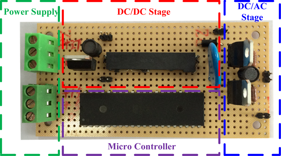
Image of the PT-based interface. PT: piezoelectric transformer.
Table 3 outlines the performances of the proposed interface.
Characteristics of the PT-based power electronics interface.

PT: piezoelectric transformer.
The maximum power density is reached at 0.17 kW/kg when the output power is 4 W. The peak conversion efficiency is 49.5% because the components account for a significant percentage of mass in robotic insects. 2 Thus, discrete components with chip package are considered to substitute that with a through-hole package in further research. Furthermore, the flexible printed circuit board (PCB) technology is introduced for high integration.
Experimental results
Circuit experimental analyses
A low-voltage source lithium-ion battery is utilized to generate high drive voltage in the aforementioned topology. The input voltage V bat of the TP-based boost interface is 3.7 V, and the output voltage Vo is regulated at 1 kV. A 0.25 MΩ pseudo load is utilized, which is consistent with the characteristic of DEA, to demonstrate that the circuit has 4 W output capacity. This interface is capable of generating three waveforms (i.e. square, triangle, and sinusoidal waveforms; see Figure 13).

Output voltages of each node (i.e. V bat, VL , VH , and Vo ) in (a) square driving, (b) triangle driving, and (c) sinusoidal driving modes. Note that the oscilloscope probe is used 50 times to measure 1 kV voltage.
The waveforms, particularly the sine and triangle waveforms do not look excellent (see Figure 13). The phenomena exhibited in this study are caused by the limited quantity of dots in the lookup table. More dots in the lookup table mean better quality of the output waveform. The speed of Analog-to-Digital Converter (ADC) is required at the same time. Thus, the selection of the number of dots is the result of our overall consideration according to the existing conditions.
The gain of the experimental result (shown in Figure 13) is smaller than that of the theoretical value calculated using equation (15). The various loss mechanisms in the circuit (e.g. conduction, switching, and magnetic losses) are able to account for this phenomenon. Moreover, the fluctuation of the clock frequency of the microcontroller leads to the fluctuations of the switching frequency. Therefore, the duty cycle ranges from f ± Δf, where f is the desired switching frequency and Δf is the frequency fluctuation. Consequently, the conversion ratio of the proposed interface fluctuates approximately between 101.6 and 101.7 with a margin of error of 0.05%. Similar results can be obtained for the other two converters. That is, the fluctuation range of the conversion ratio of the boost circuit and TPI boost circuit are from 1.97 to 1.98 and from 8.96 to 8.98, respectively. Their error rates are 0.07% and 0.12%, respectively.
The proposed converter’s conversion efficiency can be calculated as follows

where P load is the average power of the DEA load and P in is the average input power of the described converter.
Figure 14 demonstrates the efficiency of the proposed interface in terms of various loads and driving frequency.
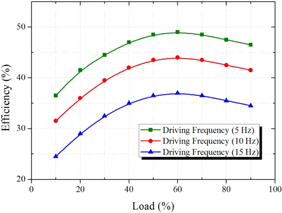
Efficiency versus load for the three different driving frequencies.
The loads continuously increase from 10% to 100% with 10% intervals. The three driving frequencies are 5 Hz, 10 Hz, and 15 Hz. The peak efficiency (49.5%) can be obtained at 60% load and 5 Hz driving frequency (see Figure 14).
Many microrobotic applications are battery-operated systems; thus, the current consumption should be considered. The peak efficiency (49.5%) in the proposed test condition can be obtained at 60% load and 5 Hz driving frequency. The current consumption is calculated as 2.448 mA. Karpelson et al. 1 proposed the topology of a TPI boost converter integrated with a switching amplifier drive stage. The current consumption is 3.532 mA, which is obtained at 200 V output voltage and 100 Hz output frequency. Thus, the current consumption of the topology in this study is smaller than the aforementioned circuit.
DEA driving experiment
The figure 15 is the image of the entire system comprising a battery box, the proposed interface, and a manual probe station that is used in conjunction with the B1505A I/V Agilent Power Device Analyzer.
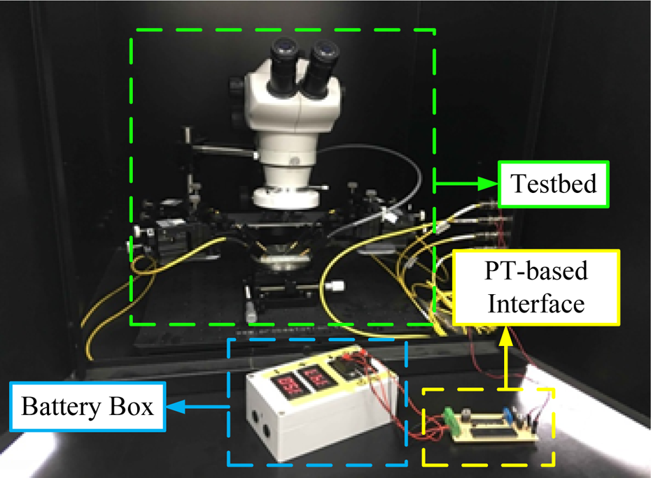
Image of entire system.
The DEA actuator utilized as a prototype to test the performance of PT-based high conversion ratio interface is shown in Figure 16.
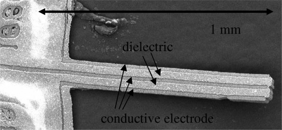
A micro-fabricated bimorph DEA actuator. DEA: dielectric actuator.
The dimensions (i.e. length, width, and thickness) of the DEA actuator are 1000 μm, 100 μm, and 40 μm, respectively. Four images can be obtained when the DEA actuator is driven at four different voltages (i.e. 0 V, 600 V, 800 V, and 1000 V). The final image after being cropped and overlaid is shown in Figure 17.
Deformation images of the DEA actuator, which is driven at four different voltages: (a) 0 V, (b) 600 V, (c) 800 V, and (d) 1000 V. DEA: dielectric actuator.
The red arrow depicts the deformation with the increasing driving voltage. The DEA actuator demonstrates the actuation displacements that approach 350 μm when the driving voltage is 1000 V. The experimental results show that the mechanical deformation is proportional to the square of the driving voltage.
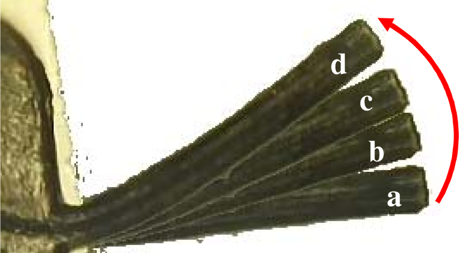
An image of the bidirectional actuation is obtained by providing a driving voltage on the DEA actuator. A similar image can be obtained using the aforementioned method of image processing (see Figure 18). Statuses a, b, and c demonstrate the DEA actuator up, at equilibrium, and down, respectively.

An image of the DEA deformation: (a) up, (b) at equilibrium, and (c) down. DEA: dielectric actuator.
Conclusion
This study has discussed the PT-based high conversion ratio boost interface for driving the bimorph DEA at a system level applied in a microrobotic application. The class-E ZVS high step-up DC/DC stage and DC/AC high-voltage driving stage have been presented in detail. A hybrid of the PFM and PWM control strategies is used in the DC/DC stage instead of a single PWM and PFM control architecture to obtain high step-up conversion ratio and conversion efficiency. Compared with the conventional SPWM, a driving approach has been introduced to convert high DC voltage into arbitrary unipolar signal driving DEAs. A 23.3 g prototype of the proposed interface is developed based on the proposed operating theory and tested with a DEA actuator to demonstrate its driving ability. The peak efficiency (49.5%) can be reached at 60% load and 5 Hz driving frequency, which is higher than the maximum conversion efficiency of 42.4% obtained in Karpelson et al. 1 Moreover, PT used in the current study exhibits high conversion efficiency, no electromagnetic radiation, and small size and is safe and reliable.
Future research can focus on the continued optimization and miniaturization of power electronic circuits. Our succeeding study can improve the efficiency of the system by using ZVS technology, 24 zero current switching technology, and the suppression of switching losses. Moreover, the energy management strategy for the aforementioned topology and the custom-designed bare-die package components are soldered on a flexible PCB to further improve conversion efficiency as well as reduce size and weight to meet the microrobotic requirement.
Footnotes
Declaration of conflicting interests
The author(s) declared no potential conflicts of interest with respect to the research, authorship, and/or publication of this article.
Funding
The author(s) disclosed receipt of the following financial support for the research, authorship, and/or publication of this article: This work is supported by the National Natural Science Foundation of China (grant no. 61403160), China Postdoctoral Science Foundation (grant no. 2014M551194), Science and Technology Office, Jilin Province of China (grant nos 20140520118JH and 20150414052GH).