
Abstract
Back Grinding of Wafer with Outer Rim (BGWOR) is a novel method for carrier-less thinning of silicon wafers. Silicon wafers are widely used in integrated circuits (ICs). The topography of the wafer will not only directly affect the efficiency of subsequent processing of semiconductor devices, but correspondingly affect the performance and life of these devices. However, there are few studies on the shape of the ground wafer in BGWOR. In this paper, the mathematical model of the wafer topography in BGWOR was developed. With this model, the radial thickness and total thickness variation (TTV) of a wafer under different parameters, including inclination angles and radii of grinding wheel for dressing chuck, were simulated by MATLAB. Inclination angles and radii of grinding wheels for the dressing chuck had a great influence on the radial thickness and TTV of a wafer in the BGWOR. Lastly, the pilot experiments were conducted to validate the theoretical model of grinding topography and TTV of the wafer in BGWOR. To enhance the flatness of the ground wafer, it is essential to control the shape of the dressing chuck. The research results are helpful to the optimization of the dressing process of the chuck in the BGWOR.
Introduction
The 3D package is the key packaging technique for integrated circuit chips in the post-Moore’s law era. This technique can increase the number of layers on each chip, which not only reduces the volume of the chip but also abbreviates the path of current. The topography of the wafer will directly affect the number of layers on the chip, and even cause difficulties for subsequent processing. BGWOR shown in Figure 1 is a new method for carrier-less thinning of silicon wafers. BGWOR only grinds the inner circumference and leaves a rim (approximately 3 mm) on the outermost circumference of the ground wafers. Compared with the conventional back grinding (BG) as shown in Figure 2, BGWOR has the advantage of limiting the risk of debris and warpage of ultra-thin wafer.

Illustration of back grinding of wafer with outer rim.

Illustration of conventional back grinding.
Wafer topography is the thickness distribution of a wafer, which is a significant aspect of wafer quality. In pursuance of obtaining better flatness of ground wafer, a prodigious deal of research has been done on the grinding shape and TTV of a wafer in BG.
Oh and Lee 1 experimentally studied the relationship between different reference plane-site, front least square focal plane range (SFQR) and site back ideal focal plane range (SBIR), and TTV of a wafer. They concluded that the TTV was associated with SBIR, but not with SFQR. Chidambaram et al.2,3 and Gao et al. 4 established the mathematical model of the dressing shape of the chuck. The model could attain the shape contour of the chuck according to the set parameters. The simulation outcomes of the model were compared with the experimental outcomes to verify the correctness of the model. Sun et al.5–8 developed the model of grinding marks of a single grain and the mathematical model of the grinding shape of the wafer. Then the adjustment of the wafer surface shape, the impact of the shape of chuck on the grinding marks, and generation mechanisms of central bumps on ground wafers were studied. Chen and Hsu 9 established the mathematical model of the surface profile of chuck, the surface profile of ground wafer, and TTV in BG. They also studied the effect of the angles of the grinding wheel on the shape of chuck and wafer. Afterward, they verified the acquired rule through experiments. Zhou et al. 10 considered the influence of the machine stiffness and the density of grinding marks on the wafer shape, and established the mathematical model of wafer shape. According to the machine stiffness and process parameters, the model could be used to compute the optimal spindle inclination angle of the grinding wheel. Huo et al.11,12 obtained wafers with high surface flatness and low surface damage by using nano-grinding, analyzed the causes and influencing factors of grinding marks in ultra-precision grinding of wafers, and then put forward some measures to suppress the grinding marks.
The above research on the shape and TTV of a wafer is based on the conventional BG. These studies are instrumental to the model development for the BGWOR process, but cannot be applied directly. As far as the authors know, among the published papers, only one paper 13 of our research group studied the BGWOR process. That paper studied the evolution of grinding marks in BGWOR. Subsequently, the impact of process parameters on the shape of grinding marks was analyzed, and some measures to restrain the grinding marks were put forward. This paper is a follow-up study on BGWOR. In this paper, the model of the surface shape of wafer and chuck in BGWOR was firstly derived. Then, the mathematical model of wafer thickness and TTV were established and afterward were simulated by MATLAB. The influence of the inclination angles and radius of the dressing grinding wheel on the shape and TTV of a wafer in BGWOR was analyzed. Finally, the model was verified by the experiments on a grinder (GP300). This paper aims to understand the influence of the shape of chuck on the topography of ground wafers in BGWOR. The research results can be used as a reference for optimizing the dressing process of the chuck in BGWOR and improving the topography of the silicon wafer.
The mathematical model for topography of wafer
The model of surface shape of chuck and wafer
The chuck needs to be dressed by conventional BG before BGWOR. Replace “Wafer” with “Chuck” in Figure 2, and then the schematic diagram of dressing chuck is formed. In the process of dressing chuck, the chuck and the dressing grinding wheel rotate around their respective axes, and the dressing grinding wheel moves downward at the same time. Based on the principle of single grain grinding, all points on the chuck and dressing wheel can be defined by XYZ coordinate system. The origin of the XYZ coordinate system is the center of the chuck. The coordinate plane of XOCY is shown in Figure 3. The dressing grinding wheel is offset from the chuck along the X-axis by a distance of RSC, the radius of the dressing grinding wheel. RC is the radius of the chuck. The dressing grinding wheel rotates around its center O1 at a rotational speed of NSC (r/min). The chuck rotates around its center OC at the speed of rotation of NC (r/min). In the actual grinding, to diminish grinding heat and grinding force, and to control the flatness of the chuck after grinding, the inclination angle of the grinding wheel shaft should be adjusted around the X-axis and Y-axis to make the dressing grinding wheel and the chuck in a semi-contact state. The adjustment angles around the X-axis and Y-axis are defined as α C and β C respectively. The directions of αC and β C conform to the right-hand spiral rule. The contact arc between the dressing grinding wheel and the chuck is MO C . Then, the position coordinate of the point P on the contact arc MO C in the XYZ coordinate system is the formula for the shape of the grinding marks on the chuck.

The coordinate system of establishing the simulation model of chuck surface.
Based on the principle of self-rotating grinding, our previous study 4 has derived the shape equation of the three-dimensional grinding marks on the surface of the chuck:

Where −fC is the infeed rate of the dressing grinding wheel, and the negative sign indicates the downward direction of the feed rate. The matrices


When αC > 0, the time t can be expressed as:

When αC < 0, the time t can be given as:

Where n = 0, 1, 2, …mC − 1. mC is numerator of the rotational speed ratio of dressing grinding wheel and chuck.
The surface shape of the chuck after the dressing is formed by the rotation of a grinding mark around the Z-axis. According to the established grinding marks model, the model of the surface shape of the chuck can be obtained as follows:

The schematic diagram of BGWOR is shown in Figure 1. In the process of BGWOR, all points on the wafer and the grinding wheel can be defined by the XWYWZW coordinate system, as shown in Figure 4. The origin of the XWYWZW coordinate system is the center of the wafer. The BGWOR grinding wheel is offset from the wafer along the X-axis by a distance of RSW, the radius of the grinding wheel in BGWOR. RW is the radius of the wafer. The rotational speed of the grinding wheel and wafer are NSW (r/min) and NW (r/min). The contact arc between the grinding wheel and the wafer is NO W . The adjustment angles of the grinding wheel around the X-axis and Y-axis are expressed as αW and β W . The directions of α W and β W conform to the right-hand spiral rule.

The coordinate system of establishing the shape model of ground wafer.
Since BGWOR is also based on the principle of self-rotating grinding, the formula of grinding marks on the surface of the wafer is almost the alike as that in chuck dressing. The only difference between them is the contact arc, which is about 1/4 circle of grinding wheel for conventional BG and 1/2 circle of grinding wheel for BGWOR. The specific formula for the shape of grinding marks in BGWOR is given as:

Where −fW is the infeed rate of the grinding wheel in BGWOR, and the negative sign indicates the downward direction of the feed rate. The matrices


When αW > 0, the time t can be expressed as:
When αW < 0, the time t can be expressed as:

Where n = 0, 1, 2, …, mW − 1. mW is numerator of the rotational speed ratio of grinding wheel and wafer in BGWOR.
Similarly, the wafer profile in BGWOR is formed by the rotation of a grinding mark around the Z-axis. The prediction model of the surface profile of wafer in BGWOR can be acquired as follows:

With the surface shape model of the wafer in BGWOR, a program has been developed using a commercial software package MATLAB to simulate the surface shape of the wafer. The simulation parameters used include RSW = 72.5 mm, NSW = 2400 r/min, fW = 0.02 mm/min, RW = 150 mm, NW = 120 r/min. There are two groups of inclination angles of the grinding wheel for BGWOR, the first group is αW = 0.01° and βW = 0° and the second group is αW = 0.01° and βW = 0.01°. The simulation results are presented in Figure 5.

Simulation results of wafer in BGWOR: (a) α W = 0.01°, β W = 0° and (b) α W = 0.01°, β W = 0.01°.
The formula of thickness and TTV of a wafer
The topography of a wafer is the thickness distribution of the wafer. Because the dressing surface of chuck and the upper surface of the wafer in BGWOR are all rotationally symmetric surfaces. For the convenience of analysis, the two-dimensional shapes of the chuck surface and the wafer in the XOZ plane can be used to represent their three-dimensional shapes, as shown in Figure 6. The thickness of the wafer in that plane can also indicate its topography.

Diagram of the shape of the chuck and the upper surface of the wafer in the XOCZ plane.
Since the wafer is adsorbed on the chuck during BGWOR, the lower surface of the wafer coincides with the dressing surface of the chuck. Then, in the radial direction, the thickness t of the wafer is taken as:

Where zW and zC are the Z-direction coordinate of the upper surface of the wafer and chuck in the cross-section XOCZ. t0 is the ideal thickness of the ground wafer.
The calculation formula of TTV is the difference between the maximum and minimum thickness of the wafer, given as:

Simulation of the topography of ground wafer
The simulation under different angle of the dressing grinding wheel
According to the established model, MATLAB is used to simulate the two-dimensional shape of the chuck and wafer, thickness t, and TTV of the wafer in the cross-section XOCZ. Then the influence of dressing wheel angle on the shape of the wafer in BGWOR is analyzed.
The simulation parameters contain RSC = 150 mm, NSC = 2400 r/min, fC = 0.01 mm/min, RC = 150 mm, NC = 120 r/min. The inclination angles of the dressing grinding wheel of chuck, α C and β C , are as shown in Table 1. The other simulation parameters are the same as the parameters of the surface shape of the wafer in BGWOR. It can be seen from equation (10) that the TTV has no relationship with t0. For the convenience of analysis, assuming that t0 = 0 mm, and the simulation results are shown in Figures 7 and 8.
The inclination angle of the dressing grinding wheel shaft used in simulation.

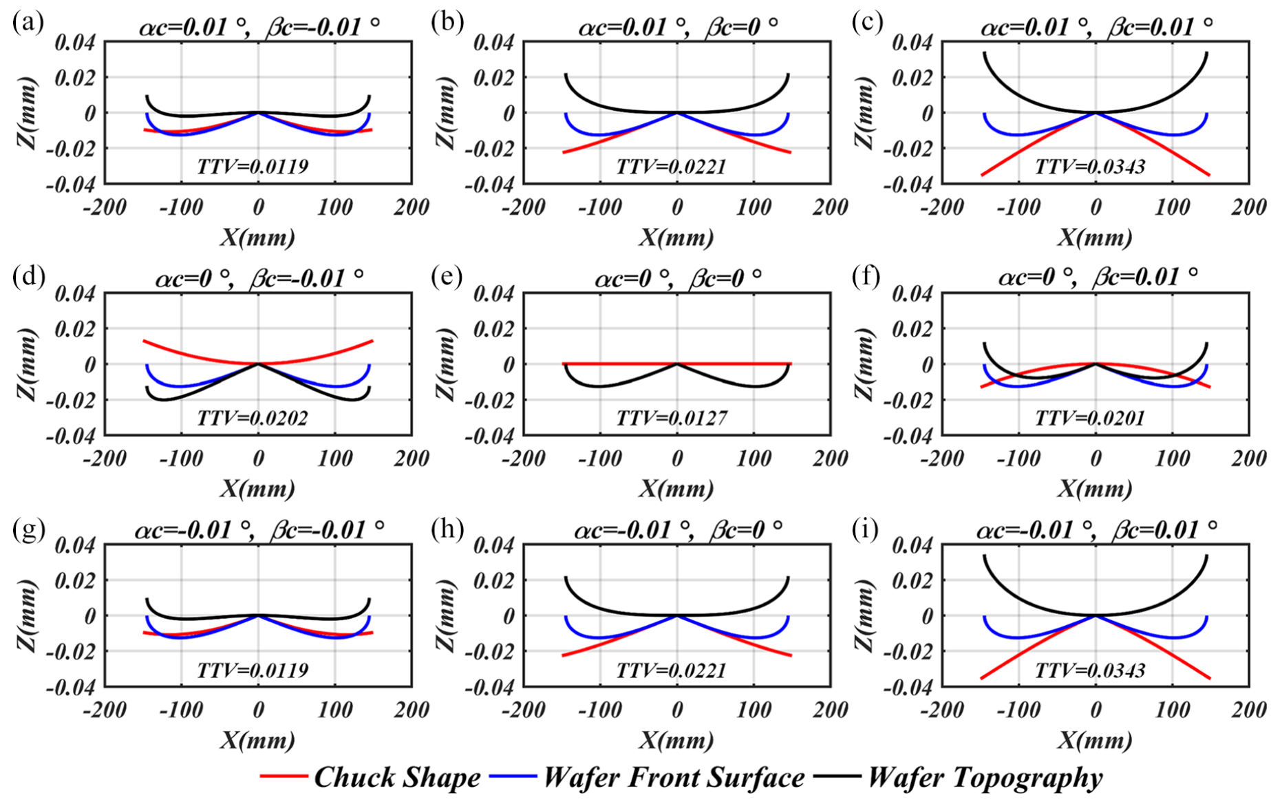
The topography of wafer in BGWOR under α W = 0.01°, β W = 0°: a) α C = 0.01°, β C = −0.01°; b) α C = 0.01°, β C = 0°; c) α C = 0.01°, β C = 0.01°; d) α C = 0°, β C = −0.01°; e) α C = 0°, β C = 0°; f) α C = 0°, β C = 0.01°; g) α C = −0.01°, β C = −0.01°; h) α C = −0.01°, β C = 0°; i) α C = −0.01°, β = 0.01°.

The topography of wafer in BGWOR under α W = 0.01°, β W = 0.01°: a) α C = 0.01°, β C = −0.01°; b) α C = 0.01°, β C = 0°; c) α C = 0.01°, β C = 0.01°; d) α C = 0°, β C = −0.01°; e) α C = 0°, β C = 0°; f) α C = 0°, β C = 0.01°; g) α C = −0.01°, β C = −0.01°; h) α C = −0.01°, β C = 0°; i) α C = −0.01°, β = 0.01°.
The simulation results in Figures 7 and 8 have some similarities. (1) No matter how much the dressing grinding wheel inclination is, the wafer thickness is uneven (TTV ≠ 0). The thickness at the edge of the wafer increases sharply but tends to flatten out as β C decreases. (2) When α C ≠ 0°, if βC remains constant, the wafer topography and TTV of BGWOR with the same absolute value of α C are also the same. (3) The overall effect of α C on wafer topography is greater than that of β C .
There are also some differences between the simulation results in Figures 7 and 8. When αW = 0.01° and βW = 0° and αC is a non-zero constant, the smaller the βC and more uniform the radial thickness of the wafer in BGWOR will be. When αW = 0.01° and βW = 0.01° and αC is a non-zero constant, the smaller the absolute value of βC and more uniform the radial thickness of the wafer in BGWOR will be.
The simulation under different radius of dressing grinding wheel
Similarly, MATLAB is used in this section to simulate the dressing surface of the chuck, the two-dimensional shape of the upper surface of the wafer in BGWOR, the wafer thickness t, and TTV under different dressing wheel radii. The effect of the radius of the dressing grinding wheel on the surface shape of the wafer in BGWOR was analyzed.
In the simulation parameters, the inclination angles of the dressing grinding wheel and the BGWOR grinding wheel are selected as the three groups with the minimum TTV in the simulation of the last section. The first group (a) consists of α W = 0.01°, β W = 0.01°, α C = 0.01°, and β C = 0°. The second group (b) consists of α W = 0.01°, β W = 0.01°, α C = 0.01°, and β C = 0.01°. The third group (c) have α W = 0.01°, β W = 0°, αC = 0.01°, and β C = −0.01°. The radius of the dressing grinding wheel in the simulation is 210, 150, and 80 mm respectively. The other simulation parameters are consistent with the parameters of the wafer shape under different inclination angles of the dressing grinding wheel. Similarly, the theoretical thickness of the wafer t0 is 0 mm. The simulation results are shown in Figure 9.

Simulation results of the topography of wafer in BGWOR: (a) α W = 0.01°, β W = 0.01°, α C = 0.01°, β C = 0°, (b) α W = 0.01°, β W = 0.01°, α C = 0.01°, β C = 0.01°, and (c) α W = 0.01°, β W = 0°, α C = 0.01°, β C = −0.01°.
Under different inclination angles of the dressing grinding wheel and BGWOR grinding wheel, the influence of different dressing wheel radii on the topography of the wafer has some similarities. Under the selected inclination angles of the dressing grinding wheel and BGWOR grinding wheel, it is difficult to adjust the radius of the dressing grinding wheel to make the wafer thickness uniform (TTV ≠ 0). The thickness at the edge of the wafer also increases sharply but tends to flatten with the increase of the radius of the dressing grinding wheel.
There are also some differences in the simulation results. When α W = 0.01°, β W = 0.01°, α C = 0.01°, and β C = 0° the TTV of the ground wafer increases with the decrease of the radius of the dressing grinding wheel. When α W = 0.01°, β W = 0.01°, α C = 0.01°, and β C = 0.01° the TTV of the wafer increases first and then decreases with the decrease of the radius of the dressing grinding wheel. When α W = 0.01°, β W = 0°, α C = 0.01°, and β C = −0.01° the TTV of the wafer decreases first and then increases with the decrease of the radius of the dressing grinding wheel.
Experimental verification
As shown in Figure 10, the angle of the grinding wheel shaft can be determined by adjusting the height of three points (A, O, B), which are located on the workpiece (chuck or wafer). RW in the figure is the radius of the workpiece. L is the center distance between the grinding wheel and the workpiece. The circle with a diameter of Rm is the position of the tip of the displacement sensor pointer in Figure 11. The height of the three points (A, O, B) is defined as ZA, ZO, ZB. The angles of the grinding wheel about the X-axis and the Y-axis are defined as α and β. The relation between α, β and ZA, ZO, ZB is as follows 4 :

Where

Illustration of relationship between α, β and ZA, ZO, ZB.

Angle adjustment of grinding wheel shaft.
Grinding experiments were carried out on a super precision wafer grinder (GP300, Dalian University of Technology), as shown in Figure 11. In these experiments, a dressing grinding wheel with a diameter of 300 mm and a BGWOR grinding wheel with a diameter of 145 mm were used. These two grinding wheels were resin-bond diamond grinding wheels with a grain size of #200 and #6000 respectively. The etched monocrystalline silicon wafers (100) and chuck with a diameter of 300 mm were also used in the experiments. In all the grinding experiments, the material removal depth was 100 μm, and all of them were carried out under the condition of 20°C deionized water cooling. The spark-out time was set at 5 s. The experimental parameters were NSW = 2400 r/min, NW = 120 r/min, fW = 20 μm/min, α w = 0.0151°, β W = 0.0015°, NSC = 2400 r/min, NC = 120 r/min, and fC = 10 μm/min. And the angles of the dressing grinding wheel, α C and β C , were measured after adjustment.
After the experiment, the flatness-measuring device was used to measure the dressing shape of the chuck and the upper surface of the wafer. The device was made of a trestle, high-precision displacement sensor (GT2-S5), and so on, as shown in Figure 12(b). The trestle had three legs and multiple holes for installing the displacement sensor. At the radial positions of 20, 40, 60, 80, 100, 120, and 140 mm, the height of the upper surface of the ground wafer and chuck, ZC and ZW, was measured relative to their respective centers. From the measured values, the thickness of the ground wafer at the measured point could be obtained. In addition, the height of the three legs should be recorded by an ideal plate afore the measurement of each position, as shown in Figure 12(a).
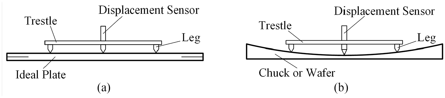
Principle of the wafer flatness measurement: a) The record of the height of three legs; b) Measurement of actual flatness of chuck or wafer.
Multiple measurements are made in different directions at each radial measurement position, and the average value is taken as the final measurement value. The comparison between the measured results and the simulation results is shown in Figure 13. The maximum error of the mathematical model and simulation is 4 μm, and most errors are less than 2 μm. The comparison shows that the actual measured values are in good agreement with the predicted values, although the measured data points are scattering in an acceptable range.

The comparison between the experimental results and the simulation results of the topography of ground wafer in BGWOR under different inclination angles of dressing grinding wheel: a) α C = 0.0141°, β C = 0.0039°; b) α C = 0.0106°, β C = -0.0015°; c) α C = 0.0073°, β C = -0.0065°.
Conclusions
In a word, the theoretical model of the wafer topography in BGWOR was established in this paper. Then the influence of the angle and radius of the dressing wheel on the topography of the ground wafer was analyzed by computer simulation. In the research, the main conclusions are as follows:
When the radius and inclination of BGWOR grinding wheel and the radius of dressing grinding wheel are constant, it is difficult to make the ground wafer flat by changing the inclination angles of the dressing grinding wheel. The thickness and TTV of the wafer are mainly determined by the inclination of the dressing grinding wheel. The overall effect of αC on wafer topography is greater than that of βC.
Under the selected inclination angles of dressing grinding wheel and the radius and inclination of BGWOR grinding wheel, it is difficult to adjust the radius of the dressing grinding wheel to make the wafer thickness uniform (TTV = 0). The thickness and TTV of the wafer are mainly determined by the radius of the dressing grinding wheel.
When the upper surface shape of the ground wafer in BGWOR is different, the influence of the inclination angle and radius of the dressing grinding wheel on the TTV of the wafer might be different. So in the actual grinding, the simulation analysis should be carried out according to the used grinding parameters.
Footnotes
Handling Editor: Chenhui Liang
Declaration of conflicting interests
The author(s) declared no potential conflicts of interest with respect to the research, authorship, and/or publication of this article.
Funding
The author(s) disclosed receipt of the following financial support for the research, authorship, and/or publication of this article: The authors acknowledge the financial support from the National Natural Science Foundation of China (Grant No. 51991372) and Liaoning Revitalization Talents Program (Grant No. XLYC2007049).