
Abstract
A rapid prototyping technique is demonstrated which uses a red femtosecond laser to produce a metallic mould which is then directly used for the replica moulding of PDMS. The manufacturing process can be completed in less than 6 h making it a viable technique for testing new designs quickly. The technique is validated by creating a microfluidic device with channels of height and depth of 300 µm, with a ramp test structure where the height and width of the channels reduces to 100 µm to demonstrate the techniques 3D capabilities. The resulting PDMS device was easily removed from the metallic mould and closely replicated the shape aside the expected shrinkage during thermal curing. As the technique uses a single replica process, the surface roughness at the base of the channels corresponds to the un-ablated polished metal mould, resulting in a very low surface roughness of 0.361 nm. The ablated metallic mould surface corresponds to the top of the PDMS device, which is bonded to glass and does not affect the flow within the channels, reducing the need for optimisation of laser parameters. Finally, the device is validated by demonstrating laminar flow with the no-slip condition.
Introduction
Manufacturing of microfluidic devices is performed using a variety of lithography methods including photolithography and soft lithography. Photolithography allows for patterning of features with a high resolution (1 µm under standard conditions), however it requires expensive equipment, a clean room, training and often hazardous substances. Soft lithography is a technique where elastomeric stamps or moulds are used to generate the desired features on a substrate. 1 This method also allows for high resolution (down to 30 nm), however the manufacturing of the initial elastomeric stamp/mould requires microlithographic methods (either photolithography or micromachining). Usually, elastomeric stamps are made from polydimethylsiloxane (PDMS) or polymethylmethacrylate (PMMA). PDMS has gained significant interest in the scientific field not only for the manufacturing via soft lithography but also as the final material in microfluidic devices. PDMS has many desirable properties for use in microfluidics, such as inertness, biocompatibility (non-toxicity), porous to allow oxygen to diffuse through for live cells, optical transparency (at 230–700 nm), flexibility and stability at a wide range of temperatures.2–4 It is also cheap, and many manufacturing methods allow for rapid prototyping using PDMS: making it very suitable for the production of low cost, single use (disposable) devices required for research. There are, however, some disadvantages associated with PDMS particularly within the biomedical field such as evaporation occurring within the channels leading to air bubble propagation which can lead to cell death or the high absorption of hydrophobic compounds however these problems can be mitigated through the use of certain surface coatings (such as parylene to prevent absorption) or environment control (such as humidifying the environment to prevent evaporation). 5
Replica moulding is a well-established technique for producing microfluidic devices, which is low cost and requires little specialist equipment.6–8 It involves pouring unpolymerised PDMS and a curing agent onto a mould and thermally curing the PDMS in an oven. The cured PDMS can then be peeled from the mould to give the microfluidic device. A clean room environment is not required and the equipment is cheap. The mould used for the fabrication of the microfluidics device is usually made from Su-8 or PDMS which is in-turn produced using conventional (and expensive) photolithographic techniques. There has also, however, been more interest in the direct writing of PDMS utilising laser engraving as opposed to utilising photolithographic techniques. 9 In recent years there has been increasing interest in using metal as the mould for the replica moulding of PDMS. Metallic moulds have advantages over conventional material moulds; as they can withstand the high temperatures with little expansion during thermal curing due to low thermal coefficients of expansion and can be re-used many times. 10 Demoulding of PDMS from metallic moulds has also been performed successfully without the need for surface coatings, further increasing the appeal of metallic moulds.11–13
The use of lasers for the manufacture of metallic moulds has become increasingly popular in recent years. Laser ablation is a non-contact process and can achieve high resolution geometries, limited by the beam spot diameter of the laser optics system. Three main types of lasers can be used: continuous wave, pulsed (nanosecond) or ultra-fast pulsed (femtosecond). 14 Pulsed lasers can give high quality ablation after optimisation of laser optical parameters, which has been widely researched.15,16 Ultra-fast lasers give the highest quality of surrounding material, due to the laser pulse duration being smaller than the electron cooling time (and lattice heating time) of the material, resulting in the material removal via sublimation rather than more conventional melting and vaporisation. 17
Currently, the manufacture of microfluidic devices is often costly, complicated, can take a long time and generally requires a lot of training. A comparison of some of the features for microfluidic device mould manufacture is shown in Table 1.

Additional to Table 1, optimisations of these various techniques have been researched such as with micromilled channels with gas-blowing assisted PDMS coating which allows for 3D planar surfaces to be manufactured and then optimising the surface by coating it with PDMS however this has only been researched for 100–800 um. 30 Additional full 3D techniques have also been explored such as the development of three-dimensional microfluidic mixers in glass by femtosecond laser direct writing or other 3D microstructures which are suspended inside fused glass or silica however these techniques don’t seem to be suitable for mould manufacture and only generate a single prototype for usage so to create more devices the initial manufacturing must be performed again.31–34 Laser ablation for moulds has also been discussed previously by Isiksacan et al. 35 however the devices manufactured would require several steps to achieve 3D planar surfaces as the ablation was a through-cut of sacrificial PDMS and acetate. From Table 1, a comparison can be made between each of the manufacturing processes to determine the niche where laser ablation lies.
From Table 2 it can be seen that laser ablation should be used for research prototyping due to the low commercial availability and for those researchers with access to laser facilities as an alternative for outsourcing their manufacturing. The other advantage of this is the relatively low operational costs so researchers entering the field of microfluidics can begin developing designs immediately with a relatively quick manufacturing time. The technology itself is suitable for chip designs with 3D geometries where small features may still be required and developed as seen in our test structure developed below. Finally, due to the laser ablation technique developing a mould, this allows for the development of chips that can be tested in biomedical applications where cleaning the chip is not suitable between each experiment. This therefore allows multiple chips to be developed cheaply using PDMS as prototype testing for developing research microfluidic designs.
A comparative summary of each of the manufacturing processes based on Table 1.

Our group proposes a rapid prototyping method which is comparatively fast and simple, as shown from Tables 1 to 2, making it more accessible for research groups who have access to laser facilities as well as offering the option of creating 3D moulds for more complex designs. The method should produce microfluidic devices which can be used for many different applications, from cell manipulation to fluid mixing, or bio-medical reactions (such as DNA micro-arrays) and for our own research, developing microfluidic devices in the field of biological cell injection.
Within this paper, a novel manufacturing method is demonstrated for the rapid prototyping of microfluidic devices with 3D structures using a metallic mould, and the subsequent produced device is analysed using the surface roughness of the channels and the geometric difference between the mould and final device is shown. To demonstrate that the manufacturing method can produce devices which are suitable for microfluidic applications, the device is tested to evaluate its capability of maintaining laminar flow within the channels.
Proposed methodology
Mould manufacture
The proposed method is fast, and requires only three pieces of specialist equipment; a femtosecond laser, a vacuum pump and an oven. To the best of our knowledge, this direct replica moulding technique of PDMS using a femtosecond laser is novel and can be used in the future for rapid prototyping of microfluidic devices.
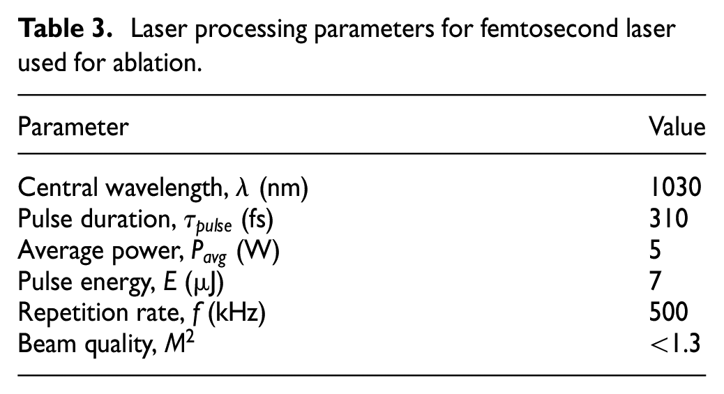
Commercially available 430 grade ferritic stainless steel was used as the material for the metallic moulds. Disks of 50 mm diameter were machined out of plates of thickness 0.7 mm and surface roughness of Sa = 0.197 µm. A femtosecond pulsed laser (Satsuma from Amplitude Systemes) was used to micro-machine the microfluidic channels (Lasea Multi-Axis Micro Machining Centre). The technical parameters of the laser source are listed in Table 3.
Laser processing parameters for femtosecond laser used for ablation.
The laser delivery system included a quarter wave plate to convert the s-type linear polarised beam to a circular polarised beam. The beam then passes through a beam expander and is fed into the Galvo-scanner head (RhoTHor RTA). The Galvo-Scanner head includes a telecentric lens and directs the beam onto the sample’s surface. The laser spot was Gaussian-shaped with spot diameter 2ωo = 5 µm in the focal plane. Assuming M2 of 1.3, the Rayleigh length ZR of the beam can be estimated to be 0.55 mm using,

where ωo is the beam radius, λ is the wavelength and M2 is the beam quality of the laser. The microfluidic device was designed in SolidWorks CAD software to have a main channel height and depth of 300 µm with a 3D geometry generated of a ramp which reduces uniformly in height and width to 100 µm to demonstrate the effectiveness of laser manufacturing 3D structures on metallic moulds as shown in Figure 1.

(a) CAD model of a test microfluidic device with channel heights and widths of 300 µm, (b) 3D test structure showing a ramp reduction in height to 100 µm and step back up to 300 µm and (c) top down view of the 3D test structure showing decreasing width to 100 µm.
The model shown in Figure 1 highlights all geometric shapes that could be expected in a microfluidic device as well as being able to highlight the 3D capabilities of the device. The CAD model was sliced using the ArtCAM software from AUTOCAD, and machine code generated using the laser control software Kyla. The scanning strategy used was Raster Mode scanning with 4 lines at 45° angles in each layer, with no contouring of the geometry. The hatch distance between each line was 4 µm giving a lateral overlap for each pulse of 31 µm. The scanning speed, v, was 750 mm/s, meaning a pulse separation, d, of 1.5 µm, which was calculated using equation (2)

With f being the repetition rate. 300 layers were required to give a final depth of 300 µm. As the depth of the sample (0.3 mm) is smaller than the calculated Rayleigh length, the focal point of the laser was kept constant for all layers. The lasing was performed at room temperature and atmospheric pressure with an extractor fan removing debris during ablation. The laser processing job took 150 min to complete and a negative mould of the device was made as shown in Figure 2.

View of the stainless steel negative mould for the manufacture of the PDMS channels.
Device manufacture
The PDMS (SYLGARD® 184, Dow Corning, MI) was prepared as described by the steps in Figure 3.

Step by step procedure of the manufacture of the PDMS device. Step 1: The mould is fabricated using the femtosecond laser as described above. Step 2: PDMS is prepared by mixing in a 10:1 ratio as recommended by the manufacturer and left to sit. Step 3: PDMS is poured onto the device, vacuumed, thermally cured and then peeled. Step 4: PDMS is bonded to the glass using PDMS as glue then cured for the final device.
Before step 4 in Figure 3 excess PDMS is cut off and channel openings were made using a Whatman Uni-Core 2.00 mm Punch and then cleaned and dried with ethanol. Due to the low weight of the device and small film thickness, the thin layer of PDMS mixture did not squeeze into the channels as no pressure was required to stick the device to the glass slide. The whole process can be completed in less than 6 h. About 1 h is required for laser system setup, 2.5 h for the mould fabrication via laser ablation, 1.5 h for PDMS preparation and device manufacture via thermal curing and 1 h for sealing the device to a glass plate using PDMS and thermal bonding.
Device testing
Typical methods to measure the flow velocity within channels include particle image velocimetry, hot wire anemometry or pressure probes.36–38 Particle image 8 velocimetry is an indirect, non-intrusive technique which uses tracer particles within flow to determine flow velocity and can be applied to micro-geometries. Typically, tracer particles for use in microfluidic devices are small (on the nanoscale) spherical fluorescent beads, and their motion is recorded using epifluorescence microscopes and other optical equipment. 39 In this report, a simplified version of particle image velocimetry is performed using food dye and a high frame rate camera. The aim is to demonstrate that the channels can maintain laminar flow, which is a requirement for most microfluidic devices. This can be done by calculating the maximum flow velocity within the channels and comparing it to theoretical laminar results.
The device was filled with de-ionised water by attaching a syringe to tubing with an outer diameter of 2 mm which was then inserted into one of the inlets of the device. Another syringe was filled with red food colouring and placed in a World Precision Instruments syringe pump, and then connected to the device using tubing. The device was placed in a petri-dish on a BestScope BS-2090 inverted microscope, equipped with a x0.45 Basler 106752 Camera set to record at 200 frames per second (fps). The syringe pump was used to deliver the dye into the water filled device to estimate the velocity of the water within the channels. Footage was recorded for volumetric flow rates ranging from 0.04 to 0.3 ml/min, between each flow rate reading the device was flushed thoroughly with de-ionised water to remove the dye. The testing was performed at room temperature (19°C) and the set up can be seen in Figure 4.

(a) Syringe pump to apply constant fluid flow to the device and (b) the microfluidic device under a microscope.
Results and discussion
Analysis of mould and device
The metallic mould and fabricated PDMS device were analysed using an Alicona G4 InfiniteFocus (IF) system to obtain surface roughness and surface profile measurements. Surface roughness measurements were taken in two places on both the device and mould: i) the top surface of the device, corresponding to the ablated metal of the mould and ii) the bottom of the channels of the device, corresponding to the polished metal of the mould. The surface roughness values are shown in Table 4.
Surface roughness (Sa) values for the mould and device at specific locations.

Similar to the technique performed by the surface roughness at the base of the channels is similar to the surface roughness of the initial polished metal disk. 40 This leads to low surface roughness in the channels of the final device, reducing friction and aiding laminar flow. This also allows the possibility to easily change the surface roughness of the channels, by selecting an initial metal substrate with the desired surface roughness. The surface roughness at the top of the device (corresponding to the ablated metal) is higher, at 3.496 and 2.625 µm for the PDMS and metal mould, respectively. However due to the top-lid design of the microfluidic device, it is thermally bonded to a glass slide and does not affect the flow within the device. This is advantageous as it means that the resulting surface roughness produced by the laser ablation does not need to be greatly optimised as it has little effect on the functionality of the device. The surface roughness has increased by 60.4% and 30.2% from the metal to the PDMS for the top surface and bottom of channel respectively. Profile cross sections of the channel were measured using the Alicona System at locations A and B shown in Figure 5.
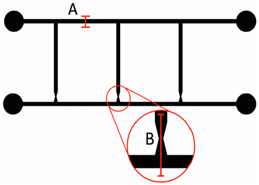
Surface profile measurement cross section locations for the device. ‘A’ corresponding to the general channel cross section. ‘B’ corresponding to the longitudinal cross section of the 3D test structure.
Cross section A shows the general cross section of the channel measured and is shown in Figure 6(a). The general shape of the resulting channel in both metal and PDMS shows a narrow bottom, opening up to a wider entrance. This change from narrow to wider side walls is caused by tapering of the laser ablation as it progresses further into the metal. Beam reflection and energy absorption occurs on the side walls and the beam can self-focus in the plasma generated, leading to a lower laser power on the sample. This reduces the fluence of the laser contacting the surface and results in poorer ablation. This effect has been widely researched and can be reduced by varying the optical parameters, such as the laser fluence, or depth of focus (Rayleigh Length) of the laser source. 41

(a) Cross section of channels at location (A) from Figure 5 for the metal mould and PDMS device. The PDMS and metal were aligned with their datums set at a height of 0 µm at the bottom of the channels when taking measurements and (b) the root mean squared (RMS) deviations in the y direction (height) between the desired shape, metal and PDMS at different locations. NB: the bottom location has been truncated 30 µm on either side, to remove the large errors at the walls of the channels to give a representative RMS along the bottom of the channel.
The metallic mould shows maximum undershoots of 42 µm (Figure 6(a)) at the edges of the channels, which are also replicated in the PDMS, to a lesser extent of 30 µm due to the shrinkage of the PDMS during thermal curing. These undershoots border all channel edges, which can be seen more clearly in Figure 7(b) and are due to the raster scanning strategy of the laser. The laser decelerates then accelerates at the channel edges to change direction and start a new line in the raster scanning mode. This results in more pulses of the laser reaching the surface at these points and hence more ablation occurs at the edges of the channels. It is possible to optimise the scanning strategy to avoid these edge effects, by adding ‘off times’ to the laser during deceleration and direction changes, or by using PID controllers to minimise the errors in the galvanometer’s movement. 42 A standalone software tool has been developed in recent years which causes adjustments to the beam path to avoid effects caused by the difference in the desired and actual beam path due to acceleration and deceleration of the beam. 43 The use of this software would reduce to overshoot effects seen in our sample.
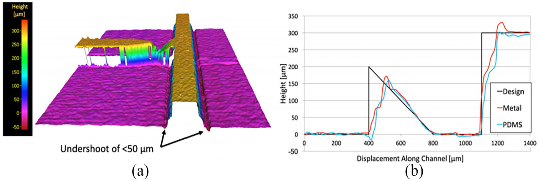
(a) 3D height profile of metal mould of the channels including the 3D test structure and (b) longitudinal cross section B of 3D test structure for metal mould and PDMS (see Figure 5).
The Root Mean Squared (RMS) deviation of the height of the metal and PDMS compared to the design height are calculated in MATLAB 2017a and shown in Figure 6(b). These have been calculated on the left, right, bottom and across the whole of the profile. Due to shrinkage of the PDMS during thermal curing, higher RMS values are seen for PDMS than the metal when compared to the design. The RMS for metal and PDMS at the top of the channels is large (41.9–52.7 µm and 47.5–60.4 µm, respectively), due to the aforementioned tapering and undershoots. To obtain a true RMS for the bottom of the channel, the results were truncated by −30 µm on either side of the channel walls to remove the large errors seen on the channel walls. Here we see small RMS values (1.68 µm and 6.3 µm respectively) compared to the desired shape. In total across the channel profile, the RMS for metal and PDMS is 42.9 and 49.3 µm, respectively, which, though large, it is clear that with laser parameter optimisation these RMS values can be greatly improved.
The RMS is also calculated between the metal and PDMS to evaluate the changes in the PDMS during curing. Across the channel profile, the total RMS between the metal and the PDMS is 18.8 µm, due to shrinkage during thermal curing. PDMS shrinkage has widely been researched and is affected by the ratio of curing agent to elastomer base and the curing temperature and time. 7 Using the calculated RMS (or expected % shrinkage of PDMS from tables), the metal mould can be re-designed to negate the effects of the shrinkage and hence better replicate the desired geometry.
The 3D test structure in the channels is also examined. Figure 7(a) shows a 3D height profile of the metallic mould at the restriction and the cross section of the change in height of the channels across the restriction (B in Figure 5). The horizontal accuracy of the metallic mould and resulting PDMS at the base of the channels (height 0 µm) is good, with the test structure starting and ending within ±20 µm of the correct location. The tip of the structure is intended to be a vertical surface reaching to 200 µm however the metal and PDMS have failed to do this. The metal mould has undershot the height by 28 µm and has a horizontal error of 110 µm, and the PDMS closely replicates this with errors of 40 and 122 µm, respectively. These large errors are due to the minor level of optimisation of the laser parameters and scanning strategy, and could be improved as discussed previously. However, the resulting PDMS device has successfully replicated 3D structures within the micro-channels.
Laminar flow
The transition from laminar to turbulent flow in channels typically occurs at Reynolds numbers over 2000. The maximum flow velocity within our channels for laminar flow can be calculated using equation (3):

Where ρ is the density of the fluid, u is the average fluid velocity, µ is the dynamic viscosity of the fluid and Dh is the hydraulic diameter of the channel which for rectangular channels is calculated as
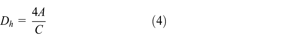
Where A is the cross-sectional area of the channel and C is the wetted perimeter of the channel. This yields a maximum mean inlet velocity of 7.02 m/s. For laminar flow driven by a constant pressure gradient, P, the velocity profile of subsequent laminar flow can be calculated using the well-known Hagen–Poiseuille equation. This can be modified for use in rectangular channels with widths

The volumetric flow rate (Q) can be calculated by integrating over the velocity profile yielding
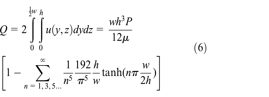
By rearranging equation (6) and using the known volumetric flow rate of the fluid the pressure gradient across the channel can be calculated in MATLAB 2017a up to terms n = 20 (higher values only change the eighth decimal place). Using this value, the velocity profile is calculated using equation (5) where the terms converge again at approximately n = 20. The generated velocity profile for a volumetric flow rate of 0.15 ml/min can be seen in Figure 8 and shows a parabolic profile with a maximum peak velocity of 58.2 mm/s and no-slip condition at the channel walls.

(a) 3D and (b) 2D theoretical velocity profile for volumetric flow rate of 0.15 ml/min for laminar flow for channels of height and width of 300 µm based on equation (5).
By analysing the recorded footage of the fluid within the channels, the peak velocity of the dye within the channels can be estimated. This was done by measuring the number of frames required for the peak of the dye flow to cover a measured distance and using the known fps of the footage, and can be seen in Figure 9. For lower volumetric flow rates, the dye flow profile was parabolic, and demonstrated the no-slip condition at the channel walls where the dye progressed very little compared to the peak of the flow. The flow also appears un-disturbed and is not showing any turbulence or eddies. For higher flow rates the dye flow profile is much more elongated and irregular (see Figure 9(b)), however there are not any vortexes and still the flow still appears to have straight flow lines, as expected for laminar flow.

Images of the recorded footage of dye flow in the channels: (a) volumetric flow rate of 0.06 ml/min shows a good parabolic flow profile and no-slip condition of the dye at the channel edges and (b) volumetric flow rate of 0.2 ml/min shows a stretched dye profile which is irregular and pointy.
The maximum velocity of the dye flow is calculated for each of the volumetric flow rates and plotted with the theoretical maximum velocities in Figure 10. A least squares fit has been plotted for the measured data points and has an R2 of 0.95 showing a strong linear correlation. The experimental results consistently underestimate the maximum flow velocity in the channels which can be attributed to systematic errors such as the channels being larger than the dimensions used in theoretical ones used (see Figure 6(a)) which reduces the flow rate. Another reason could be due to the different sizes of particles of the dye causing it to move slower than the fluid is as it is reliant on the drag force.
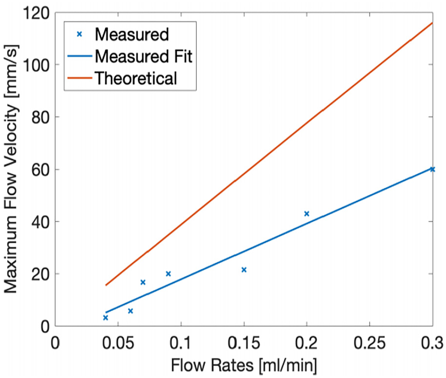
Theoretical and measured maximum velocity of flow within the microchannels. A least squares fit has been plotted for the measured results with an R2 value of 0.95.
In summary, although the results are under-estimating the maximum flow velocity within the channels, the flow profile is laminar due to the parabolic flow shown at lower flow rates, a similar increase in maximum flow velocities for each flow rate and demonstrates the no-slip condition at the channel walls. For higher flow rates, the flow is still laminar due to the lack of vortices and conical, albeit elongated, flow profile demonstrated. This confirms the manufacturing techniques ability to produce channels which can sustain laminar flow. In addition, the produced device remained fully sealed for the entirety of testing which included flushing with de-ionised water and dye over 50 times reflecting the viability and durability of using uncured PDMS for sealing rather than the conventional plasma bonding.
Conclusion
A novel rapid prototyping technique for the production of microfluidic devices using a red femtosecond laser was successfully demonstrated. This new method offers a quick way for researchers to generate a microfluidic mould quickly if they have access to laser ablation facilities but not traditional microfluidic manufacturing. The produced device showed low surface roughness at the base of the channels due to the inverse design of the metallic mould. Widening and overshoots at channel cross sections were observed and were attributed to low levels of laser parameter optimisation. A simplified form of particle image velocimetry was used to successfully demonstrate laminar flow within the channels validating the manufacturing method’s ability to create microfluidic channels. The quality of the produced device is greatly affected by the quality of the metallic mould. It is clear that with more optimisation of laser micro-processing by minimising impact of the raster scanning for better replication of 3D features, optimising the laser fluence for minimised tapering of the channel walls and implementing sharper laser movement control, this manufacturing technique could be used to create high quality microfluidic devices.
Footnotes
Acknowledgements
The authors wish to thank with appreciation the laser-based manufacturing research group within the Advanced [M]anufacturing Technology Centre, Department of Mechanical Engineering, University of Birmingham, for the support provided in the manufacturing realisation aspects of this research.
Handling editor: James Baldwin
Declaration of conflicting interests
The author(s) declared no potential conflicts of interest with respect to the research, authorship, and/or publication of this article.
Funding
The author(s) received no financial support for the research, authorship, and/or publication of this article.