
Abstract
This study proposes a method to improve the manufacturing process of a surface anchor structure for the injection molding along with bonding properties of the plating layer for antennas, which can be applied to the Laser Direct Plating (LDP) process for the production of a three-dimensional antenna integrated with a mobile device case. By adjusting parameters such as the output of the laser processing, scanning speed, and pulse recurrence frequency, a micro anchor structure was developed on the surface of the injection mold. The measurement of the surface roughness using a 3D surface profiler showed that the roughness improved by approximately 3.6 times, from 0.96 to 3.24 µm. In addition, the zigzag arrangement of the micro anchor structure was improved by 1.2 times compared to the even arrangement. Furthermore, if the micro anchor structure contained a wall after laser processing, the bonding strength of the plating solution was 69%; with no wall, it was 94% or higher. Thus, the existence of walls resulted in a difference of 1.4 times in the bonding strength. The laser processing improved the bonding strength of the plating solution on the micro anchor structure by approximately 19 times.
Keywords
Introduction
There has been continuous technical development of portable mobile devices toward being multifunctional, lightweight, and slim devices, and the importance of the detailed design of components to meet such functional requirements has been rising consistently. Particularly, smartphones and tablets, which are widely used, are advancing toward being multifunctional high-end portable devices that include the functions of a PC and exceed their original functionalities through the introduction of antennas that enable them to accommodate multiple wireless communication capabilities. Furthermore, smartphones contain five or more antennas, including the main (4-band or more antennas for 3G, 4G, and global roaming), GPS, Wi-Fi, BT, LTE, and sub-antenna, and since the antenna requirements are somewhat different for each country, the development directions depend on the requirements of each telecommunications company. 1 As the acquisition of sufficient space is essential for enabling appropriate performance of mobile device antennas, the use of antennas is considerably limited in device design. 2 Particularly, antennas that support multiband zones have a larger size. 3 The most mobile devices currently in the market support multiband zones considering global roaming. Accordingly, there has been significant demand for technical changes in the design and production of antennas that can facilitate the minimization of space and multiband support.4–7 Existing mobile antennas are produced in accordance with carrier type, but the corresponding method is limited not only in terms of reduction of manufacturing costs, processing time, and lightweight and compact device design, but also in responding to ergonomic demand, such as the curvature case design. Recently, there has been a growing interest in case-integrated antennas (where antennas are integrated into the rear case) and related manufacturing processes. 6 The most widely used methods for case-integrated mobile device antennas are the double injection molding process, 8 PDS (Printing Direct Structure),9,10 DPA (Direct Printing Antenna),11,12 and LPS (Laser Plating Structuring).13–15 These manufacturing technologies use different materials and have advantages and disadvantages. Although they facilitate the production of ultrathin, high-performance, multiband, and wideband antennas, the manufacturing costs are higher than those corresponding to existing manufacturing techniques, and reliability issues, such as the adhesion force under high temperature and high humidity, still exist. The double injection molding technique involves the injection of ABS (Acrylonitrile, Butadiene, Styrene) resin used for plating to produce antennas from the injection mold. Although it increases the effective area of the antenna and the manufacturing costs are low, it produces many defects during the molding process, and the design and manufacturing of antennas through this technique is still difficult. PDS involves printing metal ink (such as Cu) or plating resin ink on a concave elastic stamp/pad, which is then printed again on the object to plate the object, and the process reduction can save costs and development time. Furthermore, it reduces the assembly process and sample production period as well as injection molding costs owing to reduction in the number of parts. However, commercializing it is still difficult as the issue of the bonding strength of the case-integrated antenna to the injection mold has not been solved completely, and the plating fault rate is still very high. The Laser Direct Structuring (LDS) 16 activates the resin surface and secures the seed surface for the electro less plating17,18 by irradiating the laser on the case with metal additives in the required circuit pattern. In this technique, the volume of the special resin used is small, and despite the long plating process due to the use of barrel chemical plating, it can plate a considerable number of antennas simultaneously. Therefore, it is widely used in the manufacturing of carrier-type antennas. Because of the complex metalizing process and susceptibility of the plate on impact, many studies have attempted to find alternative methods to LDS; recently developed alternatives include DPA and LPS. DPA enables direct printing on the case-integrated antenna component by mixing metal and special ink, and thus it could function like a metal plate. Although the resulting antenna is robust against drops and the DPA reduces the failure rate drastically, the bonding force between the case and antenna is low and the printing precision is limited. Furthermore, it does not reach an electrical conductivity up to 1 × 10⁻⁶ Ω·cm, which is the requirement for currently used inks (such as Ag); thus, it cannot be applied to case-integrated antennas as it cannot be applied to 780-MHz low-frequency LTE antennas. LPS produces antennas by electro less plating of ABS on the plate, converting butadiene into an electronic conductor (such as Pd) chemically, creating an island of the plated part in the designed shape using a laser, and electroplating the antenna. Although it can be applied to various types of resins and involves low manufacturing costs and short processing time, its process is complex as it requires both electro less plating and electroplating after spraying the plating solution on the plate. To overcome this shortcoming, many researchers are focusing on LDP, in which antenna structures are formed selectively on the laser-irradiated part through consecutive electro less and electroplating processes after selectively patterning the case surface with a laser and forming the micro-nano anchor structure with an undercut. Besides the low cost-high throughput process, LDP enables the realization of micro line-width patterns and low conductance that space-saving third generation antennas would require. Furthermore, it is considered a new case-integrated patterning technique as it enables the selective formation of 3D antennas; thus, it can effectively cope with the changes in design and function of wireless communication devices. Its impact is very high, as besides antennas, it can be used to manufacture alternative modules for mobile camera modules, LED plate integrated modules, automobile sensors, power devices like EBS/ESM, medical device harnesses, and so on. Some technical limitations of the existing LDP are the incompleteness of the laser etching process, pitch depth of the laser etching pattern, lack of Pd (palladium) activation, need for an additional wet-etching process, and insufficient laser etching precision of glass fiber-containing materials. To overcome these limitations, we used injection forming work-piece from PC (Polycarbonate) materials. This study proposed surface microstructure method and joint characteristics to enhance the plating properties of PC work-piece surfaces, which can be applied to the LDP process as shown in Figure 1.

Laser Direct Plating (LDP) process; (a) substrate(case), (b) laser ablation(islanding), (c) electro plating, and (d) electro less plating.
Production of the micro surface anchor structure
The micro surface anchor structure was constructed by laser processing on the surface of PC injection forming work-piece made with mold temperature of 70°C to 120°C and injection pressure of 1000∼1500 kg/cm2. The mathematical model of the structural shape for improving the bonding strength of the plating layer and injection forming work-piece is expressed by equation (1) 19 using the following parameters:

F = Bonding strength (kgf/cm)
Em = Young’s modulus of the adherend
a = Depth of the resin surface bonding (cm)
b = Width of the plating layer
tm = Thickness of the plating layer
KL = Force applied for pulling metal from one bonding D1/4
d = Distance between void and void
Here, the parameters to be controlled during the laser process are the depth of the void and the distance between void and void, which change according to the irradiation speed and output of the laser. Figure 2 shows an analysis of the surface characteristics before the laser processing on injection forming work-piece with 3D surface profiler and SEM. Figure 2(a) and (b) shows the 3D surface profiler measurement results the surface roughness was 7.33 µm, showed the characteristics of a relatively smooth surface. In addition, the results of the SEM scans in Figure 2(c) were not suitable for plating because the surface was smooth. So, to improve the efficiency of the plating, our produced anchor structures of micro-scale and nano-scale on the surface of the injection forming work-piece by varying the output of the laser, the pulse velocity, and the scanning speed

3D profile data and SEM image of injection forming workpiece surface before the laser processing; (a) 3D profile measurement result of PC work-piece surface (2D), (b) 3D profile measurement result of PC work-piece surface (3D), and (c) SEM image of PC work-piece surface.
Process properties in terms of laser output
The micro anchor structure of injection forming work-piece was created using MD-V9900A (KOREA KEYENCE Co., Ltd./maximum output power: 10 W) laser. First, to analyze the laser process properties in terms of laser output power (P), scanning speed (S/S), and pulse recurrence frequency (Q) were set to 2000 mm/s and 20 kHz, respectively, and the laser process was applied to the surface of the forming work-piece while changing the output (P) between 3 and 6 W. Figure 3 depicts the results of the laser process under output changes. As the output increases, the depth of the micro structure anchor shape increases from approximately 10.8 to 15.5 µm, and the diameter increases from approximately 47 to 59 µm. Further, as shown in Figure 4, the depth of the processed structure increased rapidly when the output was between 4 and 5 W, and after 5 W, its increase became gradual. The pattern size increased drastically when the output was between 3 and 4 W, and after 5 W, its increase rate became gradual. Furthermore, the wall between the processed structures drastically decreased when the output was between 3 and 5 W, but it became gradual after 5 W. The bonding strength given by equation (1) is proportional to a process depth to the power of quarter. As the output increased, the increase in process diameter was 27.7% and the increase in process depth was 47.6%. This indicates that to increase bonding strength, laser process at a higher output is desirable.
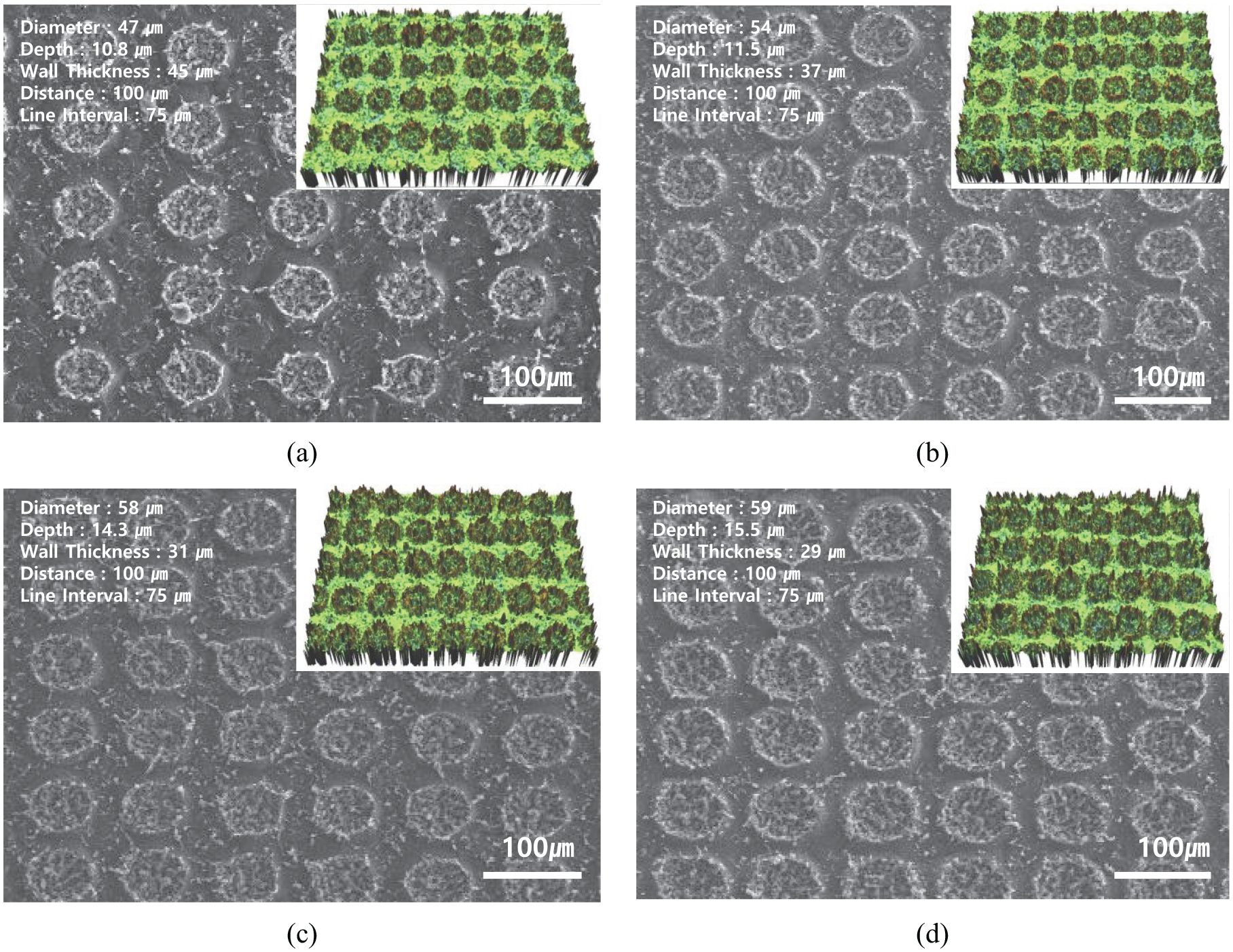
Characteristics of structural formation according to the change of laser output values (scanning speed: 2000 mm/s, pulse recurrence frequency: 20 kHz): (a) laser output power 3 W, (b) laser output power 4 W, (c) laser output power 5 W, and (d) laser output power 6 W.

Variation of the size of a microstructure according to changes in laser output value: (a) pattern to pattern distance, (b) microstructure depth, (c) microstructure diameter, and (d) microstructure wall thickness.
Process properties about the pulse recurrence frequency and scanning speed of the laser
To analyze the process properties based on the change in pulse recurrence frequency of the laser process, the output and scanning speed were set to 7 W and 2526 mm/s, respectively, and the process was performed while changing the pulse recurrence frequency between 26 and 28 kHz. Although pulse recurrence frequency has been reported to affect the depth of the processed structure, this condition was prevented because of the properties of the material (PC) used, as shown in Figure 5. However, it did have some effect on the diameter and arrangement between the processed structures. Nevertheless, no specific effect was observed.
Characteristics of structural formation according to the change of pulse recurrence frequency values (power: 7 W, scanning speed: 2526 mm/s): (a) pulse recurrence frequency: 26 kHz, (b) pulse recurrence frequency: 27 kHz, and (c) pulse recurrence frequency: 28 kHz.
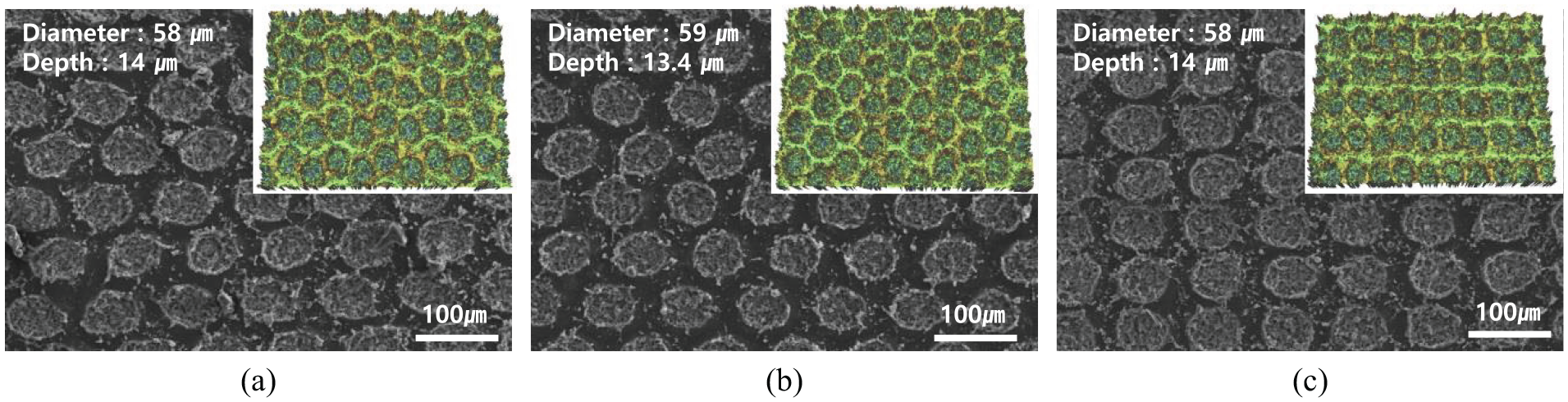
To analyze the process properties under a change in the scanning speed in the laser process, the output and pulse recurrence frequency were set to 9 W and 26 kHz, respectively, and the scanning speed was changed to 1500 and 2526 mm/s. Scanning speed is a parameter that can cause adverse effects on the surface, such as heat damage, and speed change is known to affect the formation of micro holes on the surface. 20 When the scanning speed is increased, it moves faster than the laser processing area, so overlapping parts are prevented. As shown in Figure 6(a), the processed structure with a scanning speed of 2526 mm/s was not overlapped, so that the unprocessed smooth surface between the structures caused a decrease in bonding strength. However, as shown in Figure 6(b), the processed structure with a scanning speed of 1500 mm/s was overlapped and wall did not exist between the structures. The surface consists of micro and nanolevel porous formations and was expected to improve the bonding strength between the plating layer and the injection forming work-piece.

Characteristics of structural formation according to the change of scanning speed values (power: 9 W, pulse recurrence frequency: 26 kHz): (a) scanning speed: 2526 mm/s, (b) scanning speed: 1500 mm/s.
The characteristics of the plating bonding according to the arrangement of patterns
By considering the surface structuring properties in terms of the laser process conditions, micro anchor structuring was realized in a 10 × 5 mm area of the surface of the injection forming work-piece under different laser conditions. Electroless plating was performed on the surface of the micro anchor structure produced. Finally, 1 h heat treatment process was performed at 80°C. The change in surface roughness with the change in the laser process conditions as well as the change in bonding strength with the electroless plating was verified. The bonding strength was measured by x-cut test. First, it uses a cutter knife to scratch the plated surface in the square shape of a 1.5 mm. Next, the bonding strength was measured by attaching a tape (3M #610) to the scratched surface, applying a pressure of 50 N, and then removing the tape. The surface roughness of the injection forming work-piece before the laser process was 0.96 µm, and the bonding strength of the plating was 5% or lower. Microlevel structures were implemented in uniform arrangement and zigzag arrangement.
Uniform pattern arrangement
First, Figure 7 were the SEM image of the surface shape and surface roughness measurements using a 3D surface profiler after the laser process. Figure 7(a) was the scanning speed was adjusted to 2526 mm/s so that there was no overlap of the structure and implemented as an array structure of a single micro-structure. Areas such as the blue circle are areas where laser processing is performed, and areas such as the red circle are areas where laser processing is not performed. The surface roughness after the laser process was 2.72 µm for the uniform arrangement, which was over 2.7 higher than that before the process. Further, it was observed that the bonding strength of the plating increased more than that in the area without the laser process, due to the microlevel structures produced on the surface of the injection forming work-piece and the hundreds of nanoscale holes. Under the condition where a wall of the microlevel structures exists, the plating area of the uniform arrangement was found to be approximately 49% through image processing. Figure 7(b) were the surface roughness and plating bonding strength were observed by producing a surface without the wall. This surface was obtained through the uniform arrangement of microlevel structures by adjusting the scanning speed to 1500 mm/s. The diameter and depth of the microlevel structure produced by the laser process were 36 and 13 µm, respectively. The surface roughness was 3.24 µm in the uniform arrangement, and upon removing the wall of the microlevel structure, the surface roughness increased by approximately 1.2 times, which was approximately 3.2 times higher than the surface roughness before the laser process.

Bonding characteristics of electroless plating of micro anchors with a uniform arrangement (power: 9 W): (a) scanning speed: 2526 mm/s, (b) scanning speed: 1500 mm/s.
Zigzag pattern arrangement
Figure 8 shows the SEM image of the surface shape and the surface roughness measurements obtained using a 3D surface profiler after the zigzag arrangement laser process. Figure 8(a) was the scanning speed was adjusted to 2526 mm/s so that there was no overlap of the structure and implemented as an array structure of a single micro-structure. The surface roughness after the laser process was 2.98 µm for the uniform arrangement, which was over 3 higher than that before the process. Under the condition where a wall of the microlevel structures exists, the plating area of the uniform arrangement was found to be approximately 69% through image processing. Figure 8(b) was the surface roughness and plating bonding strength were observed by producing a surface without the wall. This surface was obtained through the zigzag arrangement of microlevel structures by adjusting the scanning speed to 1500 mm/s. The microlevel structure size produced by the laser process was such as Figure 7(b). The surface roughness was 3.16 µm in the zigzag arrangement, and upon removing the wall of the microlevel structure, the surface roughness increased by approximately 1.1 times, which was approximately 3.2 times higher than the surface roughness before the laser process. Additionally, the surface with the microstructure wall affected the plating bonding strength, but the plating bonding strength of the surface without the wall was 94% or higher in both arrangements, showing that the structure arrangement had negligible effect on the surface roughness.

Bonding characteristics of electroless plating of micro anchors with zigzag arrangement (power: 9 W): (a) scanning speed: 2526 mm/s, (b) scanning speed: 1500 mm/s.
The characteristics of the plating bonding
Figure 9 shows the results of the plating bonding strength test according to the presence or absence of a wall after laser processing. Figure 9(a) shows the SEM image of a laser processed injection forming work-piece to allow the wall to exist. It shows that walls and unprocessed space exist. Figure 9(b) and (c) shows the results of the joint strength test after plating on a laser-processed surface so that the wall exists. The test results confirmed that the plating layer partially peels off. Figure 9(d) is a SEM image of a laser-processed injection forming work-piece without the wall. It shows that no wall exists on the surface and that porous of micro and nano-scale is formed. Figure 9(e) and (f) is the result of testing the bonding strength after plating on the laser processed surface without the wall. We can see that the plating is well bonded to the surface. When manufacturing mobile device case integral three-dimensional antennas, laser processing has high power and low scanning speed, and fabrication of surface microstructures with zigzag arrangement has improved the bonding characteristics of the plating.

The results of the plating bonding strength test according to the presence or absence of a wall after laser processing: (a) SEM image of a laser processed injection forming work-piece to allow the wall to exist, (b) real image of bonding test result to the presence of a wall after laser processing, (c) optical microscope image of bonding test result to the presence of a wall after laser processing, (d) SEM image of a laser-processed injection forming work-piece without the wall, (e) real image of bonding test result to the absence of a wall after laser processing, and (f) optical microscope image of bonding test result to the absence of a wall after laser processing.
Summary and conclusion
This study proposes a method to improve the manufacturing process of the micro anchor structure by injection forming work-piece and the bonding properties of the plating layer for antennas, which can be applied to LDP process for the production of a 3D antenna integrated with a mobile device case. The micro anchor structure of the surface of the injection forming work-piece was created by the laser process. Considering the effect of laser output on the process properties, the depth of the processed structure increased drastically when the output was between 4 and 5 W and its increase became gradual after 5 W; similarly, the pattern size increased drastically when the output was between 3 and 4 W and became gradual after 5 W. The wall between the processed structures decreased drastically when the output was between 3 and 5 W and became relatively gradual after 5 W, indicating that a high-output laser process was suitable for fabricating the micro anchor structure. In addition, considering laser pulse recurrence frequency and scanning speed, the change in the pulse recurrence frequency had a negligible effect on the processed structures, whereas with change in scanning speed, the processed structures were overlapped so that a wall with several microscale to hundreds of nanoscale holes between the structures was formed, improving the bonding strength with the plating layer. At a higher scanning speed, the wall existed in the processed structures, and the plating bonding strength was 49% in the even arrangement and 69% in the zigzag arrangement. At a low scanning speed, there was no wall between the processed structures, and the bonding strength was 94% or higher, regardless of the arrangement type. In this study, the bonding strength of the plating on the surface of the antenna injection forming work-piece before the laser process was 5% or lower, but after the laser process, it increased to 94% or higher. Thus, it was shown that the implementation of the LDP process, which provides approximately 19 times higher bonding strength of plating, would facilitate the manufacturing of a case-integrated antenna. If the proposed method is applied to the LDP process, the high electroless plating rate at 94% or higher in the selective area would provide higher energy efficiency and reduce plating solution loss compared to the electroplating method.
Footnotes
Handling Editor: James Baldwin
Declaration of conflicting interests
The author(s) declared no potential conflicts of interest with respect to the research, authorship, and/or publication of this article.
Funding
The author(s) disclosed receipt of the following financial support for the research, authorship, and/or publication of this article: this paper was supported by Korea Institute for Advancement of Technology (KIAT) grant funded by the Korea Government (MOTIE) (P0002092, The Competency Development Program for Industry Specialist) and the National Research Foundation of Korea (NRF) Grant funded by the Korean Government (MSIT) (No. 2015R1A5A1037668).