
Abstract
For exploring the mechanical properties and behaviors of new materials, a novel in situ nanoscratch device compatible with commercial microscope has been developed. The developed device with specific dimensions of 178 mm × 165 mm × 78 mm includes the coarse positioning module, the precise feed module, the measurement module, and the control module. Integrating the servo motor, worm and gears, ball screw, flexure hinge, and piezoelectric actuator, the device can realize macroscopical coarse positioning motion and precise feed motion. A novel arrangement of load sensor and indenter with no middle chain is used to reduce the measurement error. Closed-loop control system is established to guarantee the accuracy of load and displacement control. Mechanical properties of the developed device have been proved by calibrating the load sensor, finite element analysis of flexure hinge, and verifying the output performance. The in situ nanoscratch test has been conducted on the single crystal copper. The captured images and finite element analysis prove the feasibility and accuracy of the developed device.
Introduction
Currently, in view of the rapid development of the material preparation industry, more and more new materials emerge in endlessly. Indentation method has become a powerful lossless testing approach to evaluate the mechanical properties of various materials. And it has extremely wide applications in scientific fields, such as materials engineering, semiconductor, microelectromechanical systems (MEMS)/nanoelectromechanical systems (NEMS), metal alloy, and thin films.1–12 However, other research methods are needed besides indentation. Up to now, nanoscratch method has been utilized in scientific researches with the materials like superconductor, nanocomposite, and superthin films. Dias et al. 13 and Jurelo et al. 14 have conducted experiments on lamellar superconductor with the nanoscratch method, and they found that tribological properties were different due to the differences of a(b)c-plane structure. The mechanical and tribological properties of color filter (CF) and thin-film transistor (TFT) glasses were studied by Won et al. 15 Similarly, the mechanical behavior of metal glass and metal alloy was also investigated.16–19 The mechanical properties of the multilayered and polystyrene materials were studied using the same research technique.20,21 What is more, scientists investigated films critical performances (physicochemical behavior, structural behavior, friction coefficient, and adherent behavior) due to different materials (Ti/TiN and SiC/Si) and under various conditions (wet/dry and thin/super-thin).22–28 Besides, the works using nanoscratch method are also executed in other fields.29,30 In addition, due to the fine output performance of the displacement, the piezoelectric actuator is usually utilized to realize the precise feed motion.31,32 In this article, the piezoceramic is adopted according to the preceding works.
Some experimental phenomena appear during the tests and disappear after the tests. So, in situ nanoscratch device is urgently needed to make those phenomena clear, like how the cuttings pile up along the scar, how the indenter gets in touch with the specimen, and so on. But, the previous studies did not capture the images real timely during the tests.13–19,22 The reason is that the indenter and the lens are coaxial, which leads the indenter blocking the optical path. So, the real-time images during the test cannot be captured. In this article, the in situ observation is accomplished because the optical path and the axis of indenter are vertical. The benefit of the in situ tests is the support of the real-time images. Researchers can observe the phenomena said above more intuitively.
In this article, a novel in situ nanoscratch device which is compatible with commercial microscope has been developed. Depending on the good teamwork of four modules, this proposed device can achieve excellent mechanical properties, which have been proved by verifying experiments. Coarse positioning module mainly includes servo motor and ball screw. The precise feed module with the flexure hinge actuated by piezoceramics can realize the precise feed motion by controlling the load voltage. Load and displacement sensors are utilized to complete the data measurement. Closed-loop control system is established to keep the operation accuracy of the developed device. In situ nanoscratch tests and finite element analysis have been carried out to experimentally verify the feasibility of the developed device.
Description of the developed device
The developed device with dimensions of 178 mm × 165 mm × 78 mm is shown in Figure 1, which makes the in situ observation available. The nanoscratch tests can be performed under the microscope (OLYMPUS DSX500).

Schematic diagram of the developed device for in situ nanoscratch tests.
The coarse positioning module
The coarse positioning module, which is fixed on the base, is powered by the servo motor as shown in Figure 1. The driving power is delivered to the ball screw via the worm and gear, which are on the servo motor output shaft and the turbine shaft, respectively. No moving back happens due to the auto-lock characteristic of the worm and gear. And the rotating speed of the servo motor can be adjusted by the software. With the ball screw rotating forward and reverse, the slab can move forward and backward. Additionally, the straightness accuracy of the linear motion is important for the developed device. So, two couples of linear rails and sliding blocks with symmetrical arrangement are used to guarantee the straightness accuracy. Therefore, the coarse positioning module can provide various moving speeds and high linear positioning accuracy.
The precise feed module
The precise feed module is placed on plane A which is connected to the slab of coarse positioning module. The measurements of parameters highly depend on the performance of the precise feed module. Therefore, the precise feed module must supply fine controllability and accuracy. As shown in Figure 1, the compact mechanical structure of flexure hinge actuated by piezoceramic is utilized. This design overcomes the usual defects of traditional mechanical designs, for instance, transmission clearance, friction, and wear. The piezoceramic, which has many advantages just like mini size, well feedback, easy control, big output force, less response time, and less wear, lays in the rectangular groove of the flexure hinge and outputs displacement. Considering the dimensions compatibility with microscope, a manumotive mobile platform with 1 degree of freedom is mounted on the slab. It is locked during the tests, and no slide happens. The objective table, which holds the specimen in front of the flexure hinge, consists of an oblong slab and a metal cylinder.
The flexure hinge is an essential part of the precise feed module. Unilaminar structure of the circular arc transitions makes the output end behave more easily to deviate from the center axis. So, bistratal structure is utilized in order to reduce this deviation phenomenon. The finite element analysis of the flexure hinge is shown in Figure 2. The purpose of this work is to avoid the mechanical failure and to simulate the state of flexure hinge in working conditions. The elastic modulus and Poisson ratio of spring steel 65Mn are 206 GPa and 0.288, respectively. Considering the maximal output displacement is no more than 20 µm, and then the constraint of displacement is 20 µm.
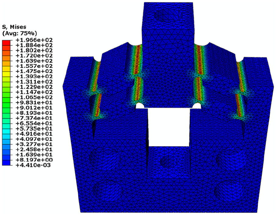
Finite element result of flexure hinge.
As shown in Figure 2, the vulnerable spots appear near the circular arc transitions which are designed circularly to promote the output performance of the flexure hinge. The maximal stress is 196.6 MPa, which is much less than the allowable stress of 65Mn (432 MPa). This result proves that the strength of the flexure hinge is enough to complete the nanoscratch tests. The stress distribution from point A to point B is extracted and shown in Figure 3(b), and the stress value is acceptable during the nanoscratch tests.
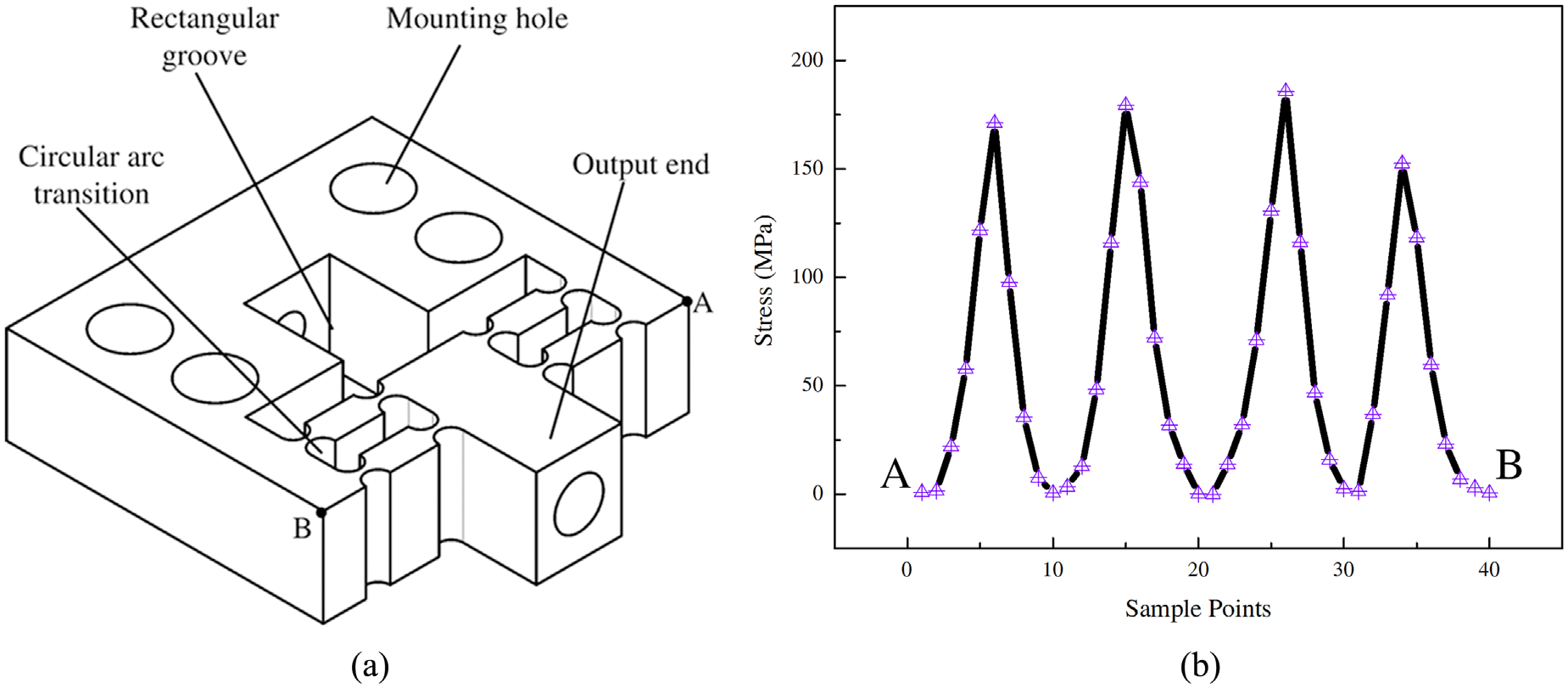
Finite element analysis of output displacement from A to B: (a) mechanical structure of flexure hinge and (b) finite element analysis result of output displacement.
Measurement module
Considering the dimensional limit, load and displacement sensors are placed at the same side of the developed device. The measurement ranges of the load and displacement sensors are 0–1 N and 0–1 mm. The two-dimension load sensor is mounted on plate B above a rotating lifting platform. This rotating lifting platform can adjust the height of the load sensor with the middle part rotating. So, different distances between two nanoscratch scars can be obtained and more experiments can be carried out with one specimen. The two-dimension load sensor works mainly using strain gages to obtain the load signal, which is amplified via load sensor amplifier finally. When the nanoscratch test is conducted, the load sensor measures the normal and friction loads at the same time.
Laser displacement sensor records the data from the beginning to the end of the nanoscratch test. Another manumotive mobile platform with 1 degree of freedom is used under the laser displacement sensor. Laser point shoots on the oblong slab and then the displacement data are acquired. The indenter is held on the two-dimension load sensor directly by the threaded connection. This kind of design reduces the displacement errors caused by the weak stiffness of middle chain between the indenter and the load sensor. Therefore, the laser displacement sensor can only obtain the displacement between the indenter and the specimen. So, the errors of measurement can be less. In addition, due to the three mobile platforms, the mounting and debugging process of the developed device can be simple and time-saving.
Control module
Closed-loop control strategy is considered more effective than the open-loop control strategy according to most scientific works. So, in this article, closed-loop control strategy is adopted to ensure the veracity and dependability of the control system. The principle and state changing diagrams of closed-loop control are shown in Figure 4. Here, take the displacement control as an example. Control parameter such as maximum output displacement is set by the software. And then the execution units work. The sensors acquire the test data, and the data are transmitted to the personal computer (PC). The data acquisition card reads and stores the data acquired by sensors. Therefore, the comparison between the set value and the actual value is realized. If the actual value is less than the set value, the execution units move forward. When the actual value is bigger than the set value, the execution units move reversely. Once the actual value equals the set value, the execution units stop. Considering the set value as a criterion, software controls the execution units. The comparing and moving processes repeat circularly until the difference value between the two values vanishes. The way of closed-loop displacement control detailed above is also applicable to the load control.

The closed-loop control diagrams of the developed device: (a) principle diagram and (b) state changing diagram.
Mechanical properties of the developed device
The simple and efficient mechanical structure of the developed device is detailed above. Mechanical property is an important criterion to assess whether the device can accomplish the nanoscratch tests well. Mechanical properties are verified as follows.
Calibration of strain two-dimension load sensor
Stress–strain curve is universally used to obtain the mechanical parameters of materials, such as Young’s modulus and elongation of materials. The main data of stress–strain curve are acquired by load and displacement sensors. For the technique of commercial displacement sensor (KEYENCE LK-G10) is well mature, the strain two-dimension load sensor is calibrated mainly here.
Before the calibration, weights are prepared to apply the calibration force. Different kinds of weight collocations provide various applied forces. Each applied force corresponds to one output voltage. The voltage value is measured by digit multimeter (Agilent 34410A). The feature points of the sensor are obtained. In addition, the linearity is important for the accuracy of sensor. Therefore, the linear curve-fitting method is adopted to get the fitting curve, equation, and linear correlation coefficient (R2) with these feature points.
Figure 5 shows the calibration results of the strain two-dimension load sensor. The fitting curve is the relationship between the load and the output voltage. The relationship between the normal load (X1) and normal axis voltage (Y1) is Y1 = 0.000151X1 − 0.00124 (R2 = 0.9998). And the relationship between the friction load (X2) and friction axis voltage (Y2) is Y2 = 0.00109X2 + 0.000453 (R2 = 0.9999). The main effective factor of the calibration equation is the value of feature point. The linear correlation coefficient (R2), which means the linear correlation degree between the two variables, is important for the sensor. If the linear correlation coefficient is more close to 1, the accuracy of sensor is better. Here, both linear correlation coefficients R2 are close to 1, which proves that the strain two-dimension load sensor has high linearity. The accuracy of the experiments will be well guaranteed later because of the reliable data.

Calibration results of strain two-dimension load sensor: (a) the result of normal axis and (b) the result of friction axis.
Output performance of the developed device
The output performance of coarse positioning module is shown in Figure 6. The displacement is measured by laser displacement sensor. The sample points in Figure 6 are the data collection points of the laser displacement sensor. With the same sampling frequency, the more the sample points are, the longer the test time is. So, the X axis means the test time in fact. Because the servo motor is utilized (not stepper motor), the curve increases continuously rather than step by step. Seen from the results, if the voltage is higher, the velocity is faster. It is worth mentioning that the curve has two cushion regions at the beginning and at the end. While the test begins, the rotating speed increases gradually from zero to the given value. It will take a little time to achieve the steady moving state. It is same as the decreasing process of rotating speed.

Output performance of coarse positioning module with different load voltages.
Additionally, the output performance of flexure hinge and piezoceramic is also considered vital to the nanoscratch tests. Figure 7 shows the actual output displacement of the precise feed module with the loading voltage increasing from 0 to 120 V. At the front of the curve, the relation between output displacement and loading voltage is approximately linear. With the loading voltage rising, the relation appears nonlinearly. This phenomenon is caused by hysteresis of the piezoceramic. With voltage applying on the piezoceramics, the polarization of each state cannot return to its original state, even after the voltage is removed. Then, the output displacement behaves nonlinearly. The maximal output displacement in this test is 14.39 µm, which is enough for nanoscratch tests.

The output displacement of the precise positioning module.
Results and discussion
In situ nanoscratch tests of single crystal copper have been carried out with the microscope. With the indenter penetrating into the specimen, the test begins when the coarse positioning module works. Like those in Figure 6, the sample points in Figure 8 are also corresponding with the test time. Because the specimen is moving, the X axis means the distance the indenter penetrates in fact. The curves of simulation and experiment are shown in Figure 8. The good meeting between the simulation and the experiment results proves that the developed device has reliable mechanical performance.
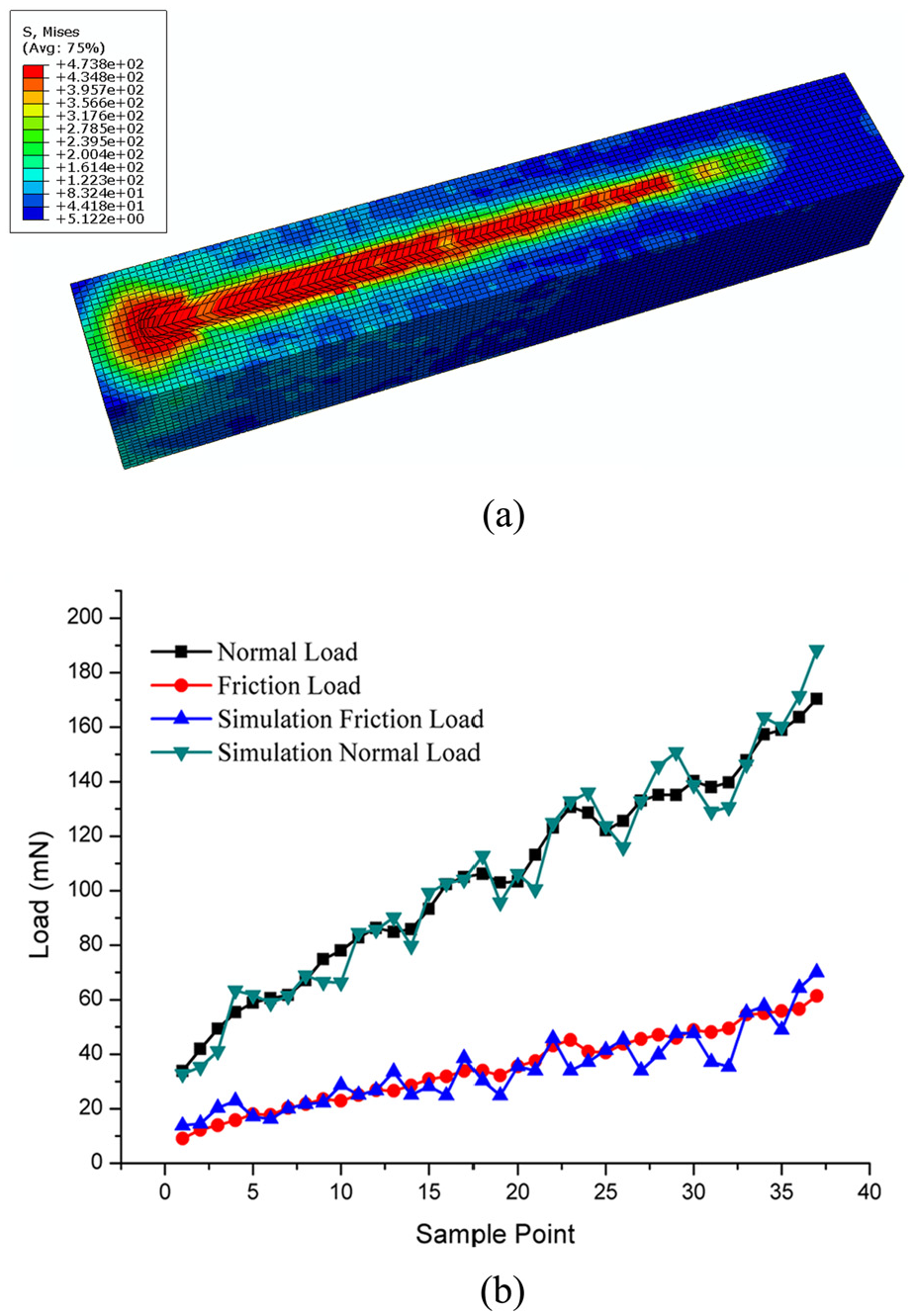
The results of nanoscratch test: (a) the result of the finite element simulation and (b) the curves of simulation and experiment.
Considering the previous works,13,14,18–20,25,26 researchers pay most attentions to the surface morphology after the scratch. They find out the wear performance of film and coating according to the residual morphology. For different materials, the results must be distinguishing. However, the varying trend is similar. In previous works,17,21 when the penetrating depth of the indenter increases, the loads increase with irregular fluctuation. In this article, the normal and friction loads are both obtained. And the varying trends are similar to the previous works. Especially, when the normal load increases, the friction load increases as well. In the rising process, both normal load and friction load fluctuate, but with different degrees. One reason for the fluctuation is that the microcracks and defects exist on the material surface. When the indenter moves across them, the load applied to the indenter varies. Another reason is that the surface material deforms from elastic stage to plastic stage with the load increasing. Failure and dislocation of materials in the plastic stage aggravate the fluctuation. So, the load acting on the indenter fluctuates. Moreover, the normal load fluctuates more violently than the friction load. The non-homogeneous structure of the material contributes to this phenomenon. The contact area of friction axis is more homogenized. So, the friction load fluctuates with a smaller range.
Figure 9 shows the real photo of the developed device and in situ continuous observation results of nanoscratch tests. The image after nanoscratch test is shown in Figure 9(b). Figure 9(c) shows the indenter under the microscope at the beginning of nanoscratch test. The situation shown in Figure 9(d) is that specimen approaches the indenter with coarse and precise positioning module working. In Figure 9(e), specimen is closer to indenter than that in Figure 9(d). Because of the reflection of incident light and observation angle, shadow of indenter appears in sight as shown. Figure 9(f) shows that the indenter penetrates into the specimen. The feasibility of the developed device for in situ nanoscratch tests is verified.
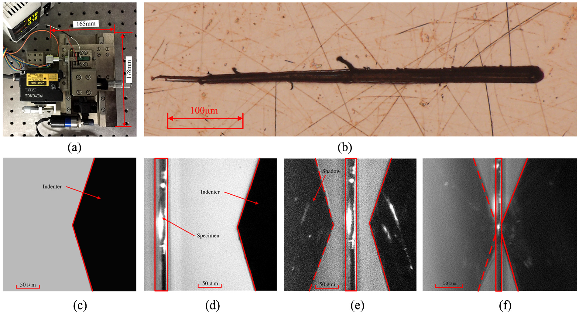
The in situ observation result of nanoscratch test: (a) real photo of the developed device, (b) the image after the scratch test, (c) beginning of the nanoscratch test, (d) indenter approaches the specimen, (e) the shadow of indenter appears, and (f) the indenter connects the test sample.
Conclusion
This article describes a novel in situ nanoscratch device with dimensions of 178 mm × 165 mm × 78 mm. This kind of device is urgently needed at present. The good teamwork of four modules ensures the in situ nanoscratch tests are completed with high accuracy. Calibration of load sensor, finite element analysis of flexure hinge, and verification of output performance are accomplished. The results of the verifying tests prove that the developed device has excellent mechanical performances. The real-time images indicate that the developed device has good compatibility with commercial microscope. The curves of nanoscratch tests with single crystal copper are obtained accurately through the comparison between finite element analysis and experimental results. The fluctuation phenomenon has been well explained. The microcracks on the material surface and the transformation of deforming stages contribute to this phenomenon.
Footnotes
Academic Editor: Xiaotun Qiu
Declaration of conflicting interests
The author(s) declared no potential conflicts of interest with respect to the research, authorship, and/or publication of this article.
Funding
The author(s) disclosed receipt of the following financial support for the research, authorship, and/or publication of this article: This research is funded by National Hi-tech Research and Development Program of China (863 Program) (Grant No. 2012AA041206), the National Natural Science Foundation of China (Grant No. 51275198), the National Natural Science Funds for Excellent Young Scholar (Grant No. 51422503), Jilin Provincial Economic Structure Strategic Adjustment Lead Special Projects (Grant No. 2014Z045), the Specialized Research Fund for the Doctoral Program of Higher Education (Grant No. 20130061110026), Program for New Century Excellent Talents in University of Ministry of Education of China (Grant No. NCET-12-0238), and Special Projects for Development of National Major Scientific Instruments and Equipments (Grant No. 2012YQ030075).