
Abstract
Lead lanthanum zirconate titanate actuators taken as one type of photo-deformable actuators have been widely applied for micro-driven systems and active vibration control of photostrictive laminated flexible structures. However, the slow response of photodeformation of single patch lead lanthanum zirconate titanate actuator greatly affects its application. In this article, the main factors for the slow response of the lead lanthanum zirconate titanate actuator are investigated using experimental method. The increasing temperature during light on state and the residual photovoltage and photodeformation during light off state are considered as dominant factors causing the slow response of the lead lanthanum zirconate titanate actuator. To gain a better driving capability of lead lanthanum zirconate titanate actuator, some effective solutions through weakening the effect of increasing temperature and eliminating residual photovoltage and photodeformation are proposed and experimentally validated in this article. Considering the effective solutions proposed in this article, a novel optical driving mechanism based on multi-patches combination is proposed.
Introduction
When the lead lanthanum zirconate titanate (PLZT) ceramic is irradiated by the ultraviolet (UV) light, the photovoltage and photodeformation are generated due to the anomalous photovoltaic effect and photostrictive effect. Therefore, PLZT ceramic shows many advantages for the micro-actuation and wireless remote control field. So, PLZT ceramic patches can be taken as the optical and wireless control actuators applied in micro-electro-mechanical system (MEMS) and micro-opto-electro-mechanical system (MOEMS).
Over the last several decades, much research on PLZT ceramics has been published. Varieties of optical micro-devices using PLZT ceramics were proposed, for example, photo-driven micro-walking machines,1,2“sunflower” device, 3 photo-driven relay, 4 electrostatic-optical motor, 5 photo-driven gripper,6,7 and photophone device. 8 Meanwhile, a large number of PLZT actuators were proposed, such as rainbow configuration actuator, 9 bimorph configuration actuator, 7 0-3 polarization PLZT actuator, 10 two-dimensional (2D) distributed opto-electro-mechanical actuator, 11 multi-degree-of-freedom (DOF) photostrictive actuator, 12 and Skew-Quad actuator. 13 Furthermore, active vibration or shape control for flexible structures laminated with PLZT actuators was carried out,14,15 for example, beams,16,17 plates,11,18,19 cylindrical shells,20–22 and spherical and parabolic shells.23,24 In addition, the constitutive models and light-induced behaviors of PLZT ceramics were researched. Luo and Tong25,26 presented finite element analysis and experimental testing for 0-3 polarized transparent PLZT plates and investigated the actuated behaviors of a 0-3 polarized PLZT-laminated plate. 27 Recently, the response characteristics of photovoltage, photocurrent, and deformation of the 0-1 polarized PLZT ceramic have been experimentally researched. 28
Whether the PLZT actuator is applied to the micro-devices or active vibration control, the photostrictive response of PLZT ceramic is the key issue for practical application. Many researchers studied the photovoltaic effect to improve photostrictive response. Poosanaas et al.29,30 investigated the influence of sample thickness and surface roughness on the performance of PLZT ceramics. Ichiki et al. 31 reported and studied a PLZT film with indium tin oxide (ITO) electrode, which photovoltaic output was highly improved and experimentally validated. Uchino et al. 32 proposed three key points (i.e. composition selection, device designing, and driving and controlling technique) were described for improving response speed of the photostriction. Luo and Tong 33 investigated the multifunctional performance of the ITO/PLZT/ITO wafer polarized along thickness direction illuminated by UV light. Nevertheless, the main reasons causing slow response of photostrictive have not yet been comprehensively analyzed and experimentally validated.
This article investigates the photodeformation, photovoltage, and temperature of single patch of PLZT ceramic irradiated by UV light. The key causes inducing the slow response of the PLZT actuator are investigated and experimentally researched. To gain the better driving capability of PLZT ceramics, some effective solutions are proven effective. Finally, a novel optical driving mechanism based on multi-patches combination for driving source is described and analyzed.
Photodeformation, photovoltage, and temperature of PLZT during light on/off states
Experimental setup and PLZT samples
PLZT ceramics show various photostrictive characteristics with different composition and processing conditions. In this article, the experimental PLZT samples are fabricated by the Shanghai Institute of Ceramics, Chinese Academy of Science. The PLZT sample heated above the Curie temperature are electrically polarized in the air. The composition ratio of La/Zr/Ti is (3/52/48). The dimensions of the PLZT samples are as follows: 15 mm (length) × 5 mm (width) × 0.8 mm (thickness). The polarization of PLZT sample with Au electrodes is along the length direction. Two identical PLZT wafers labeled as PLZT_2 and PLZT_1 will be tested in this article.
The photograph and block diagram of experimental setup are shown in Figure 1. The cantilever PLZT sample is illuminated by the UV light whose wavelength is nearby 365 nm. The photo-induced voltage between the two electrodes of PLZT wafer, the photo-induce deformation of the PLZT wafer along the length direction, and the temperature of the PLZT wafer are measured, respectively. All the experimental data are sampled, processed, and saved by the PC. The size of UV light probe is 40 mm × 40 mm. The deformation is measured by the noncontact displacement sensor (STIL Initial 12), whose resolution with averaging 10 is 500 nm. The temperature is sensed by the infrared thermometer (Optris CS series), whose temperature range is from −20°C to 350°C. The accuracy of the infrared thermometer is ±1.5°C or 1.5% of reading (whichever is greater). The photovoltage is detected by the high-impedance voltmeter (Trek 821HH), whose measuring range is from −2 to 2 kV DC. The accuracy of 821HH is better than ±1% of full scale.
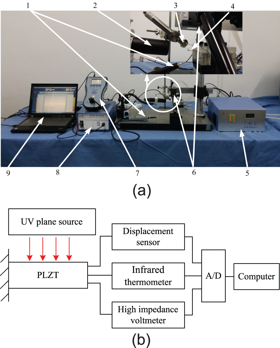
The schematic diagram of the experimental arrangement. (a) The photograph of the experimental setup: (1) sensor head of the high impedance voltmeter (Trek 821HH), (2) sensor head of noncontact displacement sensor (STIL Initial 12), (3) sensor head of the infrared thermometer (Optris CS series), (4) PLZT wafer, (5) controller of UV light source, (6) probe of UV light, (7) controller of high-impedance voltmeter (Trek 821HH), (8) controller of noncontact displacement sensor (STIL Initial 12), and (9) PC. (b) The block diagram of the experimental setup.
Experimental results and discussion
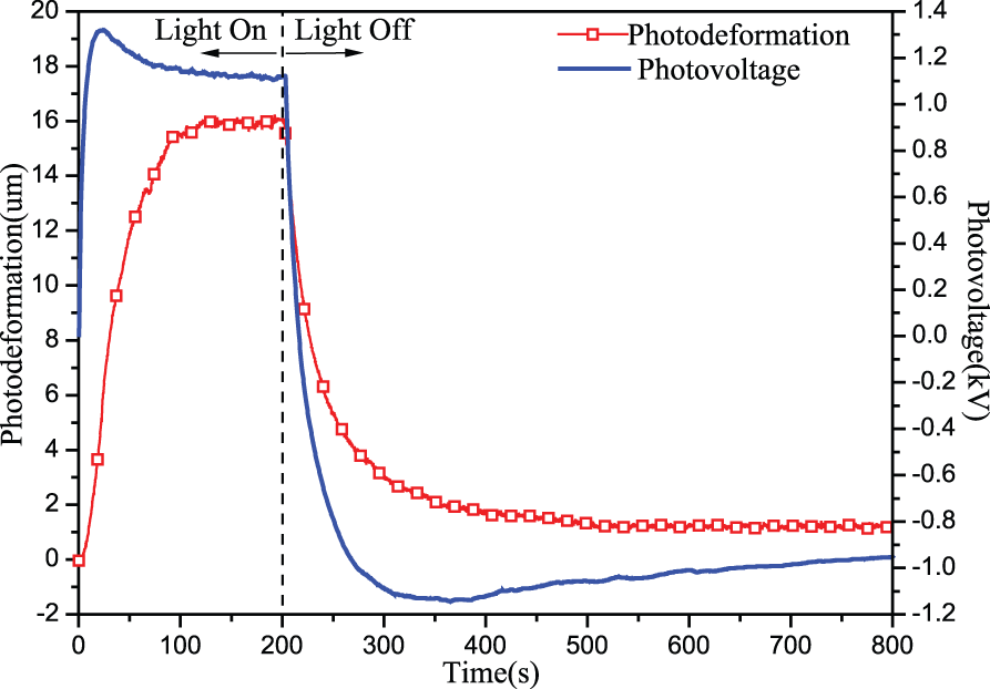
In this section, the photodeformation, photovoltage, and temperature of PLZT_1 wafer with light on/off state will be measured. The time of the light on state is 200 s, while the time of light off time is 600 s. The time history curves of photovoltage and photodeformation of the PLZT_1 wafer illuminated by the UV light of 50 and 400 mW/cm2 are presented in Figures 2 and 3, respectively. The time history curve of temperature PLZT_1 wafer is shown in Figure 4. As seen from Figure 2, when the light intensity is 50 mW/cm2, the photovoltage takes about 50 s to reach the maximum value. However, the photodeformation takes much more time (i.e. about 120 s) to reach the peak. Obviously, the response speed of photodeformation is much slower than that of photovoltage. From Figure 3, when the light intensity is 400 mW/cm2, the photovoltage only takes about 20 s to reach the peak. Meanwhile, the photodeformation takes about 100 s to reach a saturated state.

Time history curves of photovoltage and photodeformation of PLZT_1 wafer illuminated by the UV light of 50 mW/cm2.
Time history curves of photovoltage and photodeformation of PLZT_1 wafer illuminated by the UV light of 400 mW/cm2.
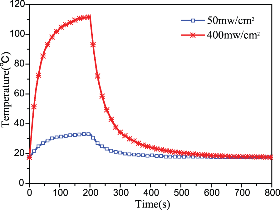
Time history curve of temperature of PLZT_1 wafer with different light intensities.
By comparing Figures 2 and 3, although the photovoltage and photodeformation become faster with the larger light intensity, the response speed of the photodeformation is still slower than that of the photovoltage. The photodeformation lagging behind the photovoltage was noticed by other researchers. 34 As seen from Figures 2 and 3, once the UV light is switched off, the residual photodeformation and photovoltage recover to the initial state gradually, which take much more time than that during light on state. The residual photovoltage and photodeformation during light off state and the photodeformation lagging behind the photovoltage during light on state may strongly affect the application of the PLZT ceramics in micro-driven and dynamic active control field.
According to Figure 4, the temperature caused by the photothermal effect gradually increases versus time during the irradiation state. The response speed of temperature is much slower than that of photovoltage. The maximum temperature becomes larger with the increasing light intensity. When the light intensity is 400 mW/cm2, the temperature varies from 17°C to 113°C during the 200 s illumination state, so the effect caused by temperature will be not be neglected in the photo-induced multi-physics fields analysis of PLZT ceramics.
Analysis of response improvement for PLZT actuation
Coupling relationships of the photo-induced multi-physics fields in PLZT ceramics
Once the PLZT ceramics have been polarized, the PLZT ceramics have piezoelectric, pyroelectric, ferroelectric, and photostrictive effect. Actually, the photostrictive effect results from the combination of anomalous photovoltaic effect, photothermal effect, pyroelectric effect, piezoelectric effect, and so on. The coupling relationship of opto-piezo-thermo-elastic fields under the irradiation of high energy light in PLZT ceramics is indicated in Figure 5.

The coupling relationships of opto-piezo-thermo-mechanical fields: 1. Anomalous photovoltaic effect, 2. photothermal effect, 3. pyroelectric effect, 4. thermal expansion effect, 5. piezoelectric effect, and 6. elasticity.
As shown in Figure 5, when the PLZT is illuminated by high energy light, the first part of electric field is generated based on the anomalous photovoltaic effect (light energy to electric energy conversion). Simultaneously, irradiated by the high energy light, the PLZT is heated based on the photothermal effect (light energy to thermal energy conversion), so the rising temperature is produced. Because of the rising temperature, the second part of electric field is generated based on pyroelectric effect (thermal energy to electric energy conversion), and one part of mechanical strain is generated based on thermal expansion effect (thermal energy to mechanical energy conversion). Meanwhile, thermal expansion strain induces the third part of electric field based on the direct piezoelectric effect. Therefore, complex opto-piezo-thermo-mechanical fields are produced when the PLZT ceramics are irradiated by high energy light.
Considering the coupling relationships shown in Figure 5 and photo-induced temperature shown in Figure 4, the slow increasing temperature causes the slow response of photodeformation. According to Figures 2 and 3, no matter how strong UV lights are applied to PLZT wafer, the apparent residual photodeformation and photovoltage still exist. The residual deformation and photovoltage prevent PLZT ceramics from application in optical micro-driven field and vibration active control. Hereby, some effective solutions to obtain better driving capability of PLZT ceramic will be researched in the next sections.
Weakening the effect of increasing temperature
Reference to the above-mentioned analysis results, the temperature of PLZT ceramic irradiated by the high energy light is confirmed as one of the main factors to induce the slow response of photodeformation. Therefore, to obtain quicker response of photodeformation, one method is weakening the effect of increasing temperature. This method will be validated by the following experiment.
As shown in Figure 6, the PLZT_1 is connected to PLZT_2 with opposite polarization directions. It means that the PLZT_1 wafer is actuated by the PLZT_2 wafer instead of directly driven by UV light. In another word, the temperature of PLZT_1 wafer remains unchanged during the PLZT_2 wafer illuminated by UV light.

PLZT_1 is actuated by PLZT_2.
In order to produce obvious deformation in the PLZT_1 wafer, the PLZT_2 wafer is illuminated by the higher light intensity of UV light (i.e. UV light of 700 mW/cm2). Time history curves of voltage and deformation produced in PLZT_1 are illustrated in Figure 7. According to Figure 7, the deformation nearly keeps in step with the voltage during the light on state. It can be obtained that reducing the temperature elevation can obviously quicken response speed of photodeformation.

Time history curves of voltage and deformation of PLZT_1 actuated by PLZT_2 with light intensity of 700 mW/cm2.
Eliminating residual photovoltage and photodeformation
In this section, the photovoltage of another PLZT sample is used for eliminating the residual photovoltage of one PLZT sample. As demonstrated in Figure 8, the PLZT_2 is electrically connected to the PLZT_1 wafer. The PLZT_1 and PLZT_2 wafers are irradiated by the two UV beams (i.e. UV_1 and UV_2), respectively. The light intensities of UV_1 and UV_2 are 300 and 700 mW/cm2, respectively. The PLZT_1 wafer is first illuminated by UV_1 for 200 s. When the UV_1 is switched off, the PLZT_2 wafer is illuminated by UV_2 for 20 s. In this case shown in Figure 8, the deformation and voltage are marked with PLZT_1_2.

Driving mechanism of PLZT_1 and PLZT_2 alternately illuminated by UV_1 and UV_2.
The photodeformation and photovoltage of PLZT_1_2 are compared with that of the single PLZT_1 illuminated by UV light of 300 mW/cm2, shown in Figure 9. According to Figure 9, it is seen that both the deformation and the photovoltage of PLZT_1_2 is little smaller than that of PLZT_1 during UV_1 on state. Nevertheless, the driving mechanism of PLZT_1 and PLZT_2 alternately illuminated by UV_1 and UV_2 still has driving ability in optical drive and control system. More than that, during UV_1 off state, the deformation of PLZT_1_2 is much faster to recover fully than that of PLZT_1 wafer directly irradiated by UV light. In a nutshell, utilizing another PLZT wafer can achieve the goal of eliminating the residual deformation.
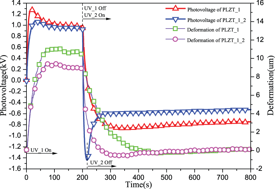
Comparison of the photodeformation and photovoltage of PLZT_1 and PLZT_1_2.
Novel optical driving mechanism with PLZT multi-patches combination
Figure 10 illustrates an optical driving mechanism based on combination of three PLZT patches. The driving source in this optical mechanism is the couple of PLZT samples (i.e. PLZT_1 and PLZT_2). The polarization directions of PLZT_1 and PLZT_2 are opposite. The driven component in this optical driving mechanism can be piezoelectric materials, such as PLZT, lead zirconate titanate (PZT), or poly(vinylidene fluoride) (PVDF) film.

Novel optical driving mechanism based on PLZT tri-patches combination.
When PLZT_1 is irradiated by UV_1 light, the positive photovoltage is applied to the driven component, which results in the positive deformation. When PLZT_2 is illuminated by UV_2 light, the negative photovoltage is applied to the driven component, which results in the negative deformation. Reference to Figure 9, the residual strain of driven component could be counteracted quickly by opposite strain, so the actuation speed of driven component is greatly improved. It is noted that UV_1 and UV_2 should be alternately turned on. Since the couple of PLZT patches for driving source is flexibly arranged, the driving mechanism shown in Figure 10 is more suitable for the distributed optical driving systems.
Conclusion
In this article, the photodeformation, photovoltage, and temperature of single patch of PLZT ceramic were experimentally investigated during UV light on/off states. The hysteresis phenomenon between the photodeformation and the photovoltage during light on state and the residual photovoltage and photodeformation during light off state were confirmed as the key factors to cause slow response of the PLZT actuator. To obtain the better driving capability of PLZT actuators, some effective solutions via reducing the increasing temperature and eliminating residual photovoltage and photodeformation were proposed and experimentally validated in this article.
Based on PLZT multi-patches combination for driving source, a novel optical driving mechanism which has better driving ability was proposed. The transmission efficiency of photovoltage applied to the driven component would be one of crucial issues in the engineering application of the novel optical driving mechanism. Improving the transmission efficiency and testing the actuation performance of the novel optical driving mechanism will be researched in next stage.
Footnotes
Academic Editor: Chow-Shing Shin
Declaration of conflicting interests
The author(s) declared no potential conflicts of interest with respect to the research, authorship, and/or publication of this article.
Funding
The author(s) disclosed receipt of the following financial support for the research, authorship, and/or publication of this article: This work was supported by the National Natural Science Foundation of China (No. 51205205), China Postdoctoral Science Foundation (No. 2012M521083), and the Fundamental Research Funds for the Central Universities (No. 30915118823).