
Abstract
Alternating current–driven electroluminescent devices on polyester fabrics were realized using a combination of coating and printing. The PEDOT:PSS front electrode was coated onto the fabric using knife coating. All other layers were digitally printed using a specially modified three-dimensional printer and three-dimensional printing software. Slicing parameters (line distance, printing speed, printing pattern) as well as other hardware parameters and ink viscosity were evaluated for each ink to obtain a good print. Final results show a complex interaction of all investigated parameters. Fully digitally printed electroluminescent devices show a luminescence of 44 lx, but combinations of digital printing and knife coating show a much higher luminescence of up to 128 lx for samples with an even smaller luminous layer thickness.
Keywords
Introduction
Textile materials are nearly omnipresent in our living environment not solely for protection and decoration but also for functional or interactive purposes resulting in “smart textiles.” Textiles are flexible, stretchable, and bendable materials, whereas conventional electronic components are rigid. Latter are composed of metals and semiconducting materials such as copper and silicon. Many technologies for the integration of electronic and “smart” functions into textile products exist. These include but are not limited to weaving, knitting, embroidering, and printing. 1 In early stages of smart textiles, electronic modules or sequins were simply embedded in a low integration depth, that is, using rigid “off-the-shelf” modules like light-emitting diodes (LEDs), sensors, integrated circuits (ICs), resistors, and capacitors. 2 These modules were embroidered on the fabric and interconnected by wires or in more advanced examples by conductive yarns.2,3 This technology is called “e-broidery®.” 4 Smart textiles were further driven by the development of conductive yarns.5,6 Some sensing functionalities could then be embedded directly into woven and knitted fabrics.7,8 Circuits and electronic components like capacitors can also be printed directly onto the fabric or other flexible substrates using silver ink as conductive material.9–13
Besides sensing capabilities, textiles with actuating functions are of great interest. Luminous textiles attract special attention in many application fields, such as exterior and interior design, lifestyle products, clothing, advertising in public space, or as eye-catchers on booths at trade fairs. Light sources like LEDs and organic light-emitting diodes (OLEDs) can be integrated on textiles using the e-broidery technology. Electroluminescent textiles offer the possibility to integrate the light source directly into the fabric. The textile touch and the appearance are not affected. In contrast to OLEDs, the fabrication of EL devices does not require special methods like vapor deposition of metals or equipment like clean rooms. Furthermore, EL devices are less susceptible to oxidation so an additional encapsulation leading to decrease of the textile haptics and character is not necessary. Although the phenomenon of electroluminescence was discovered more than 80 years ago, 14 it has attracted the attention of many researchers in the last decades again. Latest research was performed on the optimization of the production of luminous pigments,15,16 on the electrical parameters of the device 17 and on the production parameters like the composition of the different layers. 18
Suitable substrates for EL devices include but are not limited to paper, 19 PET (polyethylene terephthalate) films, glass, and textiles.20,21 Generally, two production methods must be distinguished: first, the forward architecture method with a transparent front electrode coated or printed directly onto the substrate and second the reverse architecture method, where the transparent layer is the final layer applied. 22 The forward architecture is shown in Figure 1. In case of glass or films, the substrate is preferably coated with transparent conductive oxide like fluorine doped tin oxide (FTO) in order to get a transparent conductive layer for the forward architecture method. Also, organic conductive polymers are known as electrode materials for EL devices. 23 For the luminous layer of EL devices, doped zinc sulfide pigments are used. The emitted color can be adjusted by changing the doping atoms, for example, manganese doping in ZnS results in an orange light emittance and doping with copper and chlorine results in a blue light emittance.24,25 The wavelength is shifted slightly by changing the frequency of the alternating current and more drastically by using a colored primer coating. 26 The light emittance depends on the thickness of the luminous pigment layer. Chansri et al. 27 found that the luminescence of a ZnS:Cu layer of 30 µm is higher than for thicker (50 µm) or thinner (10 µm) layers.
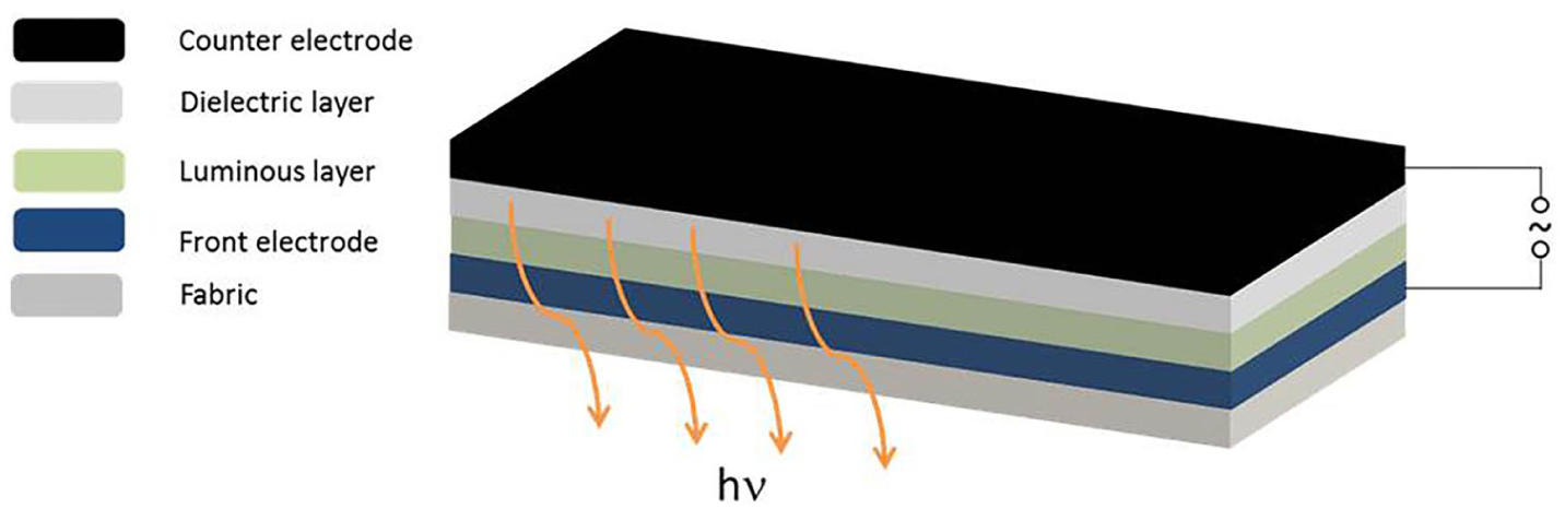
Schematic built-up of electroluminescent devices.
In literature, several production methods for EL devices were presented. A digital dispenser printing method is described for the reverse architecture of EL devices. 28 Easy realizable methods are screen printing and knife coating.23,29 Designs are transferred to screens, which then can be used many times. A great advantage of these methods is the fast and the easy transfer to a roll-to-roll application. Compared to screen printing, digital printing allows a much faster and more economic change of designs as the preparation of screens for every single design is time-consuming and expensive.
There are also reports on the production of EL devices using spin coating methods. 30 Layer thickness is controlled by the rotation speed of the substrate, the viscosity of the liquid, acceleration, and duration of rotation. Patterns are obtained by masking parts of the substrate. Compared to screen printing and knife coating, this method does not allow a roll-to-roll process. Using textile substrates, spin coating is only possible in a very limited range because fabrics take up the coating liquid due to the capillary forces between the fibers.
Above that the impact of the different application methods on the environment can be taken into account. Compared to other production methods of EL devices like screen printing, the digital printing method causes less impact on the environment. The unused ink in the cartridge can be reused and refilled into the storage container after printing. This reduces the waste of high-cost products like the luminous pigments drastically compared to screen printing, where an unneglectable amount of unused ink is left in the pores (or mesh) of the screen and the coating knife. Leftover ink in the cartridge is nearly negligible, which leads to smaller amounts and less pollution of the waste water. Also, no chemicals for the production and deletion of screens are necessary, which diminishes the impact on the environment further. The cartridges can be washed and reused; the only disposable product used in this process is the needles.
Experiment
Converting three-dimensional printer hardware to ink deposition
A versatile three-dimensional (3D) printer frame (Locxess Reptile, Villingen-Schwenningen, Germany), which can also be built as a laser cutter or computer numerical controlled (CNC) molding cutter, was assembled using Nema 17 stepper motors only for moving the x- and the y-axis. Since no movements in z-directions are necessary for the purpose of this work, a movable z-axis was not integrated. The height of the printing head is not changed during the printing process. Therefore, a manual adjustment prior to printing is sufficient and no motorized z-axis was used. The square printing area is 400 cm2. The printer was controlled by a Ramps 1.4 module connected to an Arduino Mega 2560 microcontroller. All stepper motors and the extrusion unit were controlled by a Pololu A4988 driver connected to the Ramps module. Instead of a hot end extrusion unit, a feed unit named 1000T purchased from Gonano (Breitstetten, Austria) was connected to the output of the driver stage originally intended for the use of the hot end. A syringe connected to the feed unit, which is driven by pressurized air, was mounted on the movable x-axis to extrude liquids on demand. A relay switch is responsible for enabling and disabling the pressurized air on the cartridge of the feed unit. Since the stepper motor driver circuit provides a square wave signal for operating a bipolar stepper motor on the extrusion unit, the signal had to be modified to operate the relay as depicted in Figure 2. A bridge rectifier was used to convert the AC signal to DC, while the capacitors C1 and C2 together with the internal resistance of the relay and the printer driver lead to less steep signal edges. The otherwise rectangular pulse leads to disturbances in the printer driver due to the self-inductance of the relay coil. C3 was necessary to reduce signal ripple.

Circuit for transforming the square signal from the microcontroller to a direct current used for the feed unit.
Software and settings
Since the printer is based on a 3D printer design, the printer firmware and the user interface originate also from a standard 3D printing environment. The Ramps 1.4 module is run by a Marlin Version 1.1.8 firmware, which is open source and distributed under a GNU General Public License. Some standard settings had to be adjusted for use as a two-dimensional (2D) printer, which is operated with inks and not with filaments.
In 3D printing, the firmware monitors the temperature sensor of the hot end to prevent damage if too hot or cold. It was set to read out a constant temperature of 199°C, which allows extrusion for 3D printing of most polymers. In this study, the 3D printer software Cura 3.1.1, which is available free of charge under a public license, was chosen to transform the design into a printable format. The software allows many settings, which influence the printed impression. These are in particular printing speed (up to 200 mm/s) and line distance. The latter should correspond to the needle or nozzle diameter to generate good prints. Assuming an ink which does not spread on the substrate and a needle diameter of 0.41 mm, the line distance should be adjusted to this distance. Also, the filling pattern plays a role, when the printed impression is examined. In this work zigzag, line-by-line, and concentric filling were evaluated. The height of the design is set to 0.3 mm to generate only one print layer.
Slicing was performed without any settings typical for 3D printing like building plate adhesion structures. Investigated printer parameters which influence the result are the printing speed and the line distance. Other parameters influencing the print result are air pressure for operating the feeding unit, needle size, and viscosity of the ink. The exact settings depend on the ink used and are given in the respective section.
Pretreatment of substrate
The substrate used was a white plain woven polyester fabric obtained from Schmitz-Werke, Emsdetten, Germany, with an areal weight of 200 g/m2. It was coated with polyurethane and optically brightened by the manufacturer. In a first step to assemble ACEL devices, PEDOT:PSS (Clevios S V4 from Heraeus, Leverkusen, Germany) was knife coated. The areal weight of the fabric with primer coating and conductive layer was 235 g/m2.
Inks
Functional inks were prepared on the basis of previously described coating dispersions. 23 For the luminous layer, 20.0 g ZnS:Cu, Cl particles (GG 25; Leuchtstoffwerke Breitungen, Breitungen, Germany) were dissolved in 26.6 g polyurethane dispersion Tubicoat MEA (CHT R. Beitlich, Tübingen, Germany) and 4.0 g water. The suitable needle diameter is limited by the average diameter size of 25 µm given in the technical data sheet provided by the manufacturer.
An additional dielectric ink was prepared by dissolving 5.0 g Helizarin White RTG (a dispersion of titanium dioxide particles) and 20.0 g water in 95.0 g Tubicoat MEA (CHT R. Beitlich). Lyoprint AIR (Huntsman Textile Effects, Langweid am Lech, Germany) was added during stirring in quantum satis to prevent the formation of foam.
A carbon containing counter electrode ink was prepared by mixing 50.0 g Tubicoat ELH (CHT R. Beitlich) and 10.0 g water.
Digital printing of EL devices
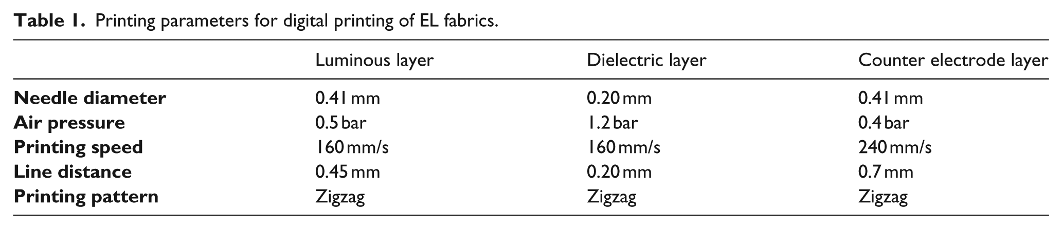
Two printing approaches were followed: (1) fully digital printing of EL devices with the printing parameters given in Table 1 and (2) a combination of digital printing and knife coating. In the latter case, the EL layer was printed and all other layers were subsequently knife coated. Shape and size of the design were the same as described for the fully digital printed EL device.
Printing parameters for digital printing of EL fabrics.
Fully digital printed EL devices
A rainbow-shaped pattern with curves and sharp edges was printed in a square shape of 30 mm as an example for the proof of concept. Between the printing of two layers, the fabric was removed from the building plate and dried for 5 min at 80°C. Marks on the printing bed allowed the refitting of the substrate. The dielectric layer was printed on top of the EL layer in a square shape of 40 mm (see Figure 3). Afterward, the square-shaped counter electrode was printed in the center of the dielectric with a side length of 35 mm. A 2-mm broad bus bar was printed in a distance of 10 mm to the dielectric. The device is shown in Figure 9.

Printing dielectric layer on luminous layer.
Combination of digital printing and knife coating of EL devices
The luminous ink was prepared and printed digitally as described above. All other dispersions were prepared according to the previously described procedure. 20 Knife coating was performed applying roll coaters. For the dielectric layer, a roll coater with a gap of 40 µm was used, and for the counter electrode, a roll coater with a gap size of 50 µm was used. The dielectric layer was coated on top of the luminous layer in a square shape of 40 mm. After drying, a 35 mm × 35 mm square was coated three times with Tubicoat ELH on top of the dielectric layer, leaving a space of 2.5 mm at the edge of the luminous layer. A 2-mm broad bus bar was coated three times in a distance of 10 mm around the luminous capacitor with Tubicoat ELH.
Measurement of EL devices
Pictures of the EL devices and the luminous emittance were recorded at 135 Veff and a frequency of 1000 Hz (Folnet 1 S from BMR GmbH, Schwabach, Germany). The EL devices were connected to the Folnet 1 S inverter via copper tape, which was adhered on the electrodes and copper wires. The luminous emittance was measured with Mavospec M600A spectrometer (Gossen Foto- und Lichtmesstechnik GmbH, Nuremberg, Germany). Bending moment and bending stiffness were measured with a bending stiffness tester TS from Frank PTI, Birkenau, Germany, in the style of DIN 53121. A sample of 60 mm length and 35 mm height was cut out and placed into the testing device. The measuring length was set to 20 mm. All results are averaged over three samples. The layer thickness was determined with a thickness gauge J-40-V from Schmidt Control Instruments and also checked with a TM 3000 tabletop scanning electron microscope (SEM) from Hitachi.
Results and discussion
Important settings for the adaption of the software to digital printing are printing speed as well as the distance between two lines. For digital printing, only the bottom layer is interesting. Three possible bottom patterns were investigated: lines, zigzag, and concentric fillings. Typical 3D printing parameters like building plate adhesion options were switched off. Also, the option “filament retraction” was switched off. This parameter is necessary for 3D printers to avoid, that molten polymer builds a blob at the extruder nozzles. In digital printing, it leads to unwanted drops of ink on the substrate, because the feed unit interprets this instruction as an order to dispense some ink.
On the hardware side, the shape and the size of the needle have an impact on the printed impression and the amount of the printed volume per time unit, respectively. Luminous ink was printed on the PEDOT:PSS-coated fabric using needles different in shape, material, and length. The use of cone-shaped polypropylene dozing nozzles led to a too fast and hence thick ink dispersion on the fabric even at the highest possible printing speed (200 mm/s) and lowest air pressure (0.1 bar). Best results were obtained with stainless steel needles, which had a length of 0.5 in.
The air pressure can be controlled with the feed unit, which also influences the print result and the dispensed amount of liquid. In Figure 3, the print is shown in action while printing the dielectric layer.
It is crucial to get a homogeneous and thin layer of luminous pigment ink. An inhomogeneous print of luminous ink leads a non-uniform light impression: parts of the design seem to be brighter or darker. If the luminous layer is too thick, no light is emitted at all because the resulting current density and electric field between the two electrodes is too low. Due to the large size and irregular shape of the luminous pigments, the needle has to be sufficiently large. The needle is blocked after printing the luminous ink for a while, when needles with a smaller size than 0.41 mm were equipped. Also, the way of filling the area is important for a homogeneous light impression. The printer settings allow three different patterns for filling the layer: lines, concentric, and zigzag. Nevertheless, the travel lines can be seen, when increasing the distance between the two lines (see Figure 8). So, the line distance has to be in the range of the needle diameter.
Printing of PEDOT:PSS
For EL devices, the front electrode must be smooth and fairly conductive. It was tried to realize also a digitally printed front electrode, but with this technique, it was not conductive. Prints become too thick, even with high printing speeds, small needles, or high line distances. Even diluting the PEDOT:PSS dispersion with water was not successful, because the resulting layer became uneven and less conductive. So, it was decided to knife coat the front electrode to produce a smooth layer. The bending stiffness after coating was 0.66 N mm2.
Influence of printing parameters on the luminous emittance
To investigate the influence of the parameters filling pattern, printing speed and line distance samples with luminous inks were printed (see Table 2) on PEDOT:PSS-coated polyester fabric. The other two layers were knife coated.
Prints with luminous pigment ink (constant values: air pressure 0.5 bar, needle diameter: 0.41 mm).

Filling pattern
Three different filling patterns were investigated: concentric, zigzag, and lines. The concentric pattern starts in the middle and fills the design in a helical path; zigzag means that the printer head moves in zigzag way over the substrate dispensing the ink continuously; and the line pattern is related to the zigzag pattern, but ink is dispensed only unidirectional. The other parameters were kept at values comparable to the investigations on printing speed and line distance. So, the printing speed was set to 160 mm/s, line distance to 0.45 mm, and the air pressure to 0.5 bar for the luminous layer. The resulting EL devices are shown in Figure 4. All three patterns show good and bright electroluminescence with a luminous emittance between 44 and 48 lx. However, the concentric pattern has the disadvantage that the transition between two shapes is in the middle of the patterns, whereas the transition of the two others is at the edge and the line-by-line filling pattern takes nearly double time to be printed, because after each line a transition move is necessary. During that movement, no ink is dispensed.

Filling pattern of EL layer: (a) zigzag (P1), (b) concentric (P2), and (c) lines (P3).
Printing speed
With a needle diameter of 0.41 mm, three different printing speeds were investigated: 80, 120, and 160 mm/s. All other parameters were kept constant. The air pressure was set to 0.5 bar, the line distance to 0.45 mm, and the pattern was filled using zigzag lines. In order to study the influence of the printed EL ink, the following devices were assembled with coated dielectric layer and coated counter electrodes. The three described EL devices are shown in Figure 5.

Three printing speeds: (a) 80 mm/s (S1), (b) 120 mm/s (S2), and (c) 160 mm/s (S3).
The luminous emittance increases with the printing speed; although not visible in the photographs due to exposure limitations, it could clearly be measured. The correlation between luminous emittance and printing speed is shown in Figure 6. At first glance this seems not to be comprehensible, because less luminous pigments printed per area would lead to a lower emittance. But it can be considered that the thickness of the luminous layer decreases with higher speed and therefore the electric field increases leading to an elevated level of luminous emittance. However, the relation between luminous intensity and electric field strength seems to be rather complex and dependent on the type of the applied EL particle. Furthermore, the local electric field around the particles is altered by the particle distribution in the polymer matrix and the morphology of the covering dielectric coating layer. Therefore, the given experiments do not provide sufficient data to analyze this complex situation. Besides that, the data show indications that thinner layers of the PU matrix with the luminous particles will give higher intensities. Given the hypothesis that there are two opposing effects influencing the light intensity, on the one hand, the electric field depending on the distance between the electrodes and, on the other hand, the concentration of luminous particles due to different layer thickness, it can be concluded that the factor dominating the light intensity of the construction is the field strength. Since some authors report increasing numbers of local emission centers on such particles by increasing voltages, it can be assumed that a saturation of the particles in these experiments was not yet reached. 31
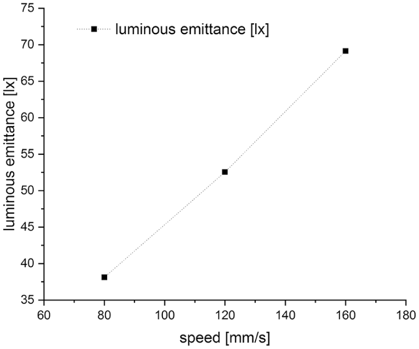
Correlation between printing speed and luminous emittance.
Line distance
Also, the chosen line distance influences the luminous emittance. Here, it was shown again that the concentration of luminous pigments per area has an impact on the luminous emittance (Figure 7), mainly due to the same reasons as previously described. The sample L5 (Figure 8(e)) with a line distance double the needle size is the brightest sample. But in this sample, some areas are not covered with EL ink and the printing path can be seen. Smaller line distances lead not only to less luminous emittance but also to better light impressions. When the luminous pigment layer becomes too thick (Figure 8(a) and (b)), the edges of the design can be distinguished from the center part of it. The latter areas emit less light than the rest of the device, which leads to lower total luminous emittance. In particular, this can be seen comparing Figure 8(a) and (e).

Rainbow pattern printed with EL ink at a speed of 160 mm/s and zigzag filling pattern, line distance: (a) 0.30 mm, (b) 0.41 mm, (c) 0.45 mm, (d) 0.50 mm, and (e) 0.82 mm.

Correlation between line distance and luminous emittance.
Fully printed EL devices
Printing parameters for a fully printed EL device are given in Table 1 and the light impression in Figure 9. Although the multilayer structure becomes quite rigid, it is still bendable (Figure 9).

Fully digitally printed bendable EL device.
The luminous emittance of this device is 44 lx. The decreased luminous emittance of this device compared to the previously described devices is due to the thickness of the dielectric layer. In the samples above, the dielectric was coated on top of the luminous layer and therefore it was thin. However, with this method, the layer thickness cannot be adjusted exactly, because it is attributed to many parameters. The digitally printed EL device has a bending moment of 1.19 N mm2. A coated EL device has a bending moment of 0.66 N mm2. The same must also be taken into account for the bending stiffness. The layer stack is thicker, if digitally printed.
Layer analysis
The digitally printed EL devices were investigated by SEM micrographs. In a cross section of an EL device (Figure 10), the luminous pigment layer and the counter electrode layer are well distinguishable due to their thickness. Between these two layers, the titanium dioxide containing dielectric layer is visible. This fact is illustrated by the SEM/EDX micrograph, which is shown in Figure 11. The zinc sulfide pigments are colored in purple embedded in the polymer matrix, and the dielectric layer, which contains titanium dioxide, is depicted in orange.

SEM micrograph of digitally printed EL device (cross cut).
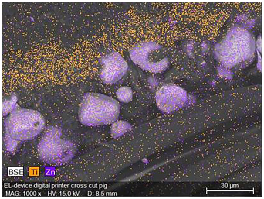
SEM/EDX micrograph of digitally printed EL device (cross cut). Titanium is colored in orange, zinc in purple, layer assignment the same as in Figure 10.
The flow rate is controlled by the air pressure and therefore constant. Hence, the layer thickness decreases with the increasing printing speed. For the slowest printing speed, that is, 80 mm/s, a thickness of 120 µm was measured. The highest printing speed results in a layer thickness of 50 µm, and with a speed of 120 mm/s, the layer thickness was found to be around 100 µm. These values were also verified by an SEM analysis and correlated with the increased luminous emittance for thinner layers. Also, a larger line distance leads to thinner layers, because the ink spreads on the fabric, that is, the line width becomes larger than the nozzle size.
Due to the facts, that the layer is very thin and the substrate itself is uneven, the PEDOT:PSS layer cannot be resolved in the SEM cross-cut micrographs. With the settings given in Table 1, a layer thickness of approximately 50 µm was realized for the luminous layer. The thickness of the dielectric layer was determined to be between 20 and 35 µm, whereas the counter electrode layer is in the range from 90 to 110 µm.
Conclusion
The presented dispenser printing method allows a fast and low-cost production of EL devices with a high luminescence. The design can be prepared easily using simple 3D printing software, which was the most time-consuming part in this work. Compared to the traditional screen printing, the required time for screen preparation is not applicable. The shape and design of the luminous area can be chosen freely. Also, complicated designs can be printed easily. Screen printing or knife coating of the PEDOT:PSS front electrode is obligatory. Prints of the front electrodes with the dispensing method are too thick, which has a negative impact on the transparency. Diluting the PEDOT:PSS dispersion with water had an negative effect on the conductivity. The luminous layer, which is responsible for the design, is printed with the presented digital printing method. Both other layers, dielectric and back electrode layer, can either be printed digitally or be knife coated. Compared to screen printing, the impact on the environment is reduced.
Footnotes
Declaration of conflicting interests
The author(s) declared no potential conflicts of interest with respect to the research, authorship, and/or publication of this article.
Funding
The author(s) disclosed receipt of the following financial support for the research, authorship, and/or publication of this article: This research was funded by the ZIM program of the German Federal Ministry of Economic Affairs and Energy under the support code ZF 4102202CJ6.