
Abstract
The photovoltaic industry is a strategic and sunrise industry with international competitive advantages. Driven by policy guidance and market demand, the new energy industry represented by the photovoltaic industry has been a significant emerging industry in developing the national economy and people’s livelihood. Stable photovoltaic power generation capacity supply is a critical issue in the photovoltaic industry. With the popularization of industrial Internet technology and Internet of things technology, more and more academic and industrial circles begin to introduce new technologies to provide the latest research results and solutions for the photovoltaic industry. Electroluminescence is a standard detection method for photovoltaic production in the application of solar energy production. This method uses human vision to detect whether the solar silicon unit is defective. In this article, due to the three core pain points in traditional electroluminescence detection: low efficiency of offline identification, low accuracy and accuracy of data detection, and no online diagnosis and prediction, we carry out ISEE research based on edge computing unit. ISEE uses the edge device to collect the real-time video image of the solar panel through the camera. Then it uses the powerful neural network processing unit module of the edge computing unit, combined with the convolutional neural network algorithm transplanted to the edge, to detect the defects of solar panels in real time. It completes the research on intelligent detection of photovoltaic power generation production defects based on the Internet of Things. After a large number of experimental design verification, ISEE effectively improves the automation degree and identification accuracy in the production and detection process of solar photovoltaic cells and reduces the cost of operation and maintenance. The accuracy rate reaches 93.75%, which has significant theoretical research significance and practical application value.
Introduction
By a new round of energy revolution, photovoltaic power generation has become the leading choice of new energy development
1
for human beings in the future. California, which has the largest economy and enormous energy consumption in the United States, has achieved the goal of more than 3% of renewable energy generation in early 2017. China has announced that it will strive to reach the peak of carbon dioxide emissions by
The standard solar panel modules without obvious defects are shown in Figures 1 and 2. Their colors are the same; however, there are many kinds of solar panel modules with defects in the production process.4–6 Black spot: there are irregular black blocks, and the color is darker than other blocks; black center: the center of the battery is round black. In some severe cases, it is black and is ring shaped. (It is likely found in single-crystal cells at present in Figure 3); grid break: black linear traces with different lengths along the gridline direction on the cell’s surface; cracks: severe or even broken cells caused by extrusion and collision due to various production forces. 7

Normal silicon wafer.

Normal silicon wafers images.

Defective silicon wafer.
At present, solar panel defect detection mainly relies on manual detection, which has low efficiency, high labor cost, and low accuracy. Therefore, it is essential to detect the defects of solar panels automatically, accurately, and efficiently in actual production. Huang Yuwen and others put forward the defect detection method of solar panels by unmanned aerial vehicle (UAV) aerial photo splicing. In their scheme, first, the collected images are preprocessed and corrected, and then the images are stitched to extract the image features of defects in the production of solar panels. Different defects can be distinguished and detected by analyzing the characteristics of defects such as cracks, missing corners, broken poles, broken grids, and stains regarding the area, length and width, rectangularity, and direction after production. However, there is not enough guidance for defect detection in the production process. Therefore, this article focuses on the following three aspects of research work:
The online detection process of solar panels in the production process was optimized.
In order to improve the intelligence of detection, ISEE, a neural network algorithm based on edge computing units, is studied.
Through a lot of parameter adjustment and algorithm optimization, we improved intelligent detection accuracy.
In order to better analyze and summarize our work, the structure of this article is as follows: in the first section, we introduce the object and background information of this article. In the second part, we analyze the latest research results in the current academic field. The following section introduces the core algorithm, system architecture, detection process, and algorithm design. The fourth part verifies the system’s effectiveness through experimental design and data processing and analysis. In the fifth section, we summarize this article.
Related work
Solar cell detection technologies have also been widely studied.8,9 Cheng Hua et al. proposed a defect detection method for solar cells based on signal mutation point correction. Based on the one-dimensional discrete signal, the method detects the sudden change points in the image column by column in the wavelet domain to capture the signal mutation point and uses the energy barycenter method to correct the background of the defect image. Finally, a simple algebraic fusion of the original and restored background images highlights the defect area. Xiaoliang Qian et al. carried out an in-depth inspection on the microcracks of solar cells. An adaptive deep feature extraction scheme without any supervision training is proposed based on the adaptive depth feature. Finally, they introduced visual saliency into micro-crack detection. 10 Kim et al. 11 carried out the relevant solar panel defect detection experiments in the outdoor environment and obtained the optimal scheme of solar panel detection in the experiment. In terms of real-time sensing technology and visual perception, Xiang et al. 12 used tactile devices to accurately sense people and obtain outdoor remote switching server (RSS) maps. Takashi Fuyuki et al. made an in-depth study on the source of defects in solar panels. He believed that the photographic measurement of electroluminescence (EL) under forwarding bias voltage is a powerful diagnostic tool for studying the material characteristics and process defects of silicon (Si) solar cells. Under the condition of forwarding bias, the solar cell emits infrared light (wavelength about 1000–1200 nm), and its intensity reflects the number of minority carriers in the substrate layer. Therefore, we can detect all the factors affecting the carrier density, such as minority carrier diffusion length (or, in other words, lifetime) and recombination velocity at the surface and interface. They can capture the intensity distribution of EL gray images in 1 s with a CCD camera. The detection area only depends on the optical lens system at the range of 1–1.5 m.
This fast and accurate method is superior to conventional scanning methods, such as laser beam–induced current (LBIC). They believe that they can classify the defect types of crystalline silicon solar cells by measuring the temperature on the cells. However, this manual method does not use automatic and intelligent ways to optimize the defect detection method further. Sergiu Deitsch has studied two methods for detecting such defects in a single image of photovoltaic cells. The hardware requirements of these methods are different, depending on their respective application scenarios. Another efficient method centers on hand-made features classified in support vector machine (SVM). In order to obtain strong performance, the authors have studied and compared various processing variants. The more hardware demanding method uses an end-to-end deep convolution neural network (CNN), which runs on the graphics processing unit (GPU). Both methods trained 1968 cell images extracted from high-resolution EL intensity images of single-crystal and polycrystalline photovoltaic modules. CNN is accurate, with an average accuracy of 82.44%. Although the author has studied two processing variants in this process, he fails to study their differences. Simultaneously, the offline detection method based on GPU still has poor real-time performance and limited computing power. Alexander barter et al. introduced a classification pipeline based on deep learning to operate EL images. These approaches include image preprocessing for distortion correction, segmentation, and perspective correction, and deep CNNs for solar defect classification, emphasizing processing highly unbalanced data sets. The influence of a few oversampling and data amplification on the system accuracy is studied. The author verified the performance of the proposed classification on the actual pipeline. However, in the output of discrete classification, the continuous absolute number index is not given, so the accuracy detection factors are further analyzed. These studies have proposed solutions from various aspects for this problem, but the accuracy of online detection of solar cells is not high. The degree of automation is also low. Moreover, few authors propose integrated applications at the architecture level. Therefore, there is an urgent need for a more efficient, accurate, and simple detection method to realize solar panels’ intelligent detection. Therefore, this study used edge equipment to detect the defects of solar panels and formed a complete framework to solve the system theory. The edge device collects the solar panel video image through the camera in real time and then uses its own powerful NPU module, combined with the CNN algorithm transplanted to the edge, to detect the defects of solar panels in real time, which provides a new solution for the online monitoring of solar panels.
ISEE overall system design
We collect a large amount of operation state data in the photovoltaic power station’s daily operation. The operation of a photovoltaic power station needs to follow the operation law of the equipment from the massive data, accurately predict the power generation of the equipment, and early warn the possible faults. Mehta et al. 13 proposes a method for analyzing the pollution and defects of solar panels based on a CNN. Our study introduces the cloud operation and maintenance system of solar photovoltaic power generation based on big data. We study the main problems by designing intelligent recognition systems of solar panels based on edge devices.
Architecture design
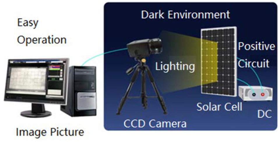
With the rapid development of artificial intelligence (AI) chips, edge computing has gradually become an important research hotspot. Xiang et al. 14 combine low-rank theory with edge computing and finally achieve the function of large-scale traffic data recovery through experiments. In this study, embedded devices are used in the edge to detect the defects of solar panels in real time, which effectively improves the degree of automation, recognition accuracy, and dramatically reduces the cost. The overall block diagram of defect detection of solar panels is shown in Figure 4. In the whole system, the PN junction of the solar panel is positively electrified by a DC power supply, which makes the solar panel produce positive bias voltage and emit infrared light. When the electrons are injected into the solar cell and recombined with the existing holes, the energy will release in the form of photons in the local range. The wavelength of the released photons is similar to the infrared wavelength, and then the image of the solar panel is collected in real time by the industrial infrared camera placed in the darkroom.

Structure defect detection system of solar cell.
Compared with the traditional offline detection, this article also proposes a new architecture based on online detection as follows: as can be seen from Figures 5 and 6, this study adopts the design idea of online system architecture based on a BS architecture.
Traditional system architecture.

Solar eye system architecture.
B/S structure is browser and server structure. In this structure, we set the user interface in the browser and set the main transaction logic on the server-side, forming the so-called three-tier structure. This architecture dramatically simplifies the client computer load, reduces system maintenance, upgrades cost and workload, and reduces users’ total cost (TCO). For this system’s design, the end-user only needs a computer that can access the Internet. With the rapid development of the industrial Internet, mobile and distributed design are becoming more popular, requiring our system to have scalability. On one hand, this method can enable us to access remotely; simultaneously, it can also satisfy the system to process distributed data. Simultaneously, this architecture can allow super managers to upgrade the system software uniformly in a large-scale application, significantly saving maintenance and upgrade costs.
Workflow of system
In this system, the USB camera sends the collected image to the edge device through the USB port, and the edge device first uses OpenCV (open source computer vision (CV)). The image processing module in the library is to preprocess the received image and then the preprocessed image is taken as the input of the neural network model, and the output result is obtained through neural network reasoning to detect whether the current solar panel has defects. The detection flow of the system is shown in Figure 7.
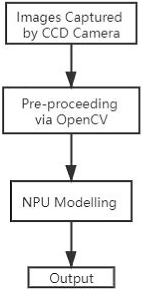
Workflow.
ISEE algorithm
In this study, we use CV and CNNs to solve the defect problem of solar panels and edge devices to detect the defects in real time.
Design of edge computing unit
In the background of intelligent manufacturing, the proliferation of terminal network equipment brings new challenges to data operation and maintenance, scalability, and reliability. Edge computing addresses these challenges by creating an open platform that integrates core functions like network, computing, storage, and applications. The development of edge computing enables computing to move from the centralized data center to the network’s periphery. It also enables intelligent services close to manufacturing cells to meet critical requirements, such as agile connectivity, data analysis through edge nodes, highly responsive cloud services, and privacy policies. Edge computing can use the embedded computing power of field devices to realize device autonomy based on distributed information processing. Also, edge computing supports the demand of digital manufacturing enterprises to configure intelligent factories quickly. Intelligent factories must adapt to the personalized needs of users and the dynamic changes of production conditions.
The research progress based on edge computing is also developing rapidly. Due to the limitation of a cloud platform, Lopez and others think that edge computing is necessary to move data and services from centralized nodes to the network edge. Condry et al. introduced a model using intelligent edge Internet of things (IoT) devices for safe and fast response of industrial IoT control operation. With the application of the IoT in the industrial field, Georgopoulos and others proposed a manufacturing roadmap of the IoT combined with cloud edge computing. Because edge computing run on the IoT devices’ peripherals, it can support these mobility and geographic independence requirements.
The physical proximity between computing and mobile devices makes it easier to implement low-end delay, high bandwidth, and low jitter services at the network’s edge. The scope of edge computing extends the range of IoT embedded devices with limited storage, cache, and processing capabilities to the edge near the terminal infrastructure. This study found that the edge computing unit has a powerful NPU neural unit for AI hardware acceleration. Under the same circumstances, the NPU’s AI computing power consumption is less than 1% of the GPU, significantly saving the hardware cost in a large amount of data processing in the solar photovoltaic industry.
Edge computing framework based on CNN
We run the convolutional neural networks (CNNs) in real time on edge computing unit to detect solar panels’ defects to transplant quickly. A CNN is a successful algorithm in AI and a powerful candidate for many CV algorithms. 15 However, the computational complexity of CNN is much higher than that of traditional algorithms. Usually, with the help of GPU acceleration, CNN-based applications are widely deployed on servers. However, the solution based on CNN is still too complex to be applied. To speed up CNN’s development, people have designed the whole design process, deployed quickly, and run efficiently on edge computing units. The system memory requirements, computational complexity, and flexibility for CNN mapping on embedded edge computing units are summarized. Based on these requirements, this article proposes a programmable and flexible CNN edge computing framework. As a feature extraction step, 5 CNN has excellent performance, but it is not easy to achieve in daily industrial applications and equipment due to its high computational complexity. For the inference of a 224 × 224 image, a large CNN model can involve 40 g operations (multiplication or addition). 2 In practical application, the more considerable image cost is much more than this order of magnitude. Therefore, we usually deploy CNN-based applications on cloud servers. For the industrial application equipment, especially in the solar panel monitoring unit, the traditional CPU platform is challenging to process the CNN model with acceptable processing speed. It is even worse for the target detection tasks that need real-time processing. The high utilization rate of GPU depends on the number of images suitable for parallel processing. However, for the real-time detection of industrial solar cells, mass production is not practical.
This article extends the whole process to a complete design process and maps CNN to the embedded edge computing unit. The process consists of three parts: the strategy of compressing the original network into fixed-point data quantization. Parameterized and run-time configurable hardware architecture supporting various networks and platforms. In this article, we design a compiler to map the CNN model to the hardware architecture. Experiments on edge computing units show that the proposed design process can achieve CNN acceleration with high energy efficiency.
CNN research includes a series of aspects. As the name suggests, the most important layer in CNN is the convolution layer. The full connection layer, nonlinear layer, and convergence layer (downsampling layer) are important parts of the neural network. The convolution layer uses the trained filter to perform two-dimensional convolution on the input feature mapping to extract local features. In order to extract high-level features, it is usually necessary to cascade multiple transformation layers. In the final stage of CNN, it is usually used as a classifier. The correction linear element (ReLU) is one of the most commonly used functions. Hyperbolic tangent function and sigmoid function are often loaded into various neural networks used in the downsampling collection layer. 16
In this article, as the research model comprises multiple convolution layers and top fully connected layers and contains correlation weight and pooling layer, a CNN is used to intersect other depth networks. 17
In Figure 8, from left to right, the first image is the original image, and then the image is rotated left and right, up and down, 90° rotation, 180° rotation, 270° rotation, random brightness, and random contrast adjustment and adjustment. Through these technologies, data enhancement is realized to expand the number of samples.

Actions on images.
When the data set is expanded, all images’ size is cut to 100 × 100, and these images are normalized to facilitate the learning of the neural network.
Algorithm model design process
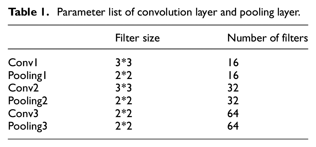
This article combines CV and CNN technology to detect the defects of solar panels, which uses three layers of convolution layer and three layers of pool layer, two full connection layers and one output layer. The network architecture is shown in Figure 9.

Algorithm model design process.
Convolution layer: the purpose of this layer is to extract the features of the input image. Each node is just a small piece of the upper neural network. It moves a filter from the upper left corner of the neural network to the lower right corner and calculates each corresponding identity matrix in the movement. The filter size of the convolution layer is 3 * 3. Activation function: a nonlinear activation function is added after each convolution layer. The purpose of adding a nonlinear activation function is to make the neural network more expressive. Because the linear function is used, the model cannot work accurately in many cases. The nonlinear activation function mainly includes the sigmoid function, tanh function, and relu function. This article uses the relu activation function, which can speed up the training speed compared with the previous two functions

Pooling layer: this layer reduces each feature graph’s dimensions while retaining important information in the feature graph. The commonly used pooling methods are average pooling and maximum pooling, and the maximum pooling is used in this article. The filter size of the pooling layer is 2 * 2.
Model neural network structure of the convolution layer and pooling layer parameters of the network are shown in Table 1.
Parameter list of convolution layer and pooling layer.
The main purpose of this article is to extract the full layer connection feature. This article shows
Dropout: To prevent the model from the over-fitting phenomenon, dropout technology is adopted, which mainly can discard some neurons randomly during training. In this article, keep prob = 0.5 is set.
Batch normalization: in this article, the input image has been normalized in image preprocessing, but the input data distribution in each neural network layer changes during training. This is because updating the front layer’s training parameters will lead to the change of the input data distribution in the later layer, leading to the change of the input data distribution in each layer. Moreover, if there is a slight change in the network’s front layer, the latter will gradually accumulate and enlarge the change. Therefore, this article uses a batch normalization algorithm to solve the network layer’s problem, making each layer’s neural network input keep the same distribution, accelerate the model’s training speed, and improve its performance.
Normalization is used before relu, and the specific implementation process is as follows


where
In this article, the size of a single batch is set to 64. First, formula (1) obtains the average value of the current batch, then formula (2) calculates the variance of the current batch, and then uses a formula (3) to get the normalization processing of input data. Finally, the data after batch normalization is obtained by formula (4), which is used as the next layer network input.
L2 regularization: in addition to using dropout technology to prevent over-fitting, this article also adds L2 regularization to the neural network, which can be regarded as a penalty term for the loss function. Assuming that the loss function of the model is, which represents all the parameters of the neural network, after adding L2 regularization, the loss function becomes

In the process of model optimization, it is necessary to optimize the new loss function
In this article, adding L2 regularization to the model can limit the weight’s size very well. Making the parameters as close to 0 as possible can prevent the random noise in the model’s training data from fitting arbitrarily to avoid the model’s over-fitting. The coefficient set in this paper is 0.0001.
Experimental evaluation and verification
Experimental preparation
The experimental conditions are as follows (Figure 10, Table 2):

Hardware platform.
System hardware configuration list.

The main control chip of the ISEE edge computing unit is the rk3399 pro version. Its CPU is an arm 64-bit processor (dual-core cortex-a72 + quad-core cortex-a53), and the central frequency is up to 1.8 GHz. NPU neural unit is also built into the chip to support AI hardware acceleration. Under the same condition, the power consumption of NPU for AI operation is less than 1% of GPU. The gateway has a multi-channel USB interface. We connected the camera to the gateway through a USB interface, and a 12 V power supply powers it. The system has been running for over years in Perimar Group, Italy, as shown in Figures 11 and 12.
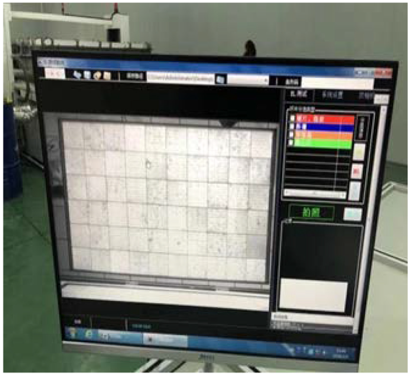
System operation test chart.

System operation test in factory.
Data proceeding
This article collects 300 images of EL, then calls the image processing module in OpenCV (Open Source CV Library) library. By making use of rotating images, adjusting the picture contrast map and luminance method to make 100 single expanded images, we get the final data set is 30,000, and 24,000 of them act as training sets and 6000 as validation sets. We generated 30,000 JPEG format images in the above section. If we use the method of directly reading the pictures stored in the disk during the actual training, we need enough GPU memory to store the training data. Purchasing GPU with more significant memory means a higher cost. To solve this problem, TensorFlow uses the tfrecord format to store data uniformly, storing image data, label information, image path, and different types of information of width and height together for unified storage, to manage different attributes conveniently and effectively. In this article, to improve the reading efficiency, the training set and verification sets contain two separate folders, and then a tfrecord format file of the training set and tfrecord format file of the verification set is generated, respectively.
Evaluation and verification
In this article, we set the learning rate of the model as 0.0001. After 68 epochs of iterative learning, the model’s accuracy rate in the training set is 96.875%, and the verification set’s accuracy rate is 93.75%. (the red curve represents the accuracy curve of the training set, and the blue curve represents the accuracy curve of the verification set (Figure 13)). The model’s deviation in the training and verification sets is slight, which shows that the model’s generalization ability is strong.

Accuracy curve of the model training set and verification set.
Conclusion
In solar photovoltaic power generation, the panel’s safety is related to the safety and efficiency of the whole system. It has always been a concern for industry and academia to detect whether there are defects. In industry, people pass 1-40 mA forward current to the cell through EL to act on both sides of the diffusion junction. The forward bias voltage excites the atoms in the ground state, making them in the excited state. The atoms in the excited state are unstable and emit spontaneously. EL depends on many non-eq7 carriers injected from the diffusion region to emit photons, and then these photos are captured by a CCD camera. By the relationship between minority carrier lifetime, density, and light intensity, we can detect the silicon wafer defects from the exposure degree of negative film in a darkroom. In this process, there are many difficulties. In this article, we proposed a fast, stable, and predictable algorithm to effectively find the defects in solar modules to find the production problems and eliminate them in time to improve the process. In the future, we will focus more on algorithms for dealing with high-speed proceeding mass amount of image data at the same time and how to save proceeding and storage in this process. Through these studies, we can finally improve efficiency and stabilize production in the whole photovoltaic industry.
Footnotes
Handling Editor: Yanjiao Chen
Declaration of conflicting interests
The author(s) declared no potential conflicts of interest with respect to the research, authorship, and/or publication of this article.
Funding
The author(s) disclosed receipt of the following financial support for the research, authorship, and/or publication of this article: The paper is supported by the National Major Scientific Research Instrument Development Project (grant no. 6202780085); National Key