
Abstract
Presently, it is difficult to measure the characteristic impedance of embroidered microstrip line for its conductive anisotropy directly. The published work had proposed to use S-parameters to estimate the port impedance of a balanced dipole antenna, and it cannot be used to calculate the characteristic impedance of microstrip lines with one arm. Thus, it is still a problem on measuring and obtaining 50 Ω characteristic impedance of embroidered microstrip line. Therefore, taking the reflection coefficient as an intermediate variable, this work proposes to use return loss
Introduction
As an important part of the electronic radio frequency device, such as microstrip antennas,1,2 resonant antennas, 3 microstrip line is the carrier and the transmission tool of energy and information. In order to obtain the maximum energy transmission, the microstrip line needs to achieve impedance matching with both ends of the connected device, 4 and its characteristic impedance is usually 50 Ω. Compared with the microstrip line on the traditional PCB board, wearable microstrip lines are typically made from flexible conductors. 5 Like all wearable microstrip lines, they should be light weight, low cost, flexible and seamlessly integrated with clothing. 6 Thus, embroidery technique with conductive threads is a compelling approach for the fabrication of such microstrip lines.
For the embroidery microstrip line, its conductor strip is formed by embroidering the conductive yarns into the fabric, which is different from traditional conductor strip deposited on the substrate. Thus, it is hard to determine substrate of embroidered microstrip line and design its characteristic impedance accurately, and further affecting the signal transmission due to the impedance mismatch. Therefore, it is very important to investigate the impedance of embroidered microstrip line for better application in flexible electronic.
At present, the common instruments for measuring the impedance of microstrip line directly include: time domain reflectometer (TDR) and impedance analyzer. Locher
7
et al. used time domain reflectometer to test the impedance of a transmission line printed with ink. The TDR method can calculate the position of the impedance change point in the transmission path by measuring the time value from the reflection point to the signal output point, and it can be used for fault analysis in circuits. On the other hand, the signal has more high-energy and rich frequency information in frequency domain reflection technology, and can identify reflected waves.
8
The change of characteristic impedance in frequency domain is usually considered to analyze the transmission, reflection and loss of signals. Machappa
9
et al. used Hioki impedance analyzer to test the impedance spectroscopy of screen-printed UHF RFID tags conducting polyaniline (PANI)/zinc tungstate (ZnWO4) composites in the frequency range of 50 Hz to 5 MHz. The above-mentioned TDR and impedance analyzers obtain various electrical parameters of samples by using probes to contact the sample. Unlike the conductors printed with conductive ink and the label printed by the screen, the conductor of embroidered microstrip line is uneven and discontinuous. Then, the characteristic impedance of embroidered microstrip line would change with the change of contact position and direction of the probe and the samples, and the methods of TDR and impedance analyzers are not applicable to embroidered microstrip lines. In addition, Qing
10
et al. presented S-parameter method (
In view of the difficulty in measuring the impedance of embroidered microstrip line, this work proposed a method for calculating its impedance in the frequency domain. First, the return loss (
Calculation method on characteristic impedance of microstrip line
In order to obtain impedance of a balanced dipole antenna, Qing
10
et al. presented S-parameter method (

Figure 1 shows a lossless transmission line terminated in an arbitrary load impedance The schematic diagram of transmission line terminated in a load impedance 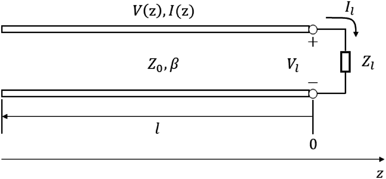

Similarly, the total current on the line is described by

The total voltage and current at the load are related by the load impedance, so at

The amplitude of the reflected voltage wave normalized to the amplitude of the incident voltage wave is known as the voltage reflection coefficient,

Among them, the characteristic impedance
In addition, according to the definition of return loss

From the above formula, it can be seen that the terminal load

From the VNA testing of
Preparation and performance evaluation of microstrip line
In order to verify the feasibility of calculating the characteristic impedance of the microstrip line by
Design of conductor strips for fabric-based microstrip line with a certain characteristic impedance
In order to obtain the microstrip line with a certain characteristic impedance, conductor strips must be designed according to the dielectric constant and thickness of substrate. As shown in Figure 2, the characteristic impedance can be expressed
11
: Schematic of microstrip line.

Among

For the microstrip line with a certain characteristic impedance

Among


In order to apply the microstrip line to common electronic devices, the characteristic impedance of the microstrip line designed in this work is 50 Ω. As shown in expression (10), the width of the conductor strip can be obtained.
Design and fabrication of fabric-based microstrip line with a certain characteristic impedance
The polyester nonwoven fabric is used as the substrate, and was purchased from Shandong Jiantong Eng. Tech. Co., Ltd. (Dezhou, China) with a mass per unite area of 79 g/m2. Its thickness was measured according to GB/T3820-1997 standard (Determination of thickness of textiles and textile products) by fabric thickness gauge (YG141N, China). Its single-layer thickness is 0.716 ± 0.018 mm. Polyester sewing thread 40s/3 was used and obtained from Ningbo Guman Textile Co., Ltd. (Yinzhou, China). The silver-plated nylon multifilament yarn was used for embroidered conductive lines. It was purchased from Qingdao Hengtong X-silver Specialty Textile Co., Ltd. (Qingdao, China). The copper foil has a thickness of 0.05 mm and was from Dongguan Xinshi Materials Co., Ltd (Guangzhou, China).
In this study, split post dielectric resonator technique was used to measure dielectric properties of the fabrics.13,14 The test process was based on the method of IPC TM 2.5.5.13 (Relative Permittivity and Loss Tangent Using a Split-Cylinder Resonator) test standard, and its dielectric constant and dielectric loss tangent are 1.134 and 0.00137, respectively. According to equations (10) and (12), if the substrate is the single-layer fabric, the width of the conductor strip is 3.197 mm. Due to the limitation of production accuracy, the width of the conductor strip is set to 3.20 mm. The theoretical characteristic impedance is 49.76 Ω from equations (8) and (9), which is close to 50 Ω. For the two-layer fabric used as substrate, its dielectric constant and dielectric loss tangent are the same as that of single-layer fabric.15,16 Therefore, if the substrate is the two-layer fabric, the width is set to 6.40 mm and its theoretical characteristic impedance is 49.76 Ω. In addition, the length of microstrip line was set to 52.00 mm, which has no effect on its impedance.
Design and fabrication of fabric-based copper foil microstrip line
In order to verify the feasibility of calculating the characteristic impedance of the microstrip line by
First, the single-layer polyester non-woven fabric was used as the substrate. As mentioned above, the width as well as the length of conductor strip are designed to 3.20 mm and 52.00 mm, respectively, and the theoretical characteristic impedance of its microstrip line is 49.76 Ω. Then, the fabric-based copper foil microstrip line was fabricated. It refers to a microstrip line formed by a fabric substrate, a copper foil conductor strip and a ground plane, shown in Figure 2. It is worth noting that the copper foil conductor strip was on the top, the fabric substrate was in the middle and the copper foil fixture used as the ground plane was at the bottom.
Design and fabrication of fabric-based embroidered microstrip line
Different from the structure of traditional conductor strip, the conductor strip of embroidered microstrip line is a conductor formed by the conductive yarns passing through the fabric. Thus, the conductive yarn passing through the fabric made it possible that the conductor strip was connected to the ground plane. It will cause a short circuit. In order to avoid forming a short circuit, it is necessary to add fabrics between the fabric embroidered with conductor strip and the ground plane. On the other hand, the stitch structure of the conductive yarn may affect the dielectric properties of the fabric substrate embroidered with conductor strip. Therefore, it is hard to determine the equivalent substrate formed by the fabric embroidered with conductor strip and the added fabric. In this work, after verifying the feasibility of calculating the characteristic impedance of the microstrip line by
The embroidered microstrip line with single-layer conductor strip is called single-layer embroidered microstrip line. The single-layer conductor strip refers to the conductive layer formed by the conductive yarn on the top and ordinary yarn on the bottom. The process of single-layer microstrip line embroidered by peripheral needle pattern was shown in Figure 3. First, the width of the conductor strip was calculated by equations (10) and (12) and its length was set to 52 mm, and their sizes were set through the embroidery CAD software. Then, the conductor strip is embroidered on the nonwoven fabric by a computerized embroidery machine (brother NV 950, Brothers (China) Commercial Co., Ltd.). Next, the fabric embroidered with the conductor strip and the extra nonwoven fabric were sewed together with the polyester sewing threads by the embroidery machine. Finally, the nonwoven fabric with the conductor strip was placed directly on the copper plate fixture to form a complete microstrip line. The related actual sample was shown in Figure 4. The formation of single-layer embroidered microstrip line. The schematic diagram of single-layer embroidered microstrip line actual sample.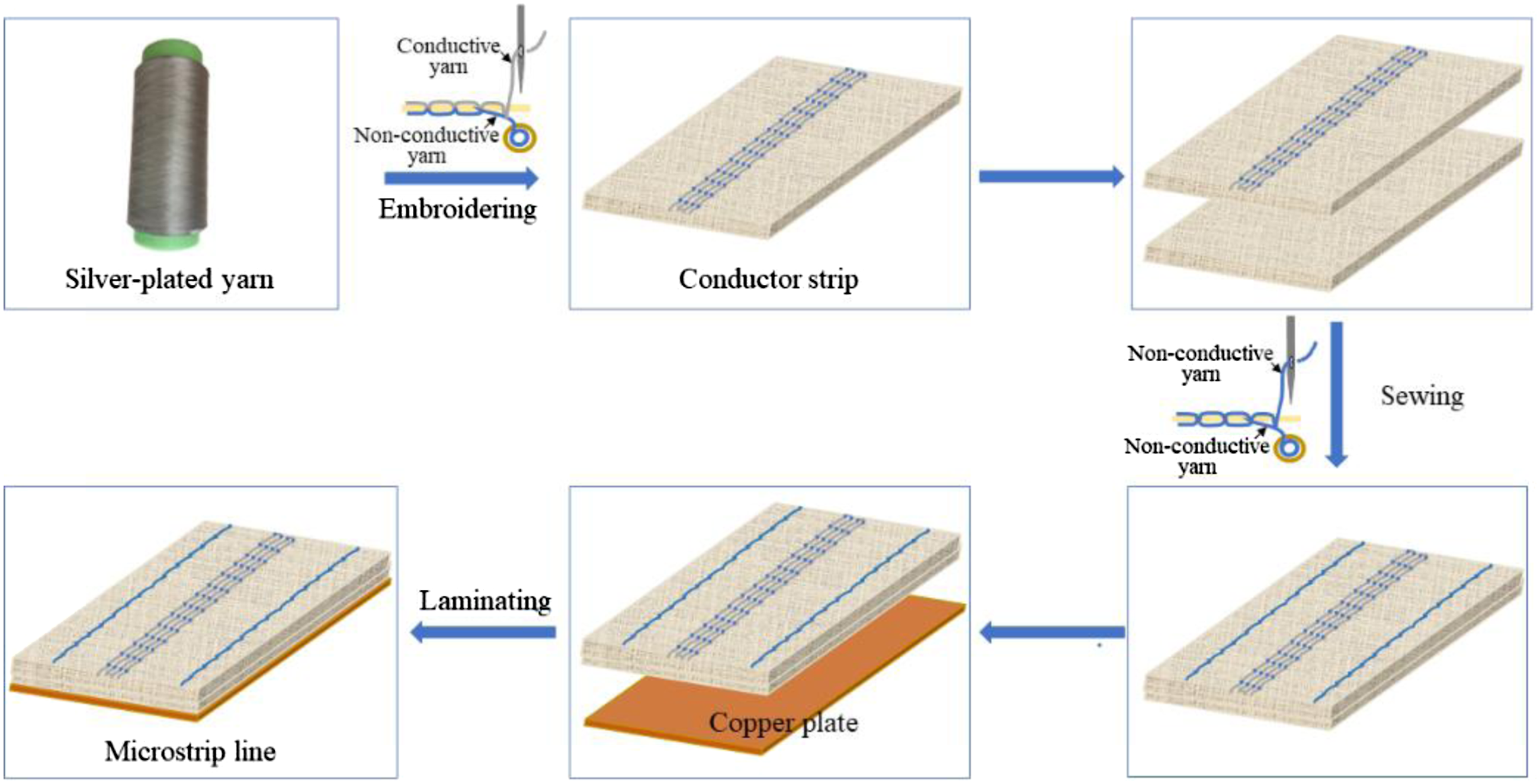

Similarly, the embroidered microstrip line with double-layer conductor strip is called double-layer embroidered microstrip line. The double-layer conductor strip is composed of the conductive yarns on the top and on the bottom. The cross-sectional view of two kinds of embroidered microstrip line were shown in Figure 5. It can be seen that conductive yarns of two kinds of conductor strips will be connected to ground planes to cause a short circuit. In order to avoid short out, it is necessary to add additional fabrics between the fabric embroidered with the conductor strip and the grounding plate, shown in Figure 5. Additionally, the stitch structure of the conductive yarn may affect the dielectric properties of the equivalent substrate. Therefore, an assumption is made for the equivalent substrate of single-layer and double-layer embroidered conductor stirp. For the single-layer embroidered conductor strip, single-layer fabric was added between the fabric embroidered with the conductor strip and the grounding plate. Its conductive yarn passes through the fabric, and its length exposed on the back of the fabric is very short and ignored. In this way, the equivalent substrate is two-layer fabrics formed by the fabric embroidered with conductive yarn and the additional fabric. For the double-layer embroidered conductor strip, its both sides are conductor. It is assumed that the fabric embroidered with double-layer conductor strip is not part of the equivalent substrate. Therefore, the equivalent substrate is the additional fabric. To be consistent with the equivalent substrate of single-layer embroidered microstrip line, two layers of nonwoven fabric are added between the fabric embroidered with conductor strip and the ground plate. The cross-sectional view of embroidered microstrip line (a) with single-layer conductor strip; (b) double-layer conductor strips.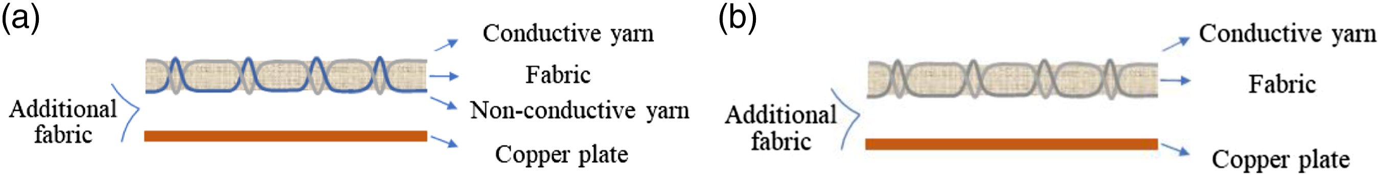
Based on above assumption, the equivalent substrates of two kinds of embroidered microstrip lines were both two-layer nonwoven fabrics. As mentioned before, to obtain a microstrip line with a characteristic impedance of 50 Ω, their widths are both set to 6.40 mm and the characteristic impedances of corresponding microstrip lines are both 49.76 Ω.
Performance test of fabric-based microstrip line
The performance test of the traditional PCB board microstrip line is that the two ends of the microstrip line was connected to two SMA connectors, connected to the two ends of the vector network analyzer VNA (Agilent E5071 C) through the coaxial line.
17
Different from the PCB rigid board, the fabric is flexible and fabric-based embroidered microstrip line is deformed easily when its microstrip performance was measured by traditional method. Then, the stability of measurement of transmission performance is poor. In order to solve this problem, the related scholars have proposed a fixture for fixing the embroidered conductor strip, which is composed of an FR4 board and a copper ground plate plated on the bottom.
18
Under the action of the fixture, the probe of the SMA connector has a good contact with the embroidered conductor strip and the fabric embroidered conductor strip could keep flat. The fixture can make the test stable and repeated. However, the fixture is made up of FR4 board and copper. In this way, the substrate is the fixed FR4 board and unchanged. In order to make the substrate flexible, the copper plate was proposed to replace the above fixture in this work, shown in Figure 6. The new fixture not only has the advantages of fixing the embroidered conductive strip and acting as the grounding plane, but also has the flexible substrate used as any material without limitation. The test diagram of fabric-based microstrip line on transmission performance.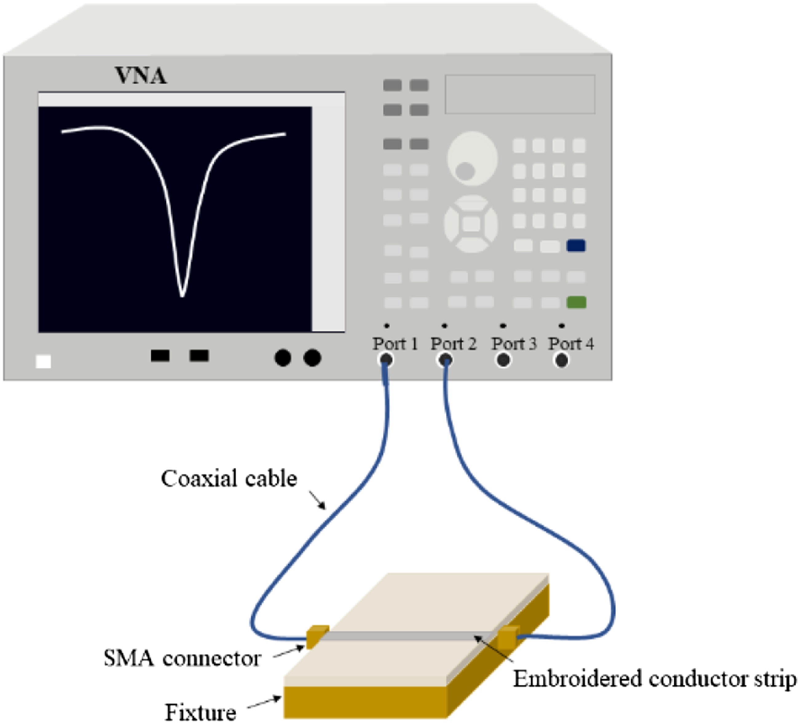
Before testing the embroidered microstrip line, the vector network analyzer VNA should be calibrated. First, the working frequency band was set to 100 MHz∼1 GHz, and the frequency sweep step was set to 1 MHz. Then, the full two-port calibration method SOLT that four calibration parts including short circuit, open circuit, load matching and straight through are used to calibrate the two parts, respectively, is used. Finally, as shown in Figure 6, the embroidered conductor strip was placed on the fixture and contacted with the two parts of the SMA connectors, which were connected to the vector network analyzer (VNA) Agilent E5071 C through a coaxial cable to test. Each sample was tested three times and their average value was taken.
Results and discussion
The relationship between the
and the characteristic impedance of microstrip line
The measured The measured and theoretical characteristic impedance of fabric-based copper foil microstrip line.
In order to verify the rationality of the characteristic impedance of the microstrip line calculated by using

The deviation rates between the measured and theoretical characteristic impedance of the fabric-based copper foil microstrip line were shown in Figure 8. It can be seen that the deviation rates fluctuate in the range of 8.41%–9.73% as the frequency changes. It means that the theoretical characteristic impedance of the fabric-based copper foil microstrip line is close to the measured values, and the characteristic impedance of the microstrip line could be obtained by using The error rate between the measured and theoretical characteristic impedance of fabric-based copper foil microstrip line.
The application of the calculation method of the characteristic impedance of microstrip line
The above results verify the rationality of the characteristic impedance of the microstrip line calculated by using
The determination of substrate for single-layer embroidered microstrip line
First, the calculation method of the characteristic impedance of microstrip line was used to determine the equivalent substrate of single-layer embroidered microstrip line. Based on above assumption, a single-layer conductor strip with the width 6.40 mm and the length 52 mm was designed to form the embroidered microstrip line with 50 Ω characteristic impedance. Taking a stitch spacing of 0.80 mm and a stitch length of 4.00 mm as an example to fabricate the conductor strip. The conductor strip with same embroidery parameters has three samples. Their measured and theoretical characteristic impedance are shown in Figure 9. Comparison of measured and theoretical characteristic impedance of single-layer microstrip line.
For the measured results, their small difference indicates that the characteristic impedance of the embroidered microstrip line has good repeatability. The difference may due to two factors: (1) the uneven thickness of nonwoven fabric; (2) the fluctuation of the actual width of the samples. In the above-mentioned assumption of single-layer conductor strip, if the assumption is true, the fabric embroidered with conductive yarn could be regarded as part of the equivalent substrate. The thickness of the equivalent substrate is the thickness of the double-layer nonwoven fabric (2*h). From equation (8), the theoretical characteristic impedance of the single-layer microstrip line can be obtained as 49.76 Ω. On the contrary, the fabric embroidered with conductive yarn is not regarded as part of the equivalent substrate. The thickness of the equivalent substrate is the thickness of the single-layer nonwoven fabric (h), and its theoretical characteristic impedance of the microstrip line is 29.47 Ω. As shown in Figure 9, it is obvious that the measure characteristic impedance curves of the three samples are closer to the theoretical characteristic impedance of 49.76 Ω. It indicates that the thickness of the equivalent substrate is the thickness of the double-layer nonwoven fabrics. Meanwhile, it shows that the assumption of the fabric embroidered with a single-layer conductive strip is regarded as part of the equivalent substrate is reasonable, so the effect of conductive yarns in the fabric on the dielectric properties of the equivalent substrate can be ignored. For the difference between the measured and theoretical characteristic impedance, on the one hand, the actual thickness of the nonwoven fabrics fluctuates with a certain range (the theoretical value), some of which are larger than their theoretical values and some of which are lower than their theoretical values. On the other hand, the widths of samples (7.03 mm, 7.01 mm and 7.12 mm) are larger than its theoretical values (6.40 mm), resulting in larger measured characteristic impedance than its theoretical values according to equation (8).
The determination of substrate for double-layer microstrip line
Similarly, the calculation method of the characteristic impedance of microstrip line was used to determine the equivalent substrate of double-layer embroidered microstrip line. Based on above assumption, the double-layer conductor strip with the width 6.40 mm and the length 52 mm was designed to form the embroidered microstrip line with 50 Ω characteristic impedance. Taking a stitch spacing of 0.80 mm and a stitch length of 4.00 mm as an example to fabricate the conductor strip. The conductor strip with same embroidery parameters has three samples. Their measured and theoretical characteristic impedance are shown in Figure 10. Comparison of measured and theoretical characteristic impedance of double-layer microstrip line.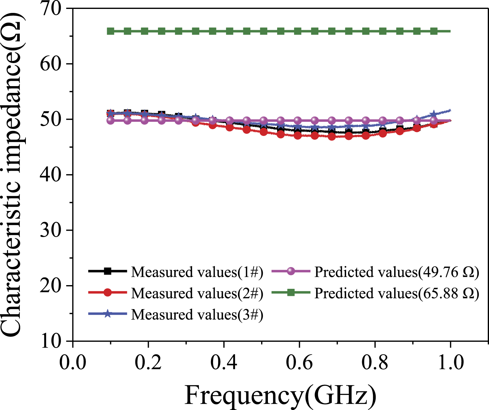
There is small difference between the measured results, and it indicates that the characteristic impedance of the embroidered microstrip line has good repeatability and stability. The difference may due to the uneven thickness of nonwoven fabric as well as the fluctuation of the actual width of the samples. In the above-mentioned assumption of double-layer conductor strip, if the assumption is true, the fabric embroidered with conductive yarn could be not regarded as part of the equivalent substrate. The thickness of the equivalent substrate is the thickness of the double-layer nonwoven fabric (2*h). From equation (8), the theoretical characteristic impedance of the single-layer microstrip line can be obtained as 49.76 Ω. On the contrary, the fabric embroidered with conductive yarn is regarded as part of the equivalent substrate. The thickness of the equivalent substrate is the thickness of three-layer nonwoven fabric (3*h), and its theoretical characteristic impedance of the microstrip line is 65.88 Ω. As shown in Figure 10, it is obvious that the measure characteristic impedance curves of the three samples are closer to the theoretical characteristic impedance of 49.76 Ω. It indicates that the thickness of the equivalent substrate is the thickness of the double-layer nonwoven fabrics. Meanwhile, it shows that the assumption of the fabric embroidered with double-layer conductive strip is not regarded as part of the equivalent substrate is reasonable, so the effect of conductive yarns in the fabric on the dielectric properties of the equivalent substrate cannot be ignored. For the difference between the measured and theoretical characteristic impedance, the actual thickness of the nonwoven fabrics fluctuates with a certain range (the theoretical value), some of which are larger than their theoretical values and some of which are lower than their theoretical values. Additionally, the widths of samples (7.02 mm, 6.85 mm and 6.79 mm) are than its theoretical values (6.40 mm), resulting in larger measured characteristic impedance than its theoretical values according to equation (8).
Conclusion
This work presents a method for calculating the characteristic impedance of a microstrip line. The results show that the characteristic impedance of the microstrip line can be accurately calculated through its
Footnotes
Declaration of conflicting interests
The author(s) declared no potential conflicts of interest with respect to the research, authorship, and/or publication of this article.
Funding
The author(s) disclosed receipt of the following financial support for the research, authorship, and/or publication of this article: This research was supported by the Fundamental Research Funds for Jiaxing Nanhu University (QD61220026).