
Abstract
Having control on the specific area of power harvesting devices is the main controllable parameter in their fabrication. Hence, in this paper, at first a piezoelectric nanofiber is made with different dimensions and all kinds of function tests including X-ray diffraction, Fourier transform infrared spectroscopy, differential scanning calorimetry are implemented thereon. After ensuring accurate …… responses from the device, some kinds of forces like concentration impact and distributed impact and tension creation by applying bending force are applied on the fabricated device in the laboratory. To assess the effect of electrode position, electrodes were placed in five modes within the samples and the output voltage was recorded with regard to applied forces type. The results indicated that an increase in specific area of nanofibrous mats in devices absolutely resulted in an increase in electric output, but the electric output reduced consequently when it normalized to the specific area of nanofibrous mats. These results imply promising approaches, as an enhanced efficiency energy-scavenging interface, for designing and fabricating various wearable self-powered electrical devices and systems.
Introduction
Small source of energies are largely available around us. While being small when considered separately, the total of these energies can be considerable [1]. Self-powering systems with the capability of harvesting energy from the environment are an attractive option for use in sensors, defense technology, and personal electronics [2,3]. This is actually important for small devices and low power consumption [4–7]. Self-powering of electronic devices by integrating a power generator that can scavenge and turn the surrounding local energy (e.g. mechanical, thermal, or chemical) into electrical energy to drive the electronic devices sustainably without any other electrical input has emerged as a viable solution. Piezoelectric materials are one of the most important materials used for harvesting energies and many studies have been conducted on them mostly presenting different approaches of power harvesting using piezoelectric materials and securitizing the analysis of power output for nano–macroscale piezoelectric energy harvesting systems [8–15]. Some researchers fabricated piezoelectric harvesting of mechanical energies using inorganic semiconductive nanowires (GaN, CdS, ZnO, ZnS, and InN) with a significant improvement comparing to the previous studies [16–21]. These nanowire-based electrical generators have shown the ability of converting mechanical energy from acoustic and ultrasonic vibrations and body movements into electrical energy, interestingly [22–24].
In comparison to nanowires, polymeric fibers are much suppler and flexible. They have higher strain level, and therefore can resist more mechanical deformation [1]. Polyvinylidene fluoride (PVDF), due to its high flexibility, biocompatibility, and low cost, is one of the most popular piezoelectric polymers. These features make PVDF as a worthy choice for energy transmutation applications including Micro electronic devices, actuators, and energy harvesters [25,26]. Recently, numerous papers have reported the use of electrospinning to fabricate PVDF nanofibers as a harvesting energy device [27]. Single PVDF nanofiber has been entrusted across a couple of electrodes by a near-field electrospinning process to harvest slight mechanical vibration [28] even though, the ensuing nanogenerators only showed very low piezoelectric outputs (up to 30 mV and 3 nA) [1,24]. Randomly oriented electrospun PVDF nanofiber webs and aligned nanofibers mats are another form of flexible devices for mechanical-to-electrical energy conversion. Difference between the single nanofibers and nanofiber mats is electric potential that formed along the fiber and across the nanofiber membrane thickness, respectively [27,28]. PVDF is a semicrystalline polymer that has four crystalline phases: α, β, γ, and δ. The nonpolar α-phase is generally found in commercially available films, polymer solution, and melting form. In this phase, the dipole moments have a random orientation, for this reason they cancel each other out put. Dipole moments pointing have the same direction in β-phase; thus, this phase is liable for the piezoelectric attributes of PVDF [25]. To achieve the desired piezoelectric properties in PVDF, high β crystal should be formed [1]. Usually, the later is accomplished by mechanical elongating along with an electrical poling treatment [29]. It is well documented that there is no need of additional poling treatment in case of the near field electrospun PVDF nanofibers [30]. Also, randomly oriented electrospun nanofiber mats can be directly used to make a piezoelectric power generator without any extra poling treatment [28].
The main reason for getting the β-phase form of the PVDF nanofiber mats goes back to the physical and electrostatic forces applied to the polymer droplet due to electrospining process. When a droplet of the solution is subjected to an electric field, the high applied voltage leads the drop into an elongated cone. In this process, charges applied to the droplet provides a stretching force to a collector where is a potential gradient. This mechanism ensures the fibers polarization, the morphological and crystalline structure of the fibers changes, and the β-phase forms within the structure of the fibers. Several parameters have influence in the morphology of the electrospun fibers and their properties. These parameters can be divided in three main groups: initial polymer solution (polymer in solvent percentage, type of the solvents, their volumetric percentage, and so on), process parameters such as jet formation, applied voltage, working distance, feed rate of the solution, and finally the environment condition (temperature, relative humidity). At first, these parameters were optimized to achieve the proper morphological properties of the electrospun fibers, which are reported in elsewhere [3,31,32].
Although the feasibility of harvesting the energy from the PVDF membranes is investigated in the literature, the effect of different structural properties on electrospun PVDF nanofiber membranes should be scrutinized. In previous reports [18,19,21,24,33–37], however, under comparable bending conditions, the current outputs of devices produced with such devices are less than 5 nA and the voltages are in the range of 1–20 mV. Because of the critical dependence on residual charges on the fibers in the gap between the nanofiber device and conductive electrodes, it is hard to make a device with the requirements of a realistic device. Therefore, in this research due to the importance of the electrode position and finite variation of dimensions in the nanofibrous-based nanogenerators, an experimental assessment of the effect of changes of electrode position and finite variation of dimensions in output electric voltage of a piezo/triboelectric nanofiber-based power harvesting device were performed.
Materials and methods
Materials
Poly(vinylidene fluoride) (PVDF) pellets with molecular weight viscosity of 46,000 (g mol−1) were purchased form Sigma-Aldrich. The solvents used in this work were N,N-dimethylformamide (DMF, Merck Chem. Co.) and acetone (Merck Chem. Co.). All the materials were used without further purification.
Preparation of piezo/triboelectric nanofibers mats and film
Electrospinning of nanofibers was performed in a horizontal electrospinning setup (Fanavaran Nano-Meghyas Company – IRAN, Figure 1). It consists a syringe positioned horizontally with its needle, a precisely controlled syringe pump, a high voltage power supply capable of 0–25 kV, and a grounded collector. Upon applying the high voltage, a fluid jet was ejected from the tip of the needle. As the jet accelerated toward a target, which was placed at 15 cm from the syringe tip, the solvent evaporated and nanofibers were collected on an aluminum foil substrate. Mass flow rate of the solutions was 0.5 mLh−1 to produce uniform nanofiber mats. Electrospinning was performed by a 1.0-ml plastic syringe tipped with a 22-gauge stainless steel needle. The positive lead from a high voltage supply connected to the metal needle, with the applied voltage of 18 kV. A cylindrical drum collector (outer diameter 26 cm) wrapped with aluminum foil substrate, with some modification to be able to put the conductive electrodes on it during the electrospinning, was used as the collector. The distance between the needle tip and the collector was 15 cm, and rotational speed of collector was 400 r/min. These parameters were selected from our previous activities [3,31,32].
Schematic view of electrospinning set-up used for fabrication of nanofiber samples. (1) Pump, (2) syringe, (3) high voltage, (4) ground connection (GND), (5) Taylor cone, (6) draft zone, (7) frame of collector, and (8) rotary collector.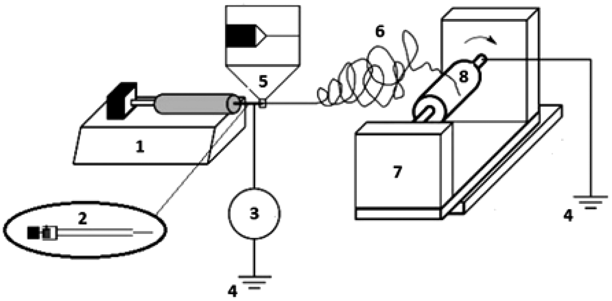
Fabrication of power harvesting devices
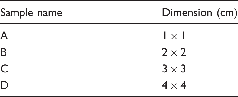
To fabricate a nanofiber-based power harvesting device, some modifications were made on the collector of electrospinning apparatus to collect nanofibers on the provided aluminum electrodes (two pieces of thin aluminum tape). A small piece of PVDF nanofiber mats (thickness 120 µm) in different surface areas was used as an active layer. An ordinary paper frame was set just outside the nanofiber mat enabling the bent nanofiber web to effectively recover to its original structure. This paper-based frame helped the nanofiber mats to keep its original shape during the test, since the paper has a reasonable bending rigidity compared with the electrospun nanofiber mats. Paper frame also helped to keep away from environmental noises due to covering the aluminum electrodes from the environment. The whole device was then sealed using a commercial paper tapes (Figure 2). Different dimensions of power generator are shown in Table 1.
(a) Schematic structure and (b) photo of an actual of the nanofibers generator device [3]. Dimension of power generator.
Characterization
Scanning electron microscopy (SEM) images were used for characterizing the microstructure and the morphology of the fabricated nanofibers (SEM, model: XL30; Philips Co.). All samples were gold coated (Bal-Tec. SCD50 sputter coater), and the images were taken at an acceleration voltage of 20 kV. The fiber diameter was measured using image processing software (ImageJ; National Institutes of Health, USA). Nanofibers crystalline structure was studied by X-ray diffraction (XRD, EQuinox 3000 model; INEL France Co.) using Cu-Kα radiation (wavelength 0.154 nm), and the samples were analyzed at room temperature. Fourier transform infrared spectroscopy (FTIR) spectra of PVDF nanofibers were documented by Spectrometer (model: NEXUS 670; Nicolet Co.) over a range of 400–4000 cm−1. Melting temperature (Tm) and melting enthalpy (ΔHm) of electrospun nanofibers were measured with differential scanning calorimeter (model: DSC 2010; TA Instruments.co) at a heating rate of 20℃ min−1.
Performing functional/structural tests on the samples of made piezo/triboelectric nanofibers
Morphology
Since well and steady piezoelectric properties come from uniform nanofiber mats, optimizing the electrospinning process is necessary. SEM images were used to study the morphology and structure of produced mats. SEM photographs of PVDF nanofiber mats (Figure 3(a)) with average diameter 124 nm and fiber diameter distribution (Figure 3(b)) are shown in Figure 3. As it is clear, nanofiber mats without structural defects were produced and selected for device fabrication.
Scanning electron micrograph (a) and fiber diameter distribution (b) of the selected nanofiber mats for nanogenerator device fabrication.
XRD analysis
XRD analysis patterns provide information on the long-range order and the crystal structure of random networks. As shown in Figure 4, the XRD patterns reveal the coexistence of both α- and β-phases in the samples. The XRD curves show a typical β crystal phase peak at around 2θ = 20.5°, which is assigned to the total diffraction in (110) and (200) planes [15,22–24]. This notice was confirmed by the XRD pattern in Figure 3. The peak at 40° corresponds to the reflection of the (020) plane of the α-phase. This peak (α-phase) reduced in intensity for electrospun membrane compared to the PVDF films produced with DMF solvent. This suggests that less α-phase and more β-phase crystalline structure is formed during the electrospinning.
X-ray diffraction patterns for (a) electrospun PVDF nanofiber mats and (b) PVDF film.
FTIR analysis
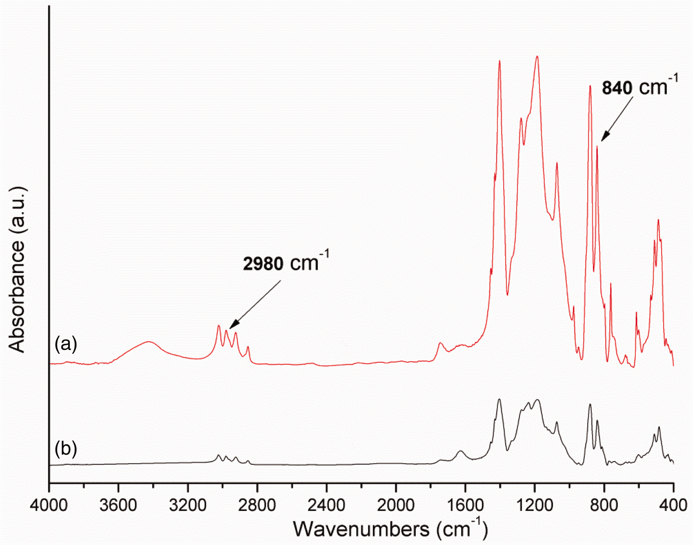
The FTIR spectrum of the nanofiber mats shows vibration peaks at 840 cm−1 and 1280 cm−1 (Figure 4), which are typical vibration characteristics of the β crystalline phase according the previous research and finding [34,38–42].
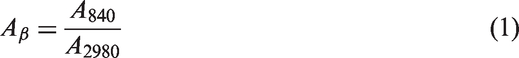
The content of β-phase was characterized by the absorbance ratio Aβ of the FTIR absorption peaks at 840 cm−1 and peaks at 2980 cm–1 based on equation (1) [43].
From XRD and FTIR results, it has been revealed that the film has weaker β-phase crystalline than electrospun nanofibers mats. Therefore, it can be conferred that to create piezoelectric properties, electrospinning process brings the formation of β-phase crystalline in PVDF membrane without need to post treatment (e.g. drawing, annealing, etc.).
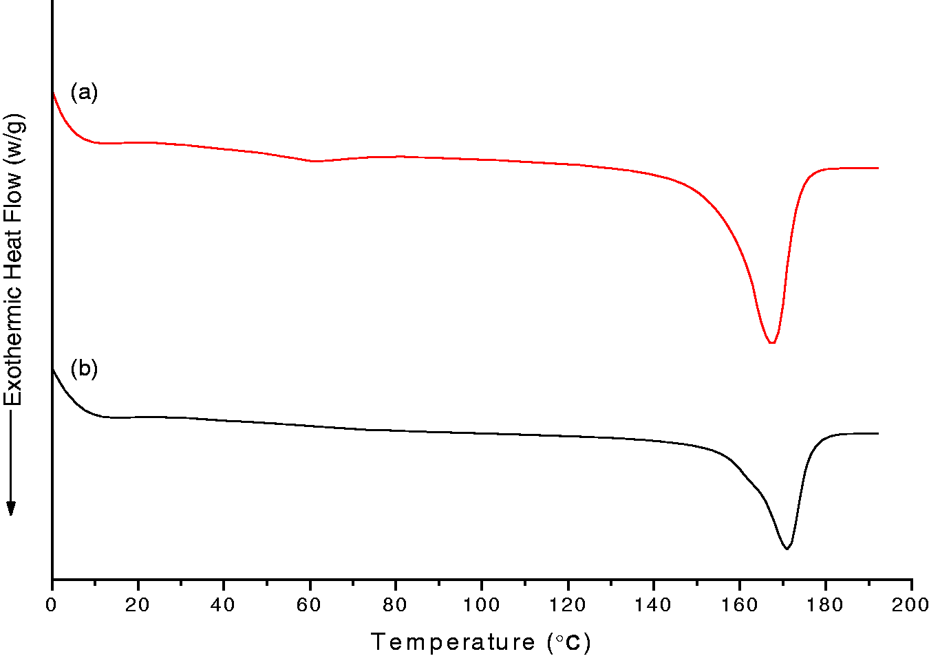
Differential scanning calorimetry analysis
Figure 6 presents differential scanning calorimetry (DSC) melting traces of electrospun PVDF nanofiber mats and granule. The melting temperature (Tm) of PVDF granules Figure 6-b: 170.96 C is more than nanofibers Figure 6-a: 167.45 C. The crystalline structure at the higher temperature region is the sign of α-phase formation, while at the lower one is the sign of β-phase formation [33]. Also, the melting point of β-phase is less than the melting point of α-phase [39]. It can also be seen from Figure 5 that the melting enthalpy of PVDF nanofibers FTIR spectra for (a) PVDF film and (b) electrospun PVDF nanofiber mats. DSC thermograms: (a) electrospun PVDF nanofiber mats and (b) PVDF granules (with heating rate of 20℃ min−1).
Trial steps of evaluating fabricated piezo/triboelectric nanofibers devices
According to the results obtained from previous section and ensuring from accurate respond of fabricated piezo/triboelectric nanofibers, to assess the effect of changes on electrode position and finite variation of its dimension on the output voltage, an auxiliary circuit was used which electrical current amplified 1000 times more and voltage 40 times more and this voltage was measured by oscilloscope.
Amplitude impedance
First, the amplitude impedance of the fabricated device was calculated via applying different frequencies (70 Hz to 20 kHz) by using an impedance analyzer (Figure 7). This behavior indicates that the piezoelectric device (consisting of nanofiber mats and two electrodes) has an acceptable capacitance property.
The experimental amplitude impedance evaluation of electrospun PVDF nanofibers mats as a function of frequency at room temperature.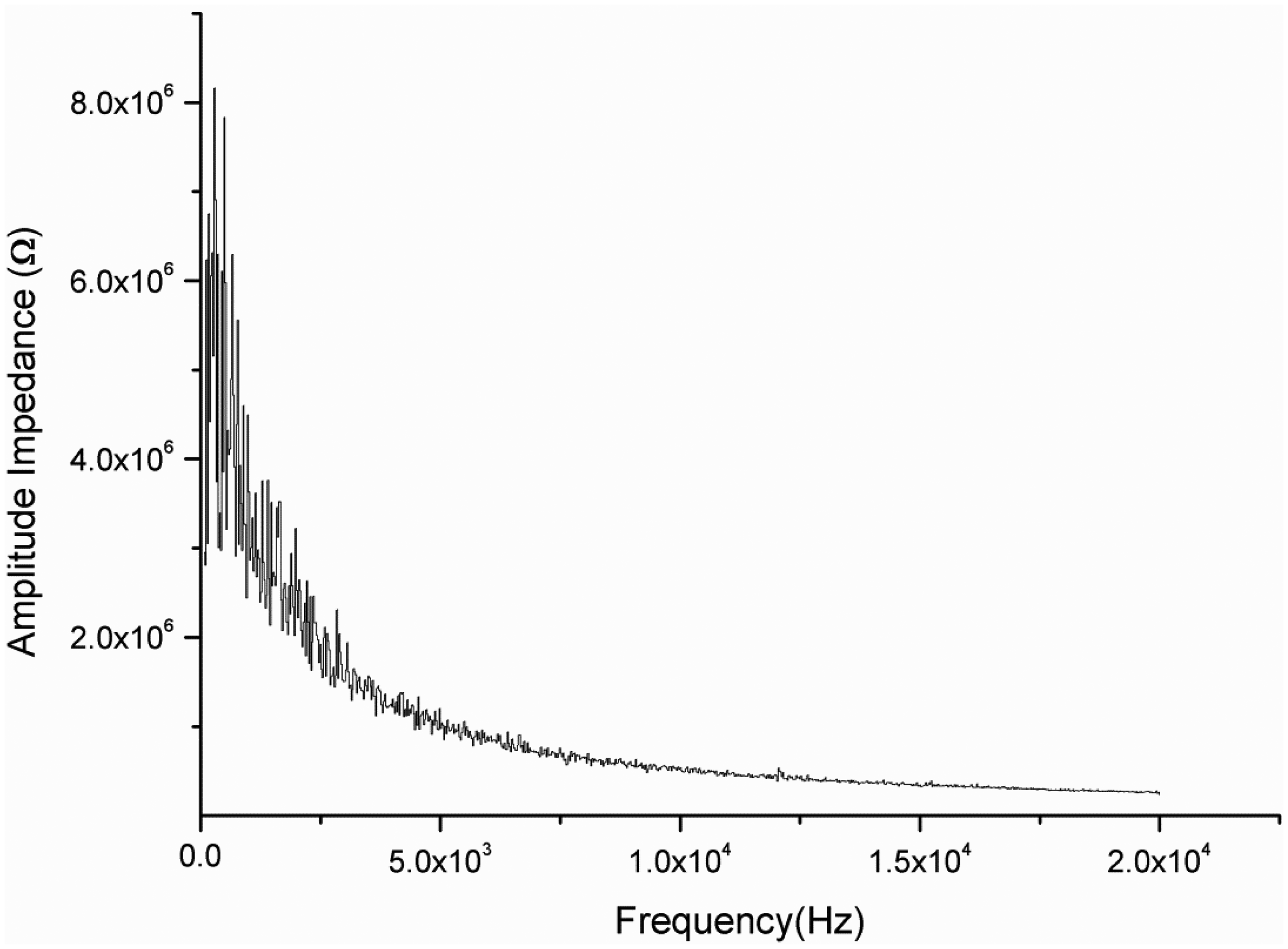
Procedure of applying mechanical tension on the fabricated devices
Applying impact force
Impact force is resulted from releasing a 50 -g weight bulb from a height of 15 cm that was applied on the samples in two modes. In the first mode, the impact is applied centralized on a point and in the second mode, a force was applied to the samples through a uniform stiff layer to distribute the applied force throughout the area as a distributed impact to involve the whole surface of samples. Results obtained in this experiment are provided in the result section.
Applying bending force
In order to use tension as stimulation applying factor, bending was used to stimulate the samples. Samples with the frequency of 30 times per minute (0.5 Hz) were bended by hand.
Procedure of electrode placement in the devices
To assess the effect of electrode location, electrode was placed in five modes in the fabricated samples made from piezo/triboelectric nanofibers and then the output voltage was measured after applying different forces. At the first mode, electrode was placed at the center of sample and four other modes of electrode placement will be in accordance with the areas shown in Figure 8.
Different modes of electrode placement in the samples.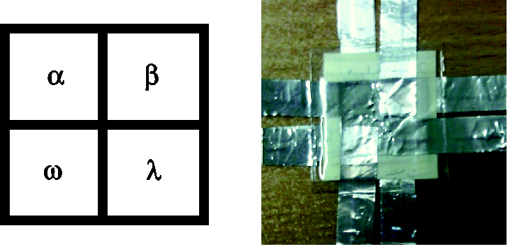
Results
Electrical voltage output of piezo/triboelectric nanofibers layers with different dimensions and modes of electrode placement in the samples.
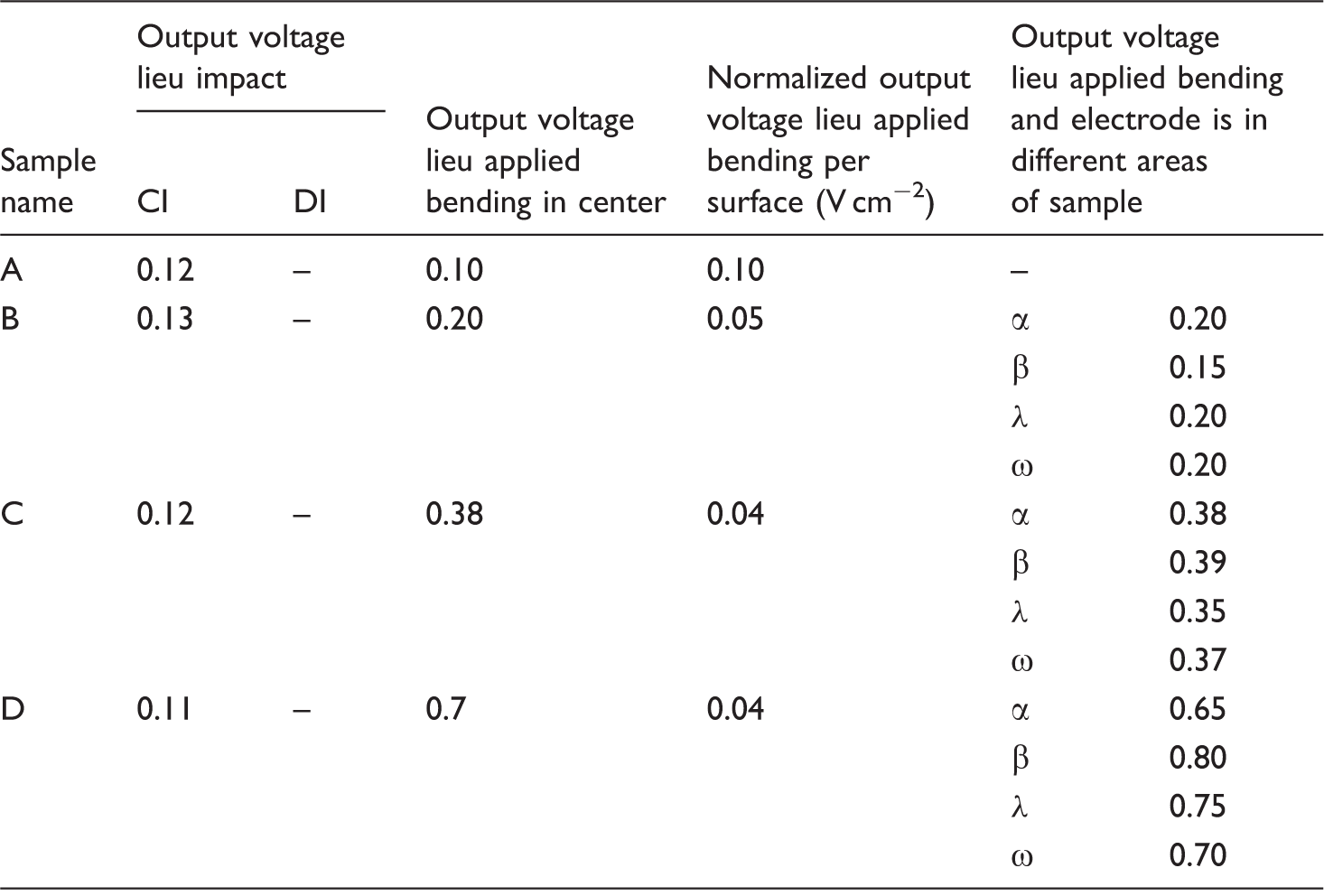
CI: concentration load impact; DI: distributed load impact.
As it can be conferred from Table 2 and Figures 9 and 10, increase in electrode area absolutely results in increase in electric output, although it was reduced when results normalized to the area. Considering fixed value of applied tension, the tension applied on a point of an area with smaller dimensions is more than an area with larger dimensions. In the same concept, large dimension, area uniformity (in the light of participation of piezoelectric nanofibers in electric output or in other word, uniformity of layer thickness in microscopic vision) was reduced that may be referred to the nature and limitation of production process of nanofibers (electrospinning process). In this mode, the whole area is covered by an electrode.
Electric output vs. sample area. Normalized output on the surface vs. the sample area.

Table 2 shows that the electric output has no significant difference for different electrode placement areas. In other words, it has been shown that the electric output is independent from electrode placement.
Conclusions
In summary, the present results show the possibility of designing and fabricating various wearable self-powered electrical devices and systems using engineering the electrospun PVDF mats as a fibrous and wearable electrode. By controlling the crystalline phases along with other physical properties of nanofibrous mats, power harvesting devices with high sensitivity could be achieved. Results showed that an increase in electrode area absolutely results in increase in electric output, although it was reduced when results normalized to the area. Furthermore, the electric output of nanogenerator is independent from electrode placement within the fabricated devices. Consequently, several factors, including fiber alignments, fiber diameter distribution, electrospinning parameters, and position of the electrodes and their specific area, should be taken into account in designing and fabricating the power harvesting devices.
Footnotes
Declaration of Conflicting Interests
The author(s) declared no potential conflicts of interest with respect to the research, authorship, and/or publication of this article.
Funding
The author(s) disclosed receipt of the following financial support for the research, authorship, and/or publication of this article: The support provided by the ATMT Research Institute, Amirkabir University of Technology and INSF (Grant No. 92036082), and ARA Pazhohesh Co. are highly appreciated.