
Abstract
This study, for the first time, presents the growth, nucleation, and characteristics of TiAlSi thin films sputtered from a partially sintered Ti30Al16Si10 (at. %) composite target under controlled conditions of target power. The TiAlSi thin films were grown on soda-lime glass substrates through Direct Current (DC) sputtering at varying levels of the target power: 73.2 W, 151.2 W, and 269.5 W. The other deposition parameters: the deposition temperature, time, argon mass flow rate, substrate rotation, and deposition pressure, were kept constant at 23 °C, 150 min, 25 sccm, 5 rpm, and 10−3 mbar, respectively. The pre-sputter power, argon flow rate, and time were also kept constant at 73.2 W, 20 sccm, and 5 min, respectively. The physical properties, microstructure, crystal structure, topography, and mechanical properties of the thin film coatings were analysed. The thickness and rate of deposition of the TiAlSi thin films increased with an increase in the target power (73.2 W – 269.5 W) from 414.6 nm and 0.046 nm/s to 1358.8 nm and 0.151 nm/s, respectively. The chemical composition of all the thin films remained constant, with the formation of a uniform TiAlSi alloy with no segregation of elements. However, a thin (wetting) interlayer consisting of Si and O elements was observed between the TiAlSi layer and the glass substrate. Further, the structure sizes and roughness values of the TiAlSi thin films increased with an increase in the target power, with a maximum of 75.4 nm for the size and 4.78 nm for the RMS roughness of thin films deposited at the maximum target power (269.5 W). Lastly, mechanical analysis of the TiAlSi thin films depicted an increase in the hardness as the target power increased, with the highest hardness at maximum power (269.5 W) obtained as 4.76 GPa. Despite having the lowest elastic modulus (50.5 GPa), the coating deposited at the highest power exhibited the highest plasticity index (H/E) and plastic deformation factor (H3/E2) of 0.094 and 0.042 GPa, respectively, which indicated the high resistance to abrasive wear, cracking, and deformation, compared to thin films deposited at the lowest target power (H/E = 0.066 and H3/E2 = 0.015 GPa). This study demonstrates that target power is a significant factor in determining the growth of TiAlSi thin films during the sputtering process and can be used for better control of their physical, structural, and mechanical properties.
Introduction
Titanium-based thin films have attracted applications in various fields ranging from the mechanical shielding of surfaces to medical applications. This is owed to their high hardness, strength, fracture toughness, corrosion resistance, and durability. Additionally, these coatings, when coupled with other elements such as aluminium, silicon, silver, and nitrogen, have been shown to improve the surface performance of mechanical elements under high shear forces and areas susceptible to oxidation and corrosion. 1 To tune the behaviour of the thin films for these (and other) applications, precise control of the deposition process and parameters towards the growth of thin films offers significant benefits in the formation of dense, hard, and functionally desirable thin films. Target power is one of the most significant parameters in the sputtering process. Target power influences the ionisation of the sputtering gas, which affects the plasma density in the deposition chamber. Plasma density significantly affects the number of sputtered and deposited atoms, which are closely associated with the rate of deposition of the thin films.
As such, different authors have evaluated the influence of power supplied to targets and substrates on the deposition and performance of titanium-based thin film coatings. For instance, Kavitha, Kannan, and Rajashabala 2 investigated the effect of target power on the physical characteristics of Ti thin films prepared through supported discharge magnetron sputtering. It was observed that an increase in the target power (60–120 W) led to a change in the crystallinity of the coatings and the crystal size. The coatings prepared in triode (traditional diode mode fitted with an additional hot filament) and diode modes of the DC magnetron system exhibited increases in the grain size up to a maximum of 80 nm and 5 nm, respectively. In another study, Chen et al. 3 studied the evolution, microstructure, and performance of TiAlSiN coatings deposited on Si(100) substrates using pulsed power magnetron sputtering under different peak power settings (24.8–56.8 kW). The authors noted that the microstructure of the coatings changed from a columnar structure to a grassy-like structure with an increase in the deposition power. The hardness (23.6–31.6 GPa) of the TiAlSiN thin films increased significantly with the peak power. No cracks were observed on thin films deposited at high power, which depicted the high fracture toughness of the thin films. 3
A similar study was conducted by Paksunchai et al. 4 on the effect of varying the current to the Cr target (0.4 A – 1.0 A) on the structural performance of (Ti, Cr)N coatings during the reactive unbalanced magnetron co-sputtering. These coatings were deposited on silicon wafers and glass slides using Ti and Cr targets. The coatings produced at different Cr target currents showed strong dominant orientations (111) whose intensity increased with the increasing target current. Considering the chemical composition, the authors realised that an increase in the current supplied to the Cr target, as expected, increased the Cr content in the coatings (from a ratio of 0.46 to 0.81) while the Ti content decreased from a maximum of 0.54 to 0.19. At equal target currents, the Cr content was higher than the Ti current, attributed to the high sputtering energy of Cr atoms as a function of their lower atomic radius (0.1249 nm) compared to Ti with 0.1445 nm. Further, Hernan et al. 5 studied the growth and characteristics of TiAlN thin coatings doped with Ag and Cu during DC magnetron sputtering. These coatings were deposited on stainless steel substrates under different contents of Ag and Cu. The addition of Ag-Cu was observed to reduce the hardness of the coatings while increasing the lubricity, which designated the usability of these coatings in tribology.
Consequently, Yang et al. 6 evaluated the influence of target power on the microstructure and development of TiN thin films grown through dual pulse power magnetron sputtering. The authors noted that changing the target power ratio in the first (Pw) and second (Ps) ionisation periods (Pw/Ps) from 0.9/1.6 to 0.3/2.2 increased the deposition rate of the TiN thin films from 26 to 61 nm/min. The change in the power ratio also improved the microstructure and hardness of the thin films. Moreover, Santiago et al. 7 evaluated the effect of target power on the optical and electrical characteristics of TiO produced through reactive grid-assisted magnetron sputtering. An increase in the target power was observed to decrease the optical gap and sheet resistance while increasing the optical gap entropy, optical absorption, and the thickness of the coating. More studies reporting the effect of the deposition power of titanium-based thin coatings are available in the literature.8–11
Other studies have reported the properties of thin films based on the TiAlSi thin films. For instance, Beresnev et al. 12 evaluated the structure and properties of multi-layered nitride coatings of Ti(Al)Si deposited through the vacuum-arc technique under varying conditions of the arc current, focusing current, substrate bias, pressure of the N2 atmosphere, and chemical composition with an introduction of Mo, Cr, and Zr metals. The authors noted a dense and droplet-free microstructure of the [Ti(Al)):Si]Nx coatings with an increased homogeneity on annealing. Further, an increase in the substrate bias (50 V to 110 V) and the pressure of the N2 atmosphere (10−5 to 4 × 10⁻³ Torr) in the deposition of the [Ti(Al)):Si]Nx slightly reduced the Ti/Al ratio from approximately 3.36 to 2.74 (before annealing), which translated to the deposition of the more stable AlN on the substrate. In contrast, the hardness of the films increased from about 6.65 GPa to 10.58 GPa, respectively. All the films exhibited an improvement in the micro-hardness after annealing. The authors furthered the study by evaluating the effect of varying the composition of the alternating layers of the (TiAlSiY)Mo/Cr/ZrN thin films. 13 A similar study was conducted by Pogrebnjak et al. 14 on the antibacterial effect of introducing Au into the (TiAlSiY)N/CrN thin film. The Au-based thin films displayed excellent inhibition against Gram-negative and Gram-positive bacteria with minimal surface contamination. Other similar studies have been reported in literature.15,16
Despite the availability of studies evaluating the deposition parameters and characteristics of Ti-based thin films, there are limited studies on the influence of target power on the evolution and growth of ternary TiAlSi thin films from a composite TiAlSi target during magnetron sputtering. Additionally, to the best of the authors’ knowledge, there are limited studies on the formation and properties of TiAlSi thin films, which form a key component of other Ti-based thin films, for instance, TiAlSiNx and TiAlSiNx/MeN (where Me could be a metal such as Mo, Cr, Zr, or Cr, among others), whose performance in high-strength applications is dependent on the base coating; TiAlSi. This study, therefore, for the first time, presents the growth, formation, and characteristics of TiAlSi thin films sputtered from a partially sintered composite target under variable conditions of target power. The thin film coatings were deposited on glass slides in a magnetron sputtering facility using a single composite target with titanium, aluminium, and silicon. These coatings were then investigated for their chemical composition, microstructure, topography, and mechanical properties. The findings of this study provide insights into the tuning of the properties of thin films prepared from composite targets, especially for high-strength applications.
Methods
Substrate preparation and deposition
Soda-lime glass slides were used as the substrates in the deposition. The glass substrates measuring 75 × 25 × 1 mm3 were ultrasonically cleaned in deionised water for 5 min and thoroughly cleaned in 1:5 Decon 90 solution for 30 s on each side. They were ultrasonically cleaned again for 10 min and then cleaned using isopropyl alcohol (IPA). The substrates were then dried using pressurised nitrogen gas. A thin strip of Kapton tape was applied across a section of the substrates to provide a step for measuring the film thickness. The substrates were then loaded onto the substrate holder at a target-substrate distance of 100 mm. A 99.99% pure composite Ti30Al16Si10 (at. %) circular target (50.8 mm diameter and 6.35 mm thick) was loaded onto the Direct Current (DC) magnetron of the nanoPVD benchtop magnetron sputtering system (S10, Moorefield Nanotechnology). The system is equipped with two magnetron assemblies: DC (used in this study and rated at a maximum current of 1.4 A) and Radiofrequency (RF). The RF magnetron was kept covered during the deposition process. Before each deposition, the target was pre-sputtered (soaked) for 5 min at a target power of 73.2 W and an argon gas flow rate of 20 standard cubic centimetres per minute (sccm) to remove any impurities and stabilise the sputtering process while shielding the substrates. Power supplied to the DC target was regulated by adjusting the percentage of the target current from 15% to 50%. The main deposition parameters are listed in Table 1.
Main deposition parameters.
Characterisation techniques
After each deposition, the system was vented to room pressure and the samples were recovered from the substrate holder. The thickness of the thin film coatings was measured in a standard scan using a surface profilometer (DektakXT, Bruker) equipped with a stylus radius of 12.5 µm, a force of 3 mg, a scan range of 6.5 µm, a scan resolution of 0.2 µm, a scan length of approximately 2 mm, and a scan duration of 30 s. The microstructure of each of the coatings was analysed using a field emission gun scanning electron microscope (FE-SEM, Tescan Mira3) fitted with an in-beam scanning electron gun and using a 6.0 kV power. The composition of the thin films was obtained via energy dispersive spectroscopy (EDS) using an XMax150 detector (Oxford Instruments) fitted onto the FE-SEM. The analysis was conducted under constant conditions of the electron beam voltage (5 keV), beam intensity (10), and working distance (15 mm) to ensure the interaction volume remained constant and to avoid influence from the glass substrate. The crystal structure of the TiAlSi thin film coatings was evaluated using X-ray diffraction (SmartLab SE, Rigaku) with the parameters listed in Table 2.
XRD parameters for the TiAlSi thin film coatings.
The topography of the coatings was assessed using atomic force microscopy (AFM) (Dimension edge 3100, Bruker) equipped with a silicon tip on nitride lever in the tapping force ScanAsyst Mode with an auto gain and setpoint setting, a peak force amplitude of 0.3 µm, a peak force frequency of 2.0 kHz, a lift height of −0.2 µm, a sync phase distance of 84°, an LP deflection bandwidth of 77.7 kHz, a detector voltage of approximately 2.5 V, and a ScanAsyst noise threshold of 0.05 nm. Two hundred fifty-six (256) line scans were conducted on the sample surfaces at a scan rate of 0.5 Hz on a scan range of 1 µm × 1 µm (scan area of 1 µm2) at ambient conditions with no rotation or offset.
Lastly, the hardness (H) and reduced Elastic modulus (Er) of the coatings were obtained through nanoindentation using a tribo-indenter (TI900, Hysitron) fitted with a Berkovich tip and taking 4 × 4 indentations per sample. A constant indentation force of 500 µN was applied, which kept the indentation depth ∼ 10% of the coating thickness to avoid interaction with the substrates (substrate effect). 17 A dwell of 10 s was allowed before unloading. The Elastic modulus (E) of the samples was computed using the model proposed by Oliver and Pharr. 18 The Young's modulus and Poisson's ratio of the indenter were taken as 1400 GPa and 0.07, respectively, while the Poisson's ratio of the thin films was taken as 0.25. 19
Results and discussion
Chemical composition
The average composition (in at. % and wt.%) of the TiAlSi thin films obtained from the EDX analysis of the samples deposited at varying target power is given in Table 3.
Composition of the TiAlSi thin films.
In addition to the expected elements in the TiAlSi thin films (Ti, Al, and Si), traces of oxygen (impurity) were detected (Table 3). For an increase in the target power at a constant interaction volume of the electron beam, no significant change in the chemical composition of the TiAlSi thin films was observed with a change in the target power. The average chemical composition of the TiAlSi thin films was obtained as 46.17 at. % (Ti), 16.95 at. % (Al), and 7.46 at. % (Si), which was consistent with the composition of the target used (with a negligible deviation). As shown in Figure 1, uniform TiAlSi thin films were formed with no segregation of the elements at all the target powers. The lack of segregation of elements showed the formation of the desired TiAlSi alloy through the sputtering process. 20
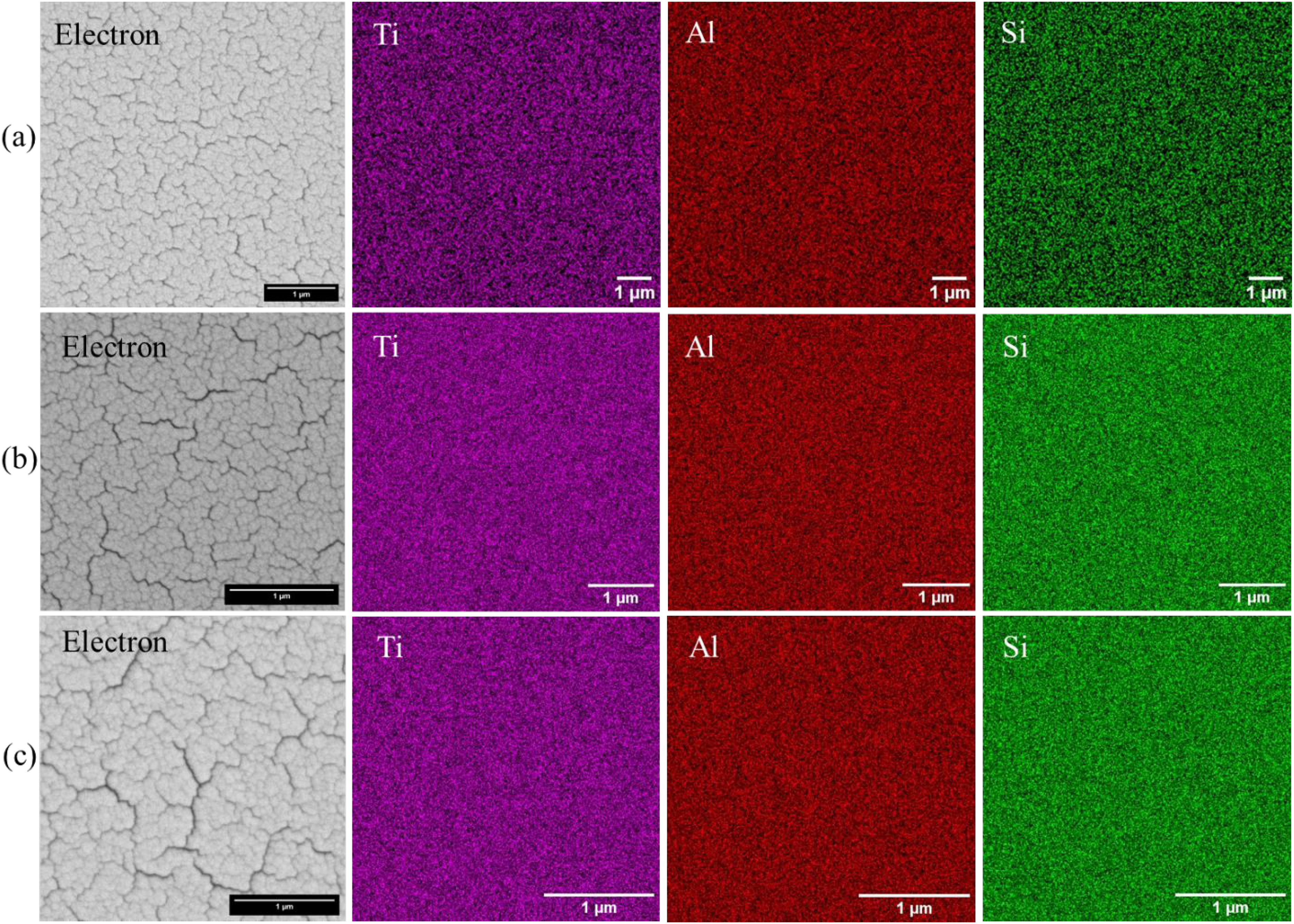
EDX analysis maps for the main elements of the TiAlSi thin films deposited at (a) 73.2 W, (b) 151.2 W, and (c) 269.5 W target power.
Additionally, a line scan was conducted across the cross-section of the TiAlSi thin films to evaluate the consistency of the composition of the elements as the films evolved from the substrate, as given in Figure 2 (a) and (b). From the top surface of the TiAlSi thin films (with a negligible amount of O2), the composition of the elements was observed to remain approximately the same across the cross-section of the thin films up to slightly above the substrate (Figure 2 (b)). A thin layer of silicon and oxygen was observed between the constant composition TiAlSi layer and the substrate in all the thin films (as shown in Figure 2 (a) and discussed later in microstructure analysis). This layer, where the composition of Si and O increased in Figure 2, was associated with the seeding of silicon in the soda-lime glass substrates to the thin film, leading to its early oxidation to form a probable oxide of silicon. 21 Moreover, owing to the low atomic radius of Si of 0.132 nm, compared to Ti (0.147 nm) and aluminium (0.143 nm), for the same sputtering target power, the sputtered atoms of Si travelled faster and at higher energy towards the substrate, reacting first with the oxide impurity in the substrates to form a thin oxide layer of silicon on the substrate.4,22 The TiAlSi thin film was then formed on top of this layer.
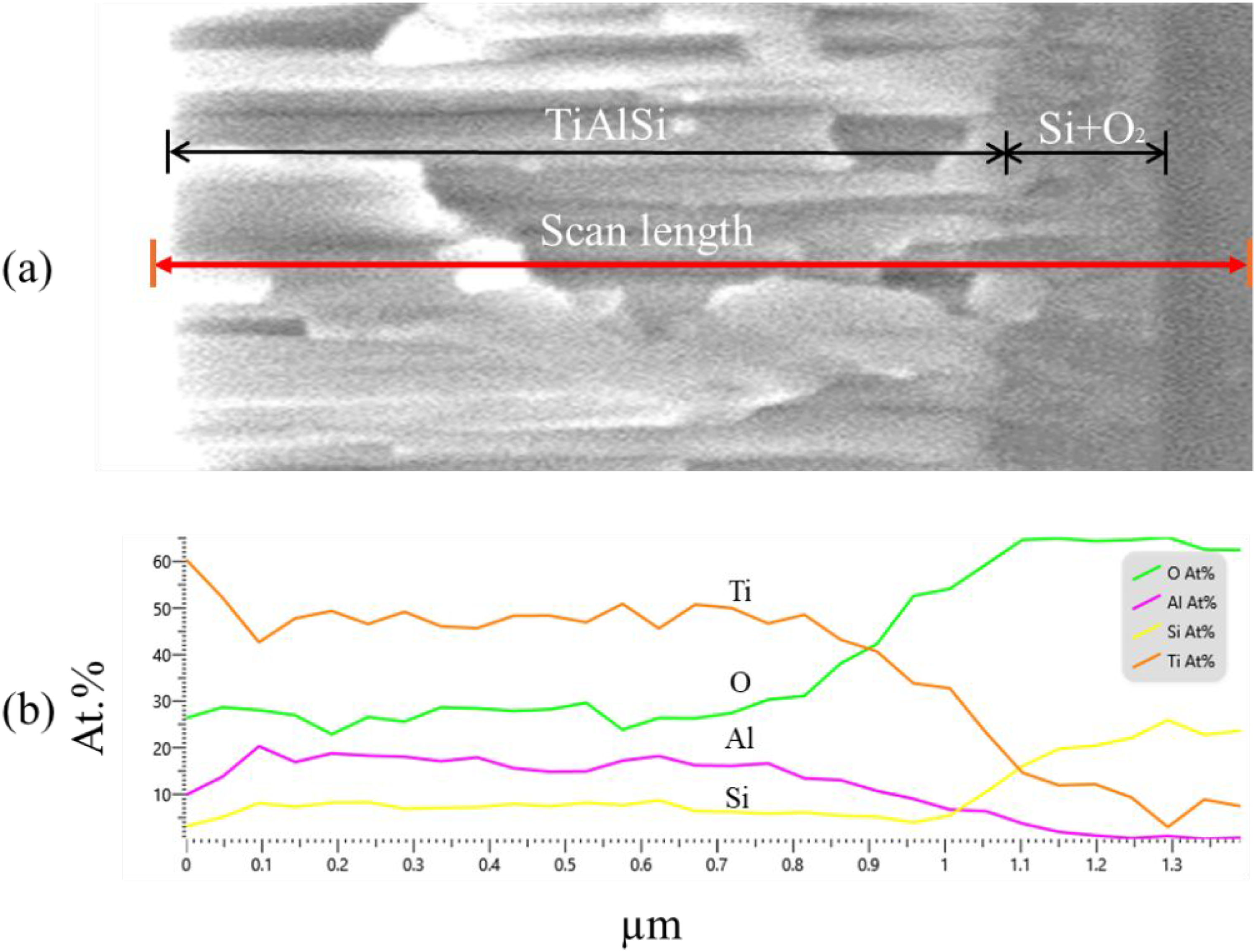
EDX analysis line scan of the TiAlSi thin films showing the formation and position of the tiAlSi layer and the Si + O2 layer.
Topography, microstructure, and crystal-structure
The coating thicknesses (Ct) with the standard deviation (S.D) and rates of deposition (Rd) for the samples deposited at different target powers are given in Table 4.
Coating thickness and rate of deposition.
An increase in the target power from 73.2 W to 269.5 W increased the thickness of the TiAlSi thin film coating from approximately 415 nm to 1359 nm, respectively. The P3/P1 ratio for the target power and coating thickness were 3.68 and 3.28, respectively. This ratio, with a difference of 0.4, indicates a close dependence of the TiAlSi thin film thickness on the target power applied. An increase in target power increases the ionisation rate of the sputtering gas, which increases the number of Ar+ ions (plasma density) and their inter-collisions. This occurrence increases the number of ions hitting the target and, hence, increases the ejection rate of the target species, which are then deposited onto the surface of the substrate. This process continues as more atoms spring toward the substrate. According to the Stranski-Kranstanov thin film growth theory (Figure 3), at the start of deposition, the adhesive energy between the atoms and the substrate is high, which facilitates the formation of the first layer of atoms (wetting layer). Once the wetting layer completely covers the surface of the substrate, high cohesive energy develops between the atoms, which attract more atoms from the plasma and, hence, accumulate on each other, forming two-dimensional islands. These islands grow to create three-dimensional layers, which coalesce to form larger layers of thin films. 23 This explains the significant increase in the thickness of the TiAlSi thin films for more than three times as the target power increased from 73.2 W to 269.5 W. The formation of the initial wetting layer majorly made of silicon and oxygen (Figure 2 (a)) allowed the subsequent formation of the TiAlSi 2D and 3D layers.
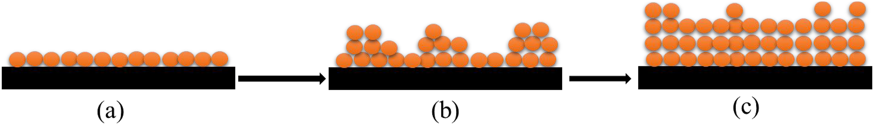
The mechanism of formation of the TiAlSi thin film coatings as explained by the Stranski-Kranstanov thin film growth theory, (a) Deposition of the wetting layer (Si + O2), (b) formation of 2D layers (TiAlSi), and (c) coalescence of the 2D layers to form 3D layers (TiAlSi).
Consequently, the deposition rate, which often determines the efficiency of the deposition process, was also observed to increase with an increase in the target power (Table 4), where the maximum deposition rate (0.151 nm/s) was obtained at the highest target power of 269.5 W. During sputtering of the TiAlSi thin films, the sputtering rate of the target (Vs) increased significantly with target power, as shown in Table 4. This deposition rate, according to Peter Sigmund's model of collisional sputtering, is dependent on the masses of the sputtering gas ions (Ar+) and target atoms and the surface binding energy of the target atoms. 24 Therefore, for the same target and other sputtering conditions, an increase in the target power increased the ion density in the deposition chamber, significantly increasing the deposition rate. 6
A topographical assessment of the surface of the TiAlSi thin films was conducted on the AFM scans using Gwyddion software (open source). The 3D and 2D scan images of the surfaces are given in Figure 4. The root mean square (RMS) roughness (Sq), the mean roughness (Sa), the maximum peak height (Sp), and the maximum pit depth (Sv) of the TiAlSi thin films deposited are presented in Figure 5.
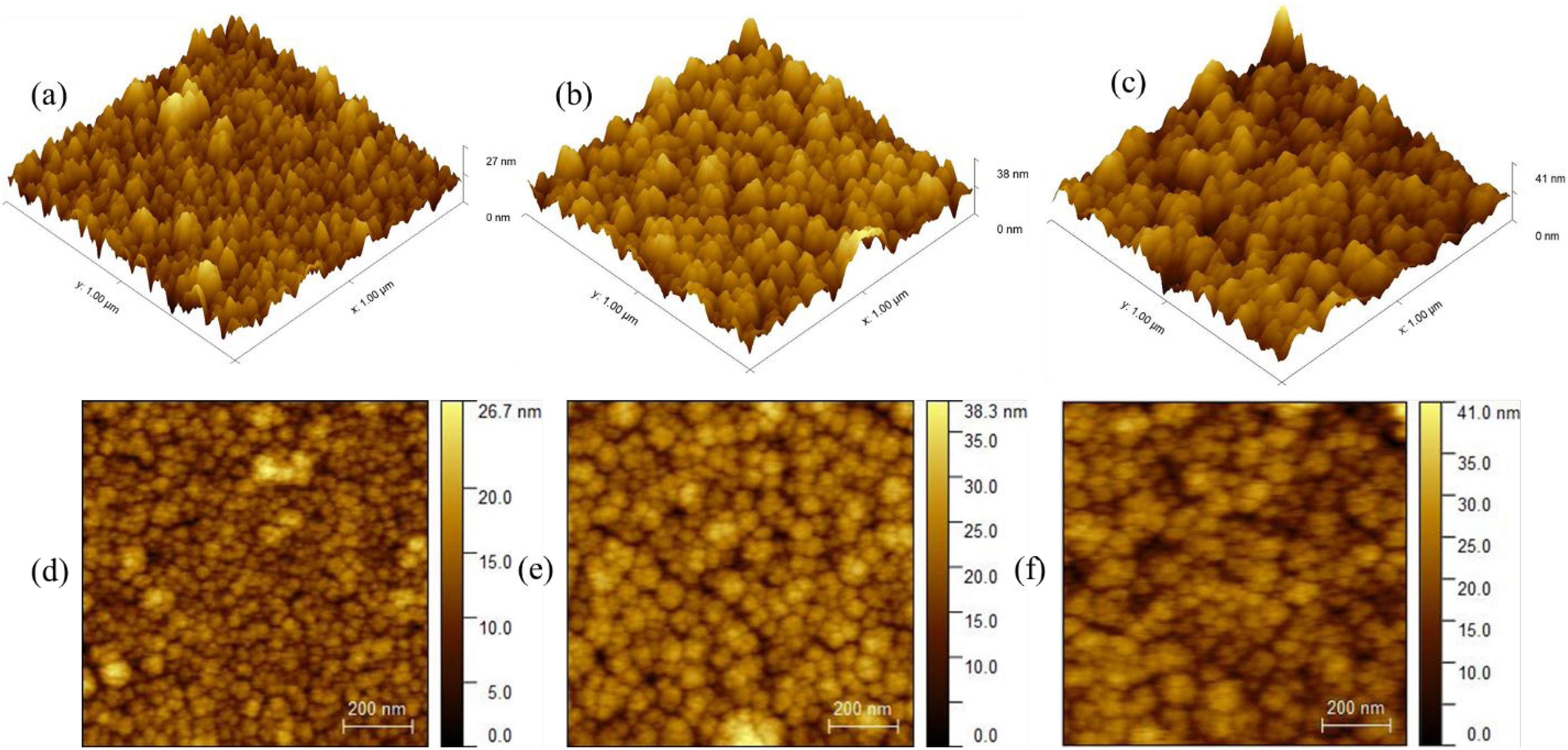
3D and 2D AFM images of tiAlSi thin films deposited at (a) and (d) 73.2 W, (b) and (e) 151.2 W, and (c) and (f) 269.5 W target power.
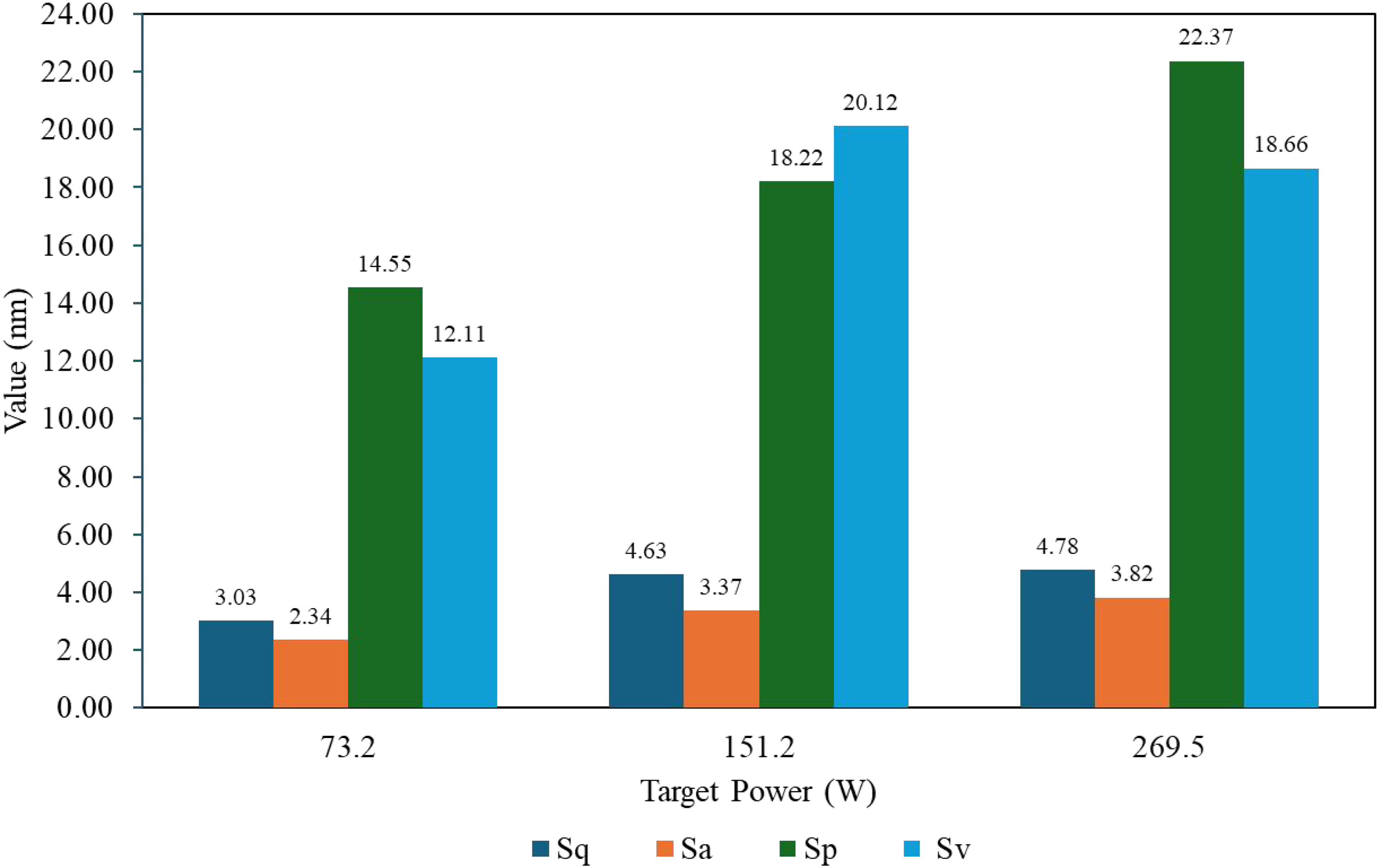
Sq, Sa, Sp, and Sv for the coatings deposited at different target powers.
An increase in the target power increased the roughness of the coatings deposited. A general trend was observed, with the lowest mean roughness (2.34 nm) obtained at the lowest target power of 73.2 W. An increase in target power increased the mean surface roughness to a maximum of 3.82 nm (at 269.5 W). This was consistent with the RMS roughness (Sq), which increased from 3.03 nm to 4.78 nm as the target power increased from P1 (73.2 W) to P3 (269.5 W), respectively. Further, the maximum peak height of the structures on the surface of the TiAlSi thin films increased (14.55–22.37 nm) with an increase in the target power (73.2–269.5 W). However, the maximum pit depth (Sv) increased from 12.11 nm (for 73.2 W) to 20.12 nm (for 151.2 W) but slightly reduced to 18.66 nm as the target power increased to the maximum (269.5 W).
Figure 6 shows the microstructure on the surfaces and cross-section of the TiAlSi thin films sputtered at different target powers. The average sizes of the surface structures were measured from the FE-SEM images using Fiji (open source software previously known as ImajeJ) in which an average of ten measurements of the lateral length of the structures was obtained as 43.4 nm (S.D = 3.0), 56.7 nm (S.D = 5.0 nm), and 75.4 nm (S.D = 9.0 nm) for the TiAlSi thin films deposited at 73.2 W, 151.2 W, and 269.5 W, respectively. Line profiles were also taken across the profiles of the AFM images to indicate the size, distribution, and peakiness of the surface structures and the roughness of the thin films. These line profiles with the position of acquisition (top right insert) are given in Figure 7. The topographical and microstructural analyses agreed, with both displaying an increase in the roughness of the TiAlSi coatings as well as an increase in the size of the surface structures, as shown by the AFM 2D images in Figure 4 (d, e, and f) and FE-SEM images in Figure 6 (a, b, and c). The average width of the structures (Figure 7) can be observed to significantly increase as the target power increases. This led to the formation of smooth-peaked, clustered, and fully-grown structures (Figure 6 (c)) compared to the small, sharp, and oriented structures of the thin film deposited at the lowest power (Figure 6 (a)).
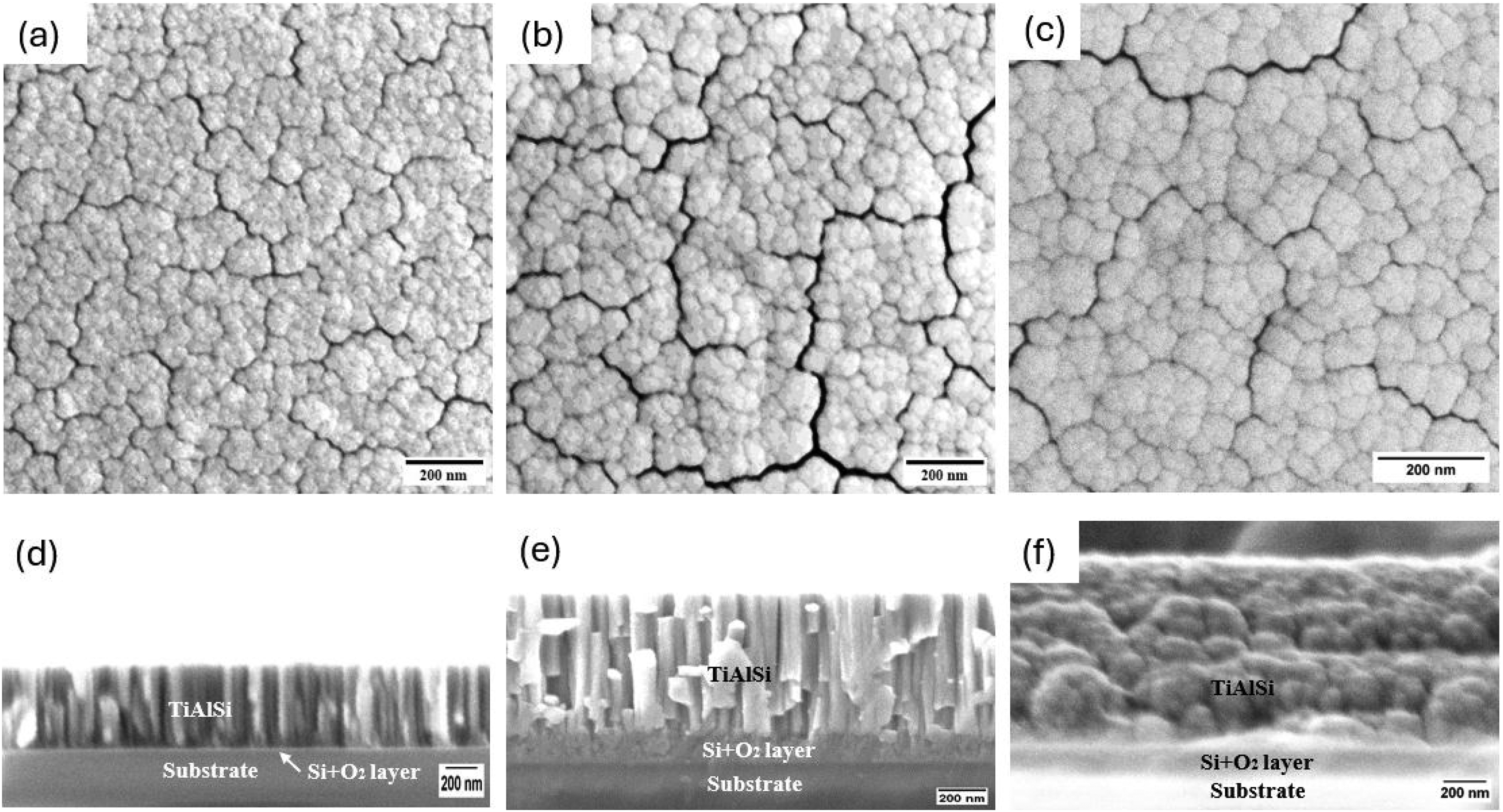
FE-SEM top-view and cross-section images of TiAlSi thin films deposited at (a) and (d) 73.2 W, (b) and (e) 151.2 W, and (c) and (f) 269.5 W target power.
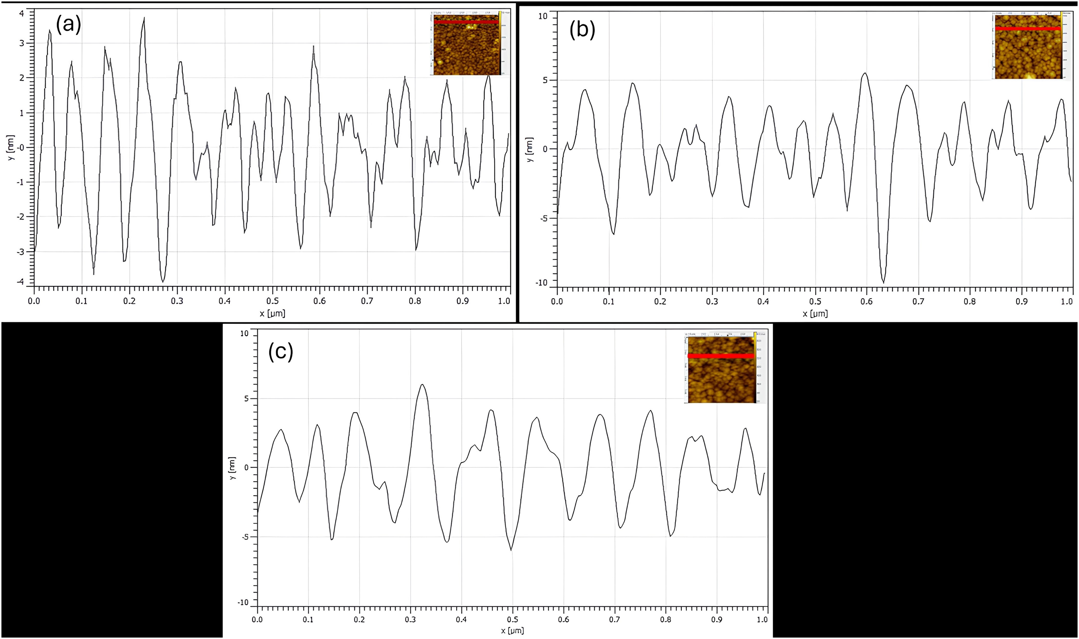
Line profiles of samples deposited at (a) 73.2 W, (b) 151.2 W, and (c) 269.5 W target power.
Further, there was an increase in the length and width of the surface cracks (boundaries) as the target power increased from 73.2 to 151.2 W. However, an increase in target power to the maximum (269.5 W) led to a slight reduction in the prevalence and length of the cracks (Figure 6 (c)). This explained why the maximum pit depth (Sv) of the TiAlSi thin films reduced as the target power increased from 151.2 W to 269.5 W as the cracks reduced. This can also be observed from the FE-SEM cross-sectional images of the TiAlSi thin films (Figure 6). As the target power increased from 73.2 to 151.2 W, the structure of the thin films changed from a columnar structure (Figure 6 (d)) to a grassy-cylinder-like structure ((Figure 6 (e)), and lastly to a solid packed cauliflower-like structure ((Figure 6 (f)). 3 This corroborates the increase in roughness values of the TiAlSi thin films as the deposition power increased. The sharp-peaked columns and grassy cylinders in samples P1 and P2 and the dome-shaped peaks in sample P3, which can be observed in the cross-section images, are also observed in the line scans (Figure 7).
As discussed earlier, an increase in the target power in the sputtering of TiAlSi thin films increased the plasma density, translating to an increase in the sputtering yield and inter-collision of sputtered adatoms in the chamber. This increased their mobility and deposition, hence increasing their surface diffusion. 3 This allowed the adatoms to self-align, which reduced the development of cracks, creating continuous, dense, and thick films with wide structures, as seen in Figure 6 (c) and (f) and Figure 7 (c). 25 Some of these wide structures observed on samples deposited at the highest power (269.5 W) were observed to grow into huge lumps of atoms because of the agglomeration of adatoms into 3-D islands. These fully grown ‘cauliflower-like’ shaped structures contributed largely to the unevenness of the thin film coatings deposited at high target power, which explained the high value of the maximum peak height of sample P3.26,27 An example of the ‘cauliflower’ shaped structures observed in high target power deposition of the TiAlSi thin films is shown in the FE-SEM image in Figure 8 (a) and a profile scan of the structure in Figure 8 (b). A measurement of the lateral diameter of the structure was approximately 578 nm.
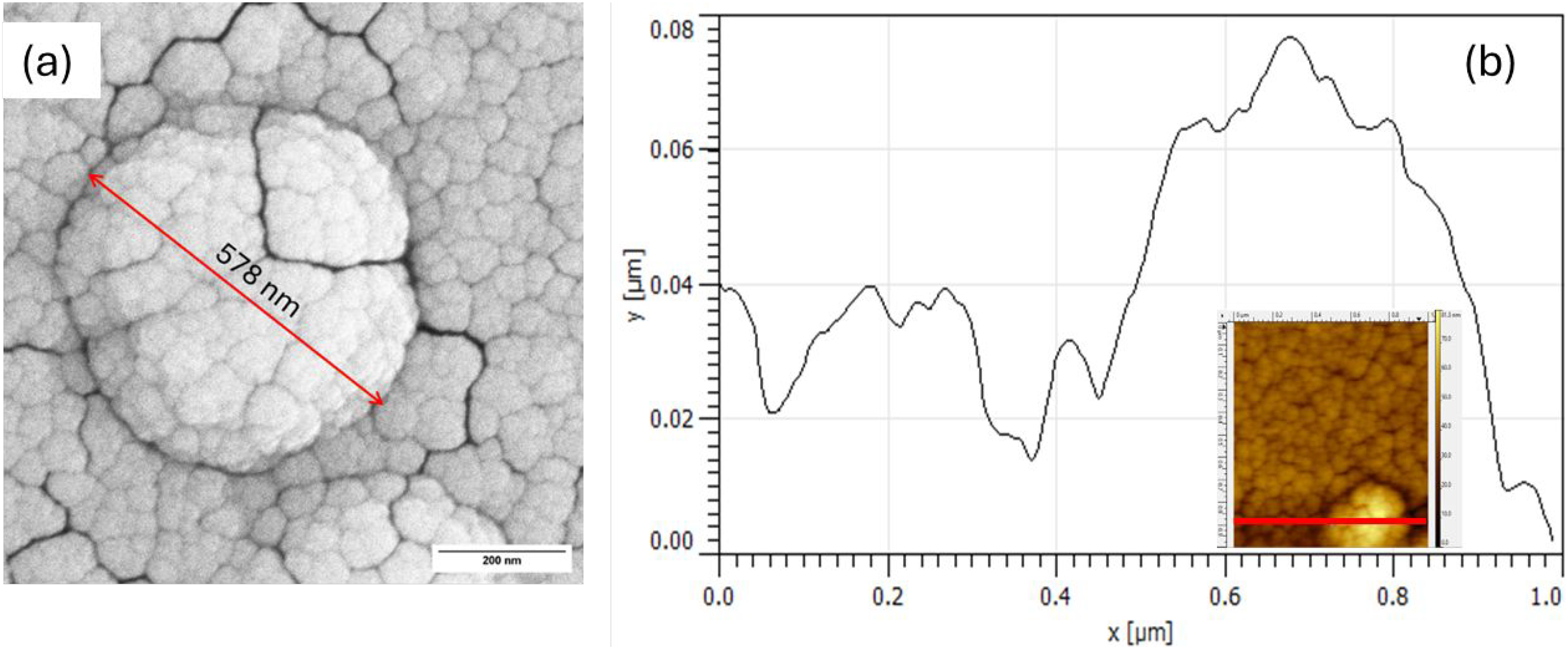
(a) FE-SEM and (b) profile plot of some surface structures formed in the sputtering of TiAlSi thin films at 269.5 W target power.
Lastly, an analysis of the crystal structure of the as-deposited TiAlSi thin films displayed the amorphous nature of the thin films deduced from the lack of observable X-ray diffraction peaks. However, broad humps were detected between 2θ = 20° and 2θ = 30° in all the thin films. These humps were related to the formation of the oxide of silicon, as reported in other studies.28,29 The diffractograms are shown in Figure 9.
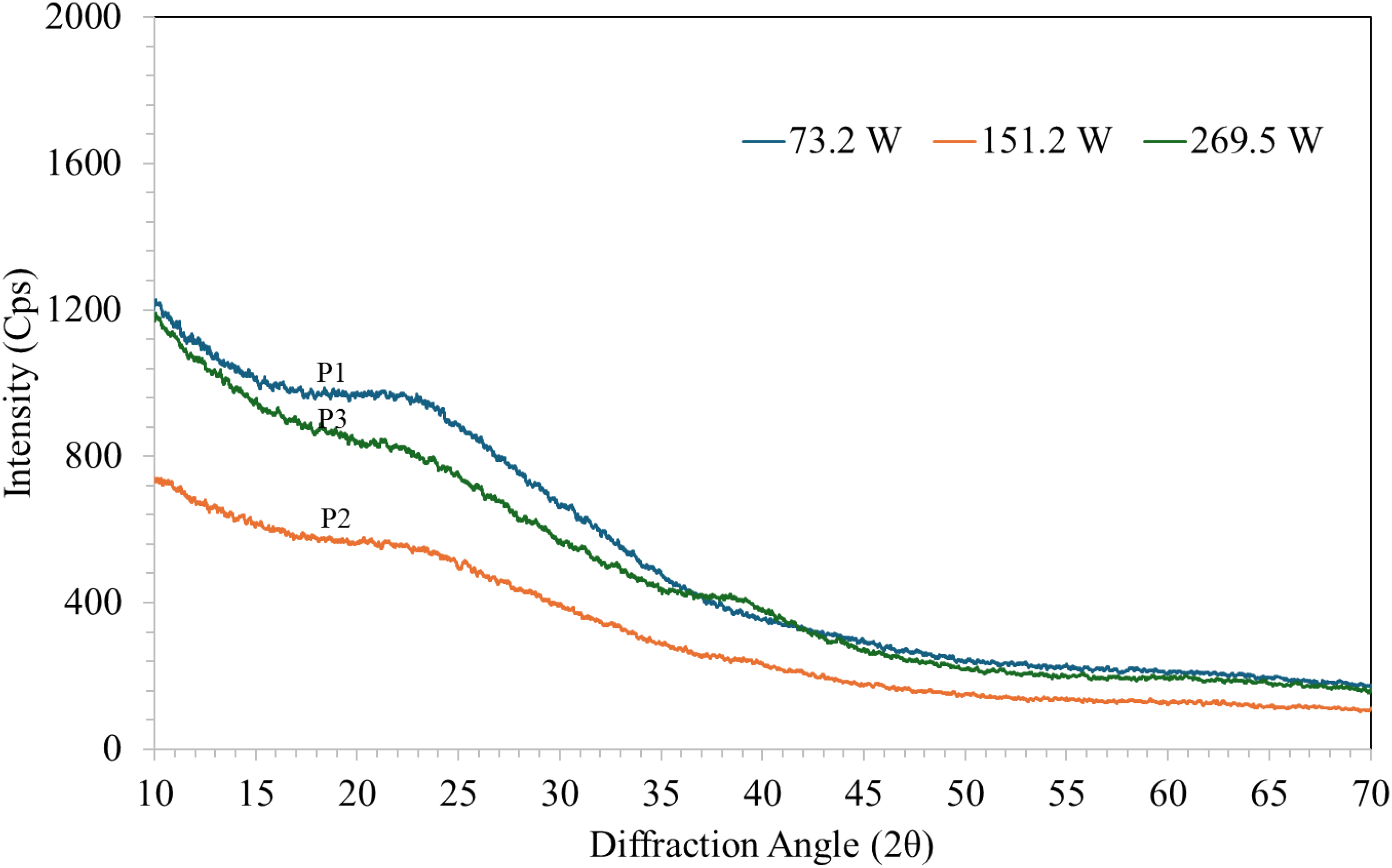
X-ray diffractograms of the as-deposited TiAlSi thin films.
Mechanical properties
The nano-hardness (H) and the reduced modulus (Er) were obtained from nano-indentation tests conducted and analysed according to the model proposed by Oliver and Pharr. 18 The loading-unloading curves are given in Figure 10.
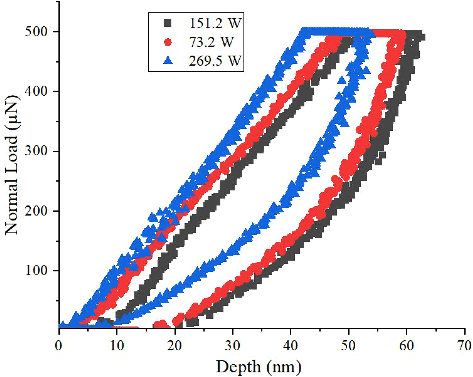
Load-displacement curves for the TiAlSi thin films deposited at varying target powers.
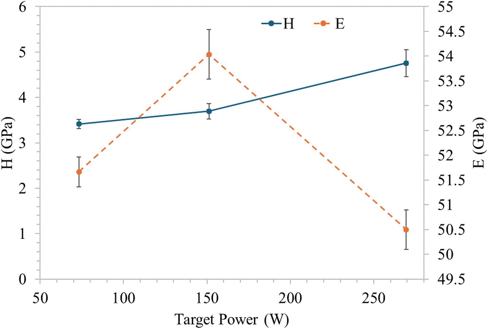
The Elastic modulus (E) of the TiAlSi thin films was computed from Er and plotted in Figure 11 together with the hardness of the thin films deposited at varying target powers. Similarly, the deformation factors, H/E and H3/E2, which show the elastic strain to failure and the resistance of the thin films to plastic deformation, 30 respectively, were computed and plotted in Figure 12.
Hardness (H) and Elastic Modulus (E) of the TiAlSi thin films deposited at 73.2 W, 151.2 W, and 269.5 W target powers.
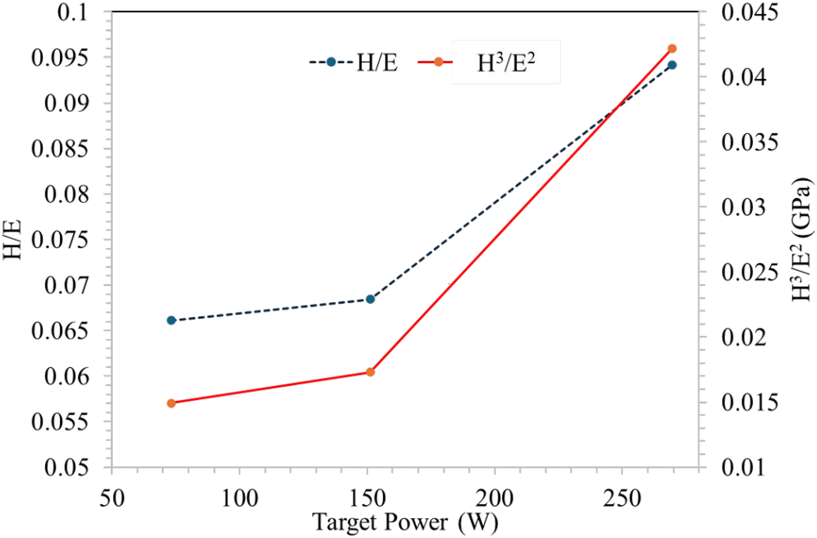
Ratios H/E and H3/E2 of the TiAlSi thin films deposited at 73.2 W, 151.2 W, and 269.5 W target powers.
An increase in the target power from 73.2 to 269.5 W was characterised by an increase in the hardness of the TiAlSi thin films from approximately 3.42 GPa (0.1 S. D) to 4.76 GPa (0.3 S. D), respectively, which represented approximately 39% increase. The change between films deposited at the lowest power (73.2 W) and the middle power (151.2 W) was small (∼ 0.28 GPa, ∼ 8%) compared to the significantly large change when the target power was increased to 269.5 W (∼ 1.06 GPa, ∼28%). This change was attributed to the significant increase in the density and continuity of the thin films and the reduction of the structure boundaries (Figure 6 (c) and (f)). On the other hand, the Elastic moduli (E) of the TiAlSi thin films increased from ∼ 52 GPa to ∼ 54 GPa for films deposited at 73.2 and 151.2 W target power, respectively, and then reduced significantly to ∼ 51 GPa. This depicted a reduction in the ability of the TiAlSi thin films deposited at high target powers to withstand elastic deformation. However, to further understand the plastic behaviour of the coatings, the plasticity index (H/E) and the plastic deformation factors (H3/E2) were obtained (Figure 12).
An increase in the target power (73.2–269.5 W) increased the plasticity index (H/E) from ∼ 0.066 to 0.094. This increase translated to an increase in the resistance of the TiAlSi thin films to abrasive wear and cracking as the target power increased. 31 Consequently, the plastic deformation factor (H3/E2) increased significantly from ∼ 0.015 to 0.042 GPa as the target power increased from 73.2 to 269.5 W, respectively. This factor represented the high resistance to plastic deformation of the TiAlSi thin films deposited at high target power, which can be linked to an increase in their fracture toughness. 30 An increase in the target power in magnetron sputtering increases the energy of the sputtered atoms, which not only align themselves on the surface but also undergo self-pinning and hardening as they bombard the already deposited atoms on the substrate. Moreover, densely packed surface structures in samples deposited at high power led to a reduction in the boundaries and mobility of the deposited atoms, which significantly reduced dislocation movements and increased the internal crystallinity, and hence the improvement in the mechanical properties of the TiAlSi thin films.2,32
Conclusions
In this study, for the first time, the influence of sputtering power on the growth of TiAlSi thin films from a composite target is reported. The following key conclusions can be drawn:
Upon sputtering of the composite target (Ti30Al16Si10 at. %) at target powers of 73.2 W, 151.2 W, and 269.5 W, uniform thin film alloys of Ti44.81Al16.17Si7.18, Ti46.56Al17.73Si7.70, and Ti47.13Al16.96Si7.50 at. %, respectively, were formed. For the first time, the work demonstrated the formation of a Si + O layer between the TiAlSi layer and the substrate. Further analysis will be necessary to understand its development and characteristics. With all the other deposition parameters kept constant, an increase in target power significantly increased the thickness, rate of deposition, and surface structure size of TiAlSi thin films. An increase in the target power significantly increased the roughness values of the TiAlSi thin films, with the maximum RMS roughness (4.78 nm) obtained at the maximum target power (269.5 W). All the coatings deposited at the varying target powers were amorphous. An increase in the target power improved the mechanical properties of the TiAlSi thin films, with an increase in the hardness, plasticity index, and plastic deformation factor of the films.
These findings show that during the sputtering process, precise control of the target power can produce stoichiometrically uniform TiAlSi thin films. Thin films produced at high target powers offer significant and attractive mechanical properties for use in the protection of surfaces in aggressive environments of high force, temperature, wear, and corrosion.
Footnotes
Declaration of conflicting interests
The authors declared no potential conflicts of interest with respect to the research, authorship, and/or publication of this article.
Funding
The authors received no financial support for the research, authorship, and/or publication of this article.