
Abstract
A locally resonant metastructure is a promising approach for low-frequency vibration attenuation, whereas the attachment of many resonators results in unnecessary and multiple resonance outside the bandgap. To address this issue, we propose a damping metastructure combining local resonators and an autonomous synchronized switch damping circuit. On the basis of modal analysis, we derive an electromechanically coupled equation of the proposed metastructure. The piezo ceramics, which are attached on a small portion of the metastructure and connected to the circuit, remarkably decrease the magnitude of the resonant vibration with no extra sensors, signal processors, or power sources. The displacement at unnecessary resonance was decreased by approximately 75%. The results of the coupled analysis were similar to the experimentally observed results in terms of the location and width of the bandgap on the frequency axis and the decreased displacement for the circuit. The proposed technique can overcome the disadvantage of the metastructure.
Introduction
A technique for reducing a mechanical vibration or noise in vehicles,1,2 aerospace structures, or industrial machinery 3 must satisfy the requirements of being lightweight, compact, low in power consumption, and cost-effective. A technique using a piezoelectric transducer 4 and the semi-active vibration attenuation termed as the synchronized switch damping on inductor (SSDI) 5 can satisfy these requirements, and its development is advancing. When the switch closes at the maximum/minimum of the piezo voltage, a high electrical current flows in the circuit and the piezo voltage flips immediately through the formation of an electrical connection between the inductor and piezo intrinsic capacitor. The vibrational energy of the structure is thereby dissipated. In an early phase of development, a signal processor and a sensor activated by an external power source were required to ensure the switch closes at the precise timing of the maximum/minimum of the piezo voltage. Subsequently, Lallart et al. 6 proposed a novel technique which allows to realize a self-sensing and self-powered system. Adopting the self-sensing and/or self-powered technique, derivative techniques such as a self-sensing (SS) synchronized switch damping on voltage (SS-SSDV) technique, 7 a SS-synchronized switch damping on negative capacitance (SS-SSDNC) technique, 8 and a SS-technique using a microcontroller unit with low power consumption9,10 were developed. These techniques can also be applied to reduce the level of sound induced by a structure’s vibration that is excited by a sound source. 11 Recently, to predict the attenuation performance of the autonomous SSDI technique more accurately, an electromechanical model incorporating nonlinear piezoelectricity was reported.12,13
A vibration attenuation technique of designing a metastructure is another promising approach. The metastructure is formed by deploying locally resonant structures periodically or creating a spatial variation in elasticity or mass density over a host structure. The metastructure can realize artificial properties such as negative mass and modulus, wave focusing and steering, elastic mirrors, or tunable bandgaps. 14 Based on the local resonance or Bragg scattering, the metastructure can form a shielding frequency band, which is referred to as a bandgap. Compared with the Bragg scattering metastructure, the locally resonant (LR) metastructure is more suited to attenuate low-frequency vibration, which occurs in vehicles1,2 or machinery 3 in the range of several tens to several hundreds of Hertz, because it allows the absorption of a vibrational wave whose wavelength is much larger than the lattice constant of the periodic structure. 15 The LR metastructure is formed by distributing mechanical or electromechanical resonators on a host structure periodically. This study briefly explains the state-of-the-art. To estimate the bandgap width of the LR beam, Liu et al. 16 proposed a transfer matrix method (TMM) and validated that the frequency response function obtained using the TMM was in good agreement with that obtained using the finite element method. To create multiple bandgaps and/or widen the bandgap, techniques using a four-link-mechanism, 17 interconnected resonator,18,19 or quadruple-mode resonator 20 were proposed. In the TMM, the Bloch’s theorem and/or the continuity between the neighboring unit cells are employed, whereas the vibrational mode shape function of the host structure, which is determined considering the boundaries, is not considered. For a metastructure, which has a finite number of resonators and is designed for attenuating low-frequency vibration, ignoring the mode shapes may lead to inaccurate prediction of the resonance frequencies or displacement outside the bandgap. Sugino et al.21,22 established an analytic methodology for the LR metastructure based on modal analysis and provided a closed-form solution for the bandgap width. Similarly, adopting the modal analysis, El-Borgi et al. 23 derived an equation of motion for the LR metastructure, allowing the creation of two bandgaps using two local resonators with different resonant frequencies. Unlike the aforementioned metastructure having a mechanical resonator, the metastructure having an electromechanical resonator uses piezo elements located periodically and a shunt circuit. Aghakhani et al. 24 developed a system-level analytic methodology for a plate-type piezo metastructure connecting to a resistive-inductive shunt circuit. Sugino et al. 25 proposed a methodology to achieve a wide bandgap by merging the bandgaps created by mechanical and electromechanical resonators. Chen et al. 26 realized an adaptive metamaterial beam by introducing a tunable electromechanical resonator, which comprises a piezo stack and shunt circuit with a negative capacitor and inductor. Compared with the use of the LR metastructure having a resistive-inductive shunt circuit, the use of the SSDI-based phononic metastructure reduces the required inductance remarkably, 27 allowing for a lightweight and compact metastructure. Bao et al. 28 proposed a unique technique of tri-interleaved SSDI topology, which uses the periodic cells of the piezo elements and the SSDI technique more efficiently. Based on the TMM, they derived a coupled equation of the complex system of the metastructure.
Given that piezo ceramics/stacks are costly, a large metastructure throughout which many of piezo ceramics/stacks are deployed24−28 may be impractical. This study considers a metastructure having mechanical resonators because of the cost-effectiveness and ease of design of such resonators. However, the addition of local resonators to the host structure creates unnecessary and multiple resonant peaks outside the bandgap. The resonant peaks on the low-frequency side pose a serious problem for practical application because the ambient vibration usually has a wide frequency band and the magnitude of displacement/acceleration at low frequency is large. 3 To address the practical problem, we propose a damping metastructure combining mechanical resonators and the autonomous SSDI technique. The piezo ceramics, which are attached on a small portion of the metastructure and connected to the circuit, decrease the magnitude of the unnecessary resonant vibration outside the bandgap with no requirement for any sensors, signal processors, or external power sources. It is important to develop an analysis technique for predicting the attenuation performance of the proposed metastructure. Two-way coupled analysis12,29,30 combining numerical software and a circuit simulator can precisely simulate electromechanical properties of the device using the synchronized switch technique, although the analysis requires a fair amount of computational time. In this paper, we establish a simpler numerical approach by simplifying the coupled equation. We employ a modal analysis approach to derive an electromechanically coupled equation of the proposed metastructure, considering a switching delay that cannot be negligible for the autonomous system. 31 We then solve the coupled equation and confirm that our modeling replicates experimental results.
Structure, circuit, and analysis
Metastructure
Figure 1 shows the damping metastructure embedded in the local resonators. Local resonators, each having a cantilever structure with a tip mass, were located periodically on the main composite beam with a spacing ls of 32 mm. As shown in Figure 1(b), a stainless-steel sheet (AISI304, thickness: 0.3 mm) with 12 side beams (27 × 10 × 0.3 mm3) was formed by electro-discharging machining. The metastructure was formed manually by inserting the thin stainless-steel sheet between two straight aluminum beams (AISI5052, 192 × 20 × 2 mm3 per beam, excluding the clamp part) and then attaching a steel mass (10 × 10 × 6 mm3) on the tip of the side beams and the piezo ceramics (Fuji Ceramics Corporation, Japan, C-6, 20 × 20 × 0.2 mm3 per sheet) on both sides of and near the edge of the composite beam. An epoxy structural adhesive (3M, DP460) was used to laminate the components. We attached a costly material of piezo ceramics on only a small portion of the metastructure, thereby realizing a cost-effective attenuation technique. We connected the two piezo ceramics in series to increase the electromechanical coupling and thus the damping force. The series-connected piezo capacitance Cp was 16.1 nF. The metastructure was designed to create a bandgap at the first eigenfrequency (approximately 86 Hz) of the composite beam with no local resonators. As explained later, the metastructure adversely has two resonant peaks near the edge of the bandgap. We decreased the displacement magnitude of the unnecessary resonant peaks using the piezo ceramics connected to the SSDI circuit. (a) Oblique view of the locally resonant metastructure with the piezo ceramics, (b) top view of the stainless-steel sheet, and (c) side and (d) front views of the metastructure.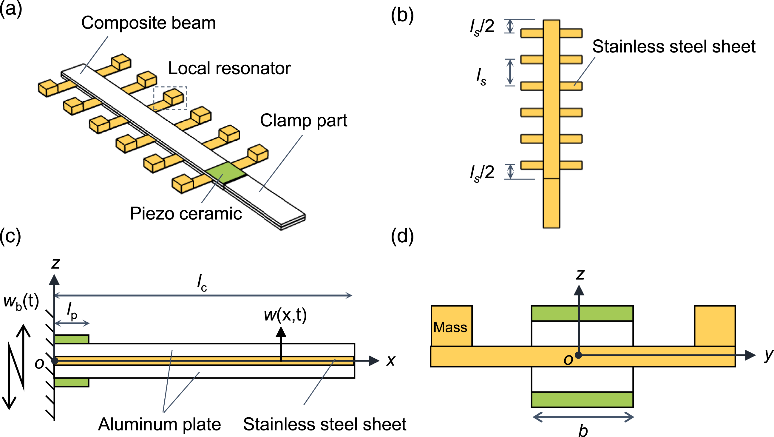
Autonomous SSDI circuit
Figure 2 shows schematics of the autonomous SSDI circuit used in this study and the waveforms of the piezo voltage vp and displacement in the steady state. The circuit topology was originally designed for the increase in the output voltage of vibration energy harvesters
32
; subsequently, it was applied to the SSDI technique.
12
The circuit in this study mainly comprises npn (Tr1 and Tr3, Nexperia, PBHV8140Z) and pnp (Tr2 and Tr4, Nexperia, PBHV9540Z) transistors, diodes (Diodes Incorporated, MUR120-T), a base resistor Rb (3.3 kΩ), an envelope capacitor Ced (1 nF), and an inductor L0. Compared with other SSD-based circuits,6−8 the circuit can increase the magnitude of the piezo voltage and thus the attenuation performance of the SSDI by decreasing Ced required. The advantage is greater for a device having series-connected piezo elements in which the envelope capacitance is not negligible compared with the piezo capacitance, because the circuit can reduce the electric current consumed in the envelope capacitor. As shown in Figure 2(b), when the positive switch closes for a period that is much shorter than the vibrational period of the metastructure, a high electrical current flows across the inductive circuit and vp flips immediately from vM to −vm. In the same manner, the negative switch activates with the opposite polarity of the current, voltage (from −vM to vm), and displacement. The parasitic resistor r in the inductive shunt circuit, which is the series resistance of the inductor, switch, and electrical wires, affects the inversion efficiency of the piezo voltage. The voltage ratio of vm/vM, which is referred to as the inversion coefficient γ, is a critical parameter that determines the attenuation performance. The piezo ceramics are open-circuited except for the switching. The autonomous SSDI circuit inherently causes a switch delay τ relative to the ideal switch timing because of the on-voltage threshold and the parasitic elements in the transistors and diodes.7,12 This study incorporates the switch delay into the model to replicate the real performance of the circuit. The detailed workflow of the circuit can be referred to in our previous paper
12
and a long explanation is omitted for brevity here. (a) Autonomous SSDI circuit and (b) waveforms of the piezo voltage vp and displacement in the steady state.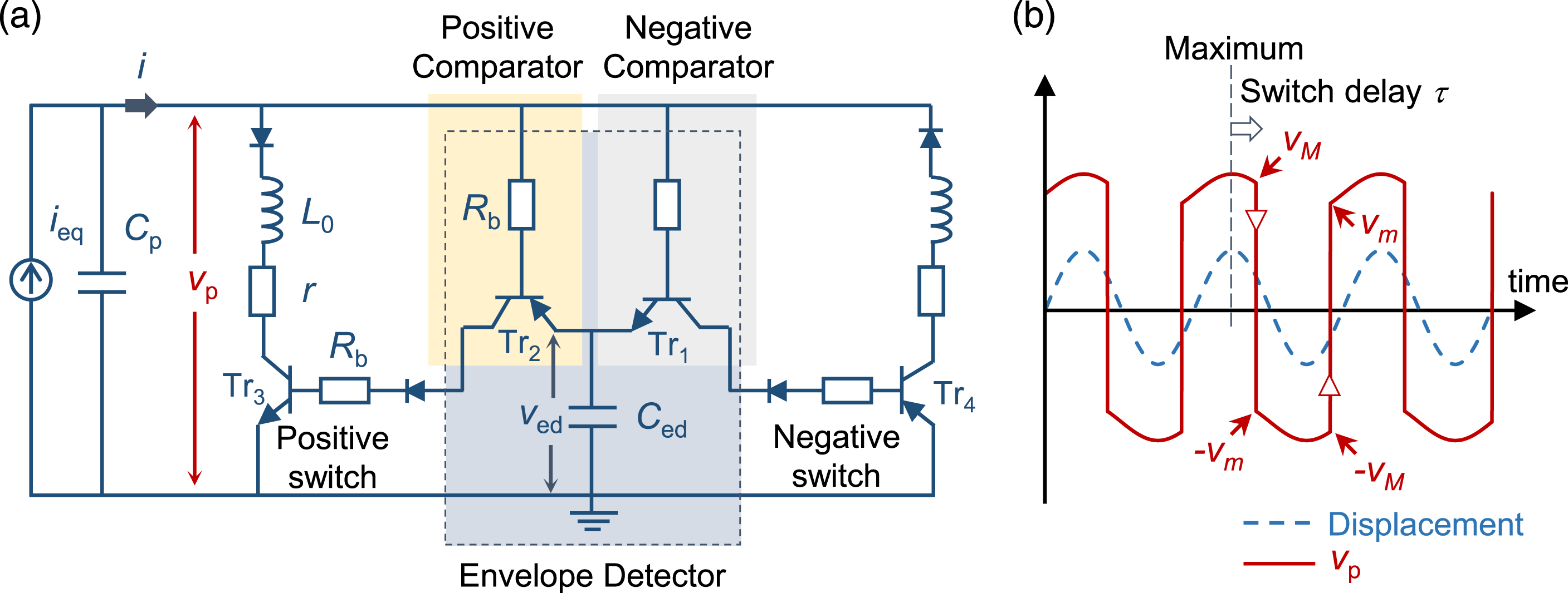
Coupled analysis
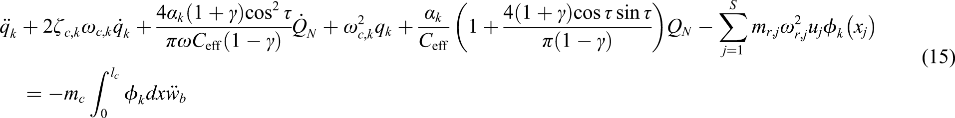
On the basis of modal analysis, we first derive a governing equation for the LR metastructure with the autonomous SSDI circuit and then solve the derived equation numerically.
31
As shown in Figure 1, the electromechanical equations for the proposed metastructure are derived as


We determine w(x,t) by solving the eigenvalue problem of the composite beam with no local resonators. Based on the discretization, w(x,t) can be expanded in series as


By substituting (4) into (5),


By substituting (4) into (1)−(3), multiplying by


We now determine the piezo voltage from the waveform shown in Figure 2(b). In general, the displacement or q
l
(t) can be expressed as a sine function of


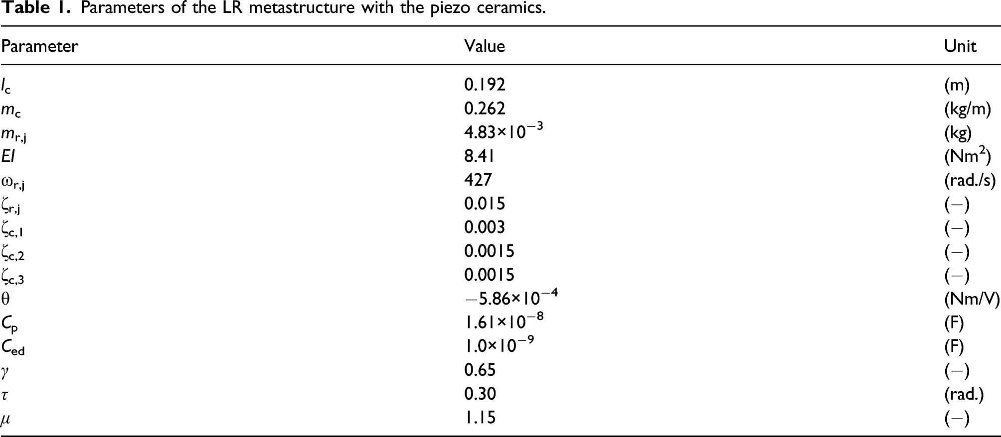
Parameters of the LR metastructure with the piezo ceramics.
We numerically investigate the transmissibility for the short and SSDI circuits to validate that the number of local resonators in this study is sufficient and the SSDI can decrease the peak magnitude of unnecessary resonance outside the bandgap. Figure 3 shows the transmissibility Tr for (a) the short-circuited and (b) SSDI circuit versus frequency and number of local resonators. When the piezo ceramics are short-circuited, the piezo ceramics act as a simple elastic material because vp and the piezo force become zero. Tr was obtained from wabs(xm,t)/wb(t), where xm is the location of the measurement of the displacement at a distance of 5 mm from the tip edge of the composite beam and wabs(xm,t) is the absolute displacement at xm. wb(t) was calculated as −a/(2πf),2 where a(t) and f are the acceleration and frequency, respectively. The magnitude of the acceleration was 0.2 G (1G = 9.8 m/s2) from 20 to 65 Hz, 2G from 70 to 95 Hz, and 1G from 100 to 180 Hz to match the experimental condition explained in the next section. For reference, the broken lines indicate the bandgap edges, which were estimated analytically based on the previous study.
21
The estimated bandgap ranges from Transmissibility Tr for (a) the short-circuited and (b) synchronized switch damping on inductor circuits versus frequency and number of local resonators. The broken lines indicate the estimated bandgap edges.
21
The mass ratio μ of the local resonators to the composite beam is held constant in the numerical analysis.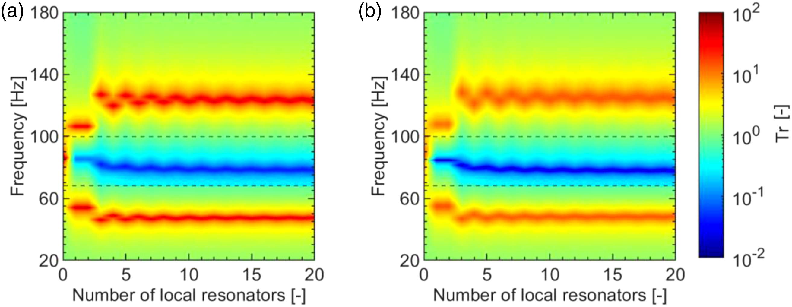
Results and Discussion
We now investigate how the magnitude of the displacement can be decreased using the small piezo ceramics connecting to the SSDI circuit, both numerically and experimentally. We compare results for the short-circuited (SC) and autonomous SSDI circuits. Figure 4 shows the equipment for measuring the absolute displacement wabs and piezo voltage vp of the metastructure. A shaker applied a sinusoidal vibration by setting a frequency and acceleration. A laser displacement sensor (LK-H150, LK-G5000, Keyence) was used to measure the displacement. The signals of the displacement, piezo voltage, and acceleration were collected via an oscilloscope and analyzed on a personal computer. wabs was measured at a distance of 5 mm from the tip edge of the composite beam. The transmissibility Tr was obtained from the absolute value of wabs/wb, where wb is the base displacement applied by the shaker. wb can be calculated as −a/(2πf)2, where a and f are the acceleration and frequency applied by the shaker, respectively. Similar to the experiment, Tr in the numerical analysis was obtained from wabs(xm,t)/wb(t), where xm is the location of the measurement of the displacement. The attenuation efficiency was calculated as 20log10(wabs, SSDI/wabs,SC), where wabs, SSDI and wabs,SC represent the displacement for the SSDI and short circuits, respectively. This study applied a different magnitude of the acceleration depending on the frequency, because the displacement magnitudes at the first and second resonances were greatly different at the same acceleration level and a sufficiently large signal of wb was required to estimate the bandgap precisely, compared with the ground electrical noise. As shown in Figure 5, pulsebeat wave was observed at the first resonance when the impulsive damping force induced by the SSDI circuit was excessively strong. A different inductance was employed for the first (47 mH) and second (1 mH) resonances to avoid the complexity observed in the waveform. Equipment for evaluating the attenuation performance. PC: personal computer, SSDI: synchronized switch damping on inductor, USB: Universal Serial Bus. Pulsebeat wave induced by a strong impulsive force of the SSDI circuit at the first resonance.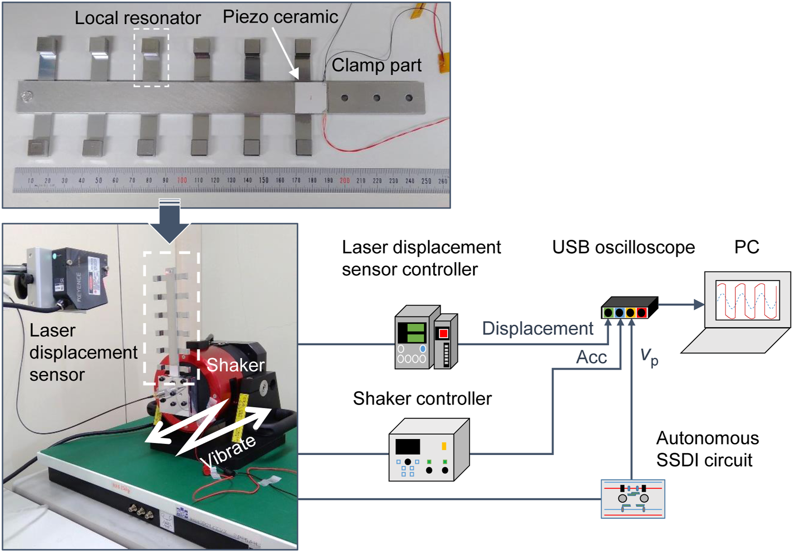
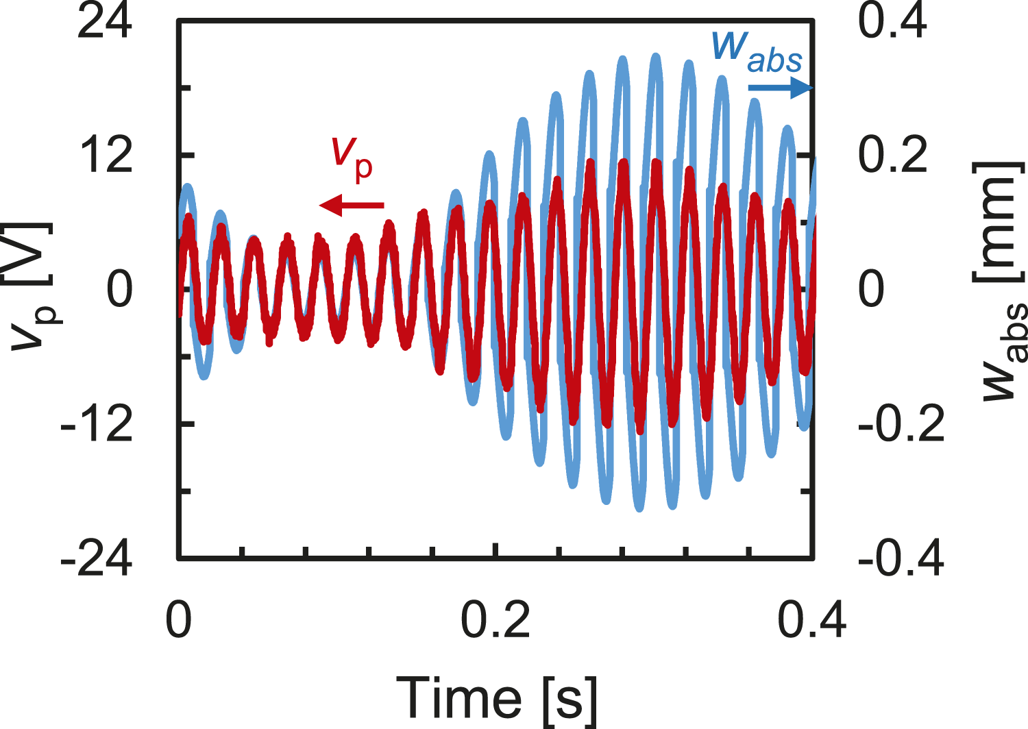
Figure 6 shows the experimental and simulation results of transmissibility Tr and the frequency response curves of the displacement wabs for the SC and SSDI circuits around the first and second resonances. The solid lines and circles respectively represent the simulation and experimental results. For reference, the estimated bandgap edges discussed in the subsection of Coupled analysis were shown in Figure 6(a) as broken lines. The magnitude of the applied acceleration was 0.2 G (1G = 9.8 m/s2) from 25 to 65 Hz, 2G from 70 to 95 Hz, and 1G from 100 to 180 Hz. The resonance frequency fr and displacement wabs at the first and second peaks were listed in Table 2. The relative error was calculated as |Simulation−Experiment|/Experiment. Overall, the numerical analysis showed a behavior similar to that of the experimentally observed results and replicated the location and width of the bandgap on the frequency axis and the decreased displacement for the SSDI circuit. There was a difference in the bandgap depth of the transmissibility between the experiment and simulation, because non-negligible noise remained in the displacement and acceleration signals, and a design error of the local resonators may cause a noise vibration. As shown in Figure 6(a), the bandgap formed from 73 to 100 Hz in the experiment and from 68 to 100 Hz in the simulation, when the bandgap is defined as Tr < 1. As shown in Figure 6(a), the SSDI circuit did not affect the characteristics of the bandgap because a small displacement in the bandgap cannot apply sufficiently large stress to the piezo ceramics. As shown in Figure 6(b) and (c), the piezo ceramics connected to the SSDI circuit markedly reduced the first and second resonant vibrations outside the bandgap. The attenuation efficiency at the first resonance was −11.8 dB for the experiment and −11.1 dB for the simulation, and the attenuation efficiency at the second resonance was −13.4 dB for the experiment and −11.1 dB for the simulation. The displacement for unnecessary resonance outside the bandgap thus decreased by approximately 75%. Experimental and simulation results of (a) transmissibility Tr and the frequency response curves of the displacement wabs for the short-circuited (SC) and synchronized switch damping on inductor (SSDI) circuits around (b) the first and (c) second resonances. The broken lines indicate the estimated bandgap edges.
21
. The resonance frequency fr and displacement wabs at the first and second peaks.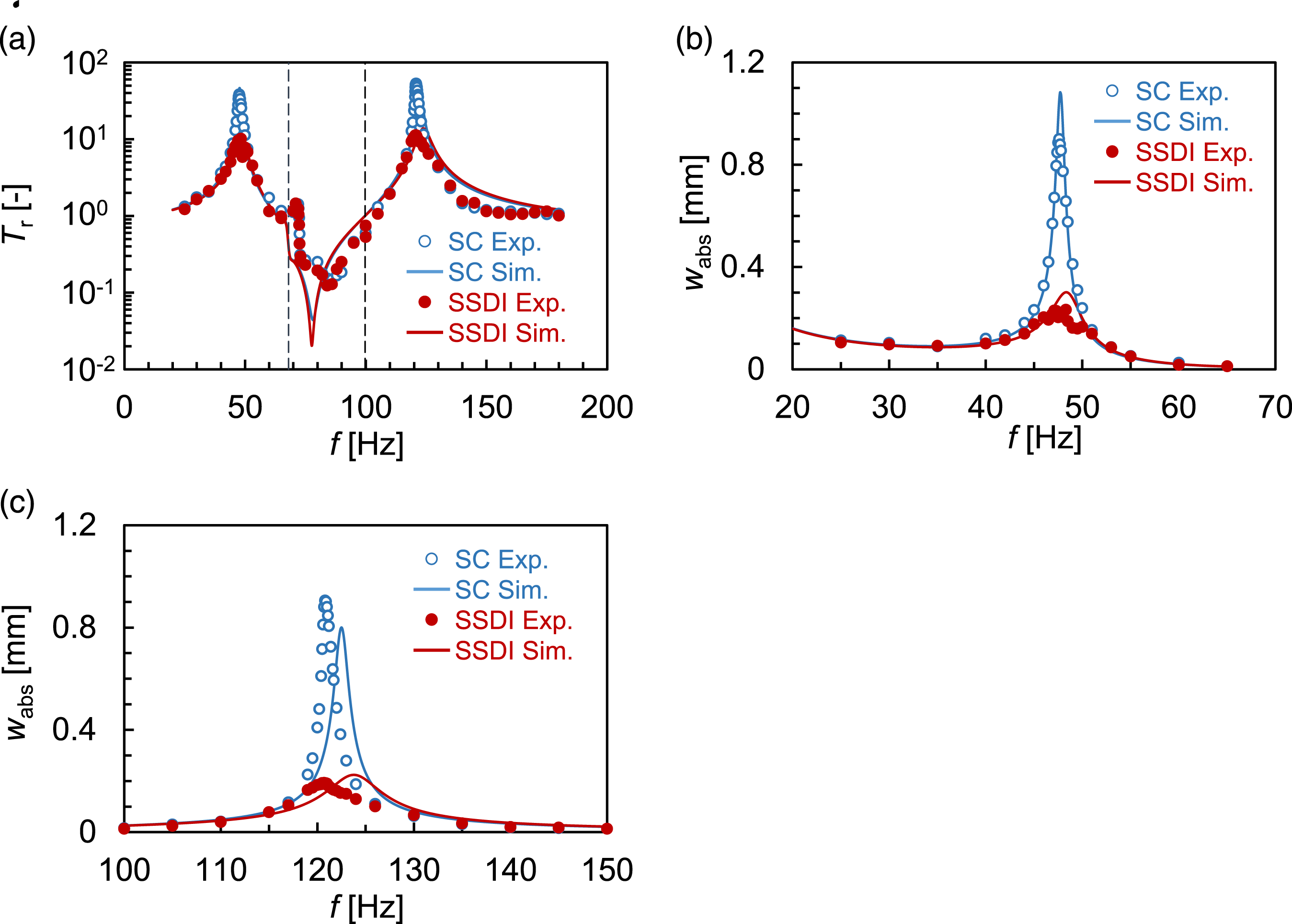
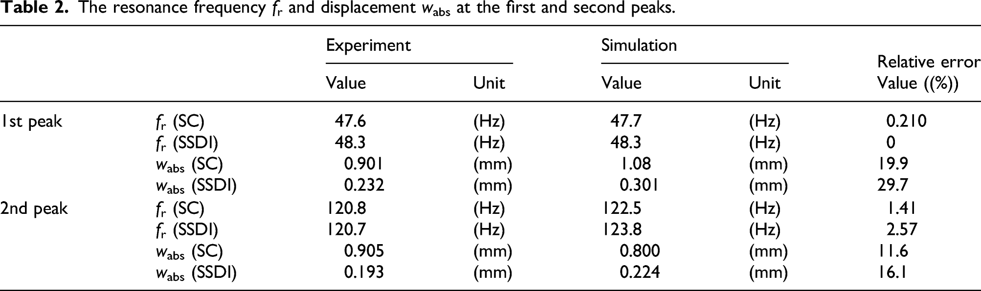
Figure 7 shows the experimental results of waveforms of the displacement wabs and piezo voltage vp at the first and second resonances. As explained in the subsection of Autonomous SSDI circuit, the SSDI circuit flipped the piezo voltage at a little over the maximum/minimum displacement. The switch delay was clearly observed in the waveform. This study incorporated the non-negligible parameter in modeling and the simulation thus replicated the attenuation performance well. Waveforms of the displacement wabs and piezo voltage vp at the (a) first and (b) second resonances.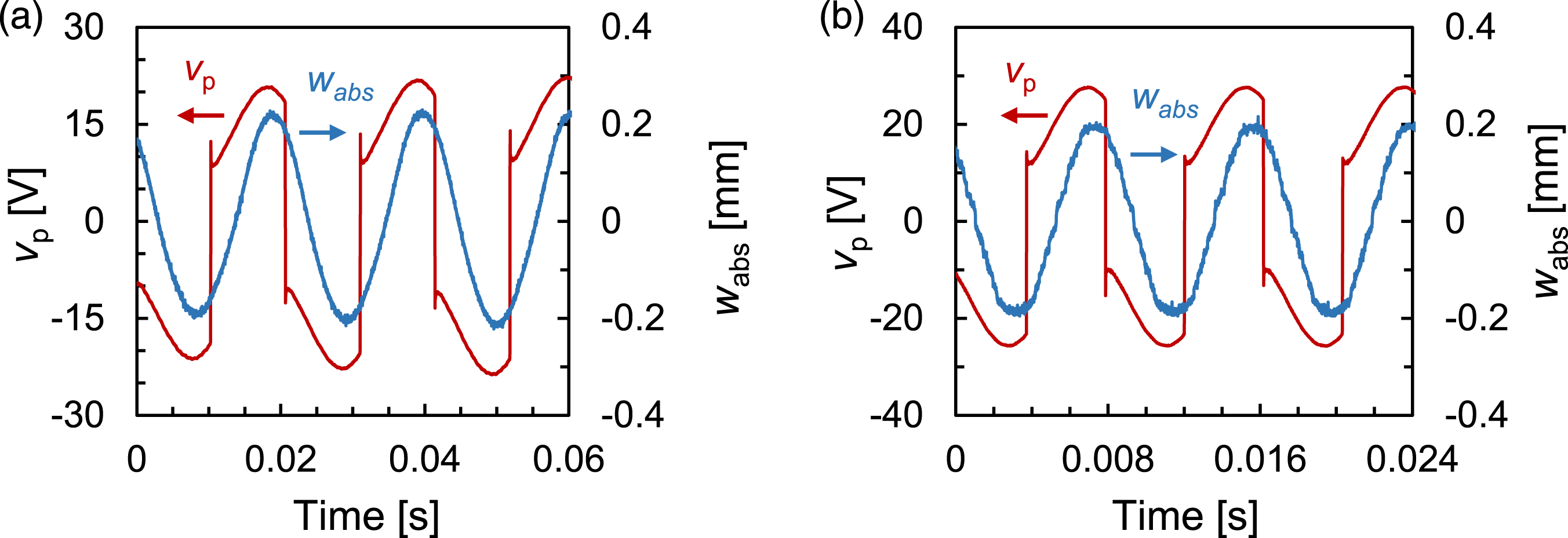
To investigate the potential of the proposed technique in a simple manner, this study used a linear model of the piezoelectricity and damping in modeling. However, similar to the case of previous studies,12,13 the nonlinear piezoelectricity and damping may need to be included in modeling to predict the frequency response of the displacement and damping performance more accurately. At the second resonance, an 1.4% difference in the short-circuited resonance frequency between the experiment and simulation was observed, which may be attributed to the softening effect of the nonlinear piezoelectricity. Our future work will focus on establishing a more precise model for the LR metastructure with the autonomous SSDI circuit, considering the material and damping nonlinearities.
Owing to the sufficiently large piezo voltage, the autonomous SSDI technique in this study decreased the displacement by approximately 75%. For high frequencies beyond several kHz, the proposed technique may not work because the stress/strain imposed to the piezo material and thus the piezo voltage would be too small to activate the autonomous SSDI circuit. Re-designing the thickness ratio of piezo materials to substrate and using a microhenry inductor may be possible approach for the high frequency application. In this study, the coupled equation (15) was derived, assuming that the switch closes at every maximum/minimum displacement. For a random vibration, a switch-skipping 29 will occur when a sufficiently large piezo voltage is not available. Our future work will also focus on including the switch-skipping in modelling.
Conclusion
A locally resonant metastructure can attenuate low-frequency vibration by forming a bandgap, whereas the attachment of many mechanical resonators throughout the host structure leads to unnecessary and multiple resonance outside the bandgap. To address the practical issue, this study proposed a damping metastructure combining local resonators and an autonomous synchronized switch damping circuit. The piezo ceramics, which are attached on a small portion of the metastructure and connected to the autonomous SSDI circuit, can reduce the resonant vibration with no extra sensors, signal processors, or power sources. Thus, the combinational technique achieves both high attenuation performance and cost-effectiveness. This study employed the modal analysis approach and derived an electromechanical equation for the proposed metastructure, considering a non-negligible switch delay. Overall, the numerical analysis showed a behavior similar to that of the experimentally observed results and replicated the location and width of the bandgap in the frequency axis and the decreased displacement for the SSDI circuit. The use of the SSDI circuit decreased the displacement for unnecessary resonance outside the bandgap by approximately 75%.
Footnotes
Declaration of conflicting interests
The author(s) declared no potential conflicts of interest with respect to the research, authorship, and/or publication of this article.
Funding
The author(s) disclosed receipt of the following financial support for the research, authorship, and/or publication of this article: The authors received financial support from the JKA Foundation and its promotion funds from KEIRIN RACE.