
Abstract
We observed a linear behaviour of intermetallic compound (IMC) layer growth in electronic metallurgical interconnections, although the time required was twice that of commercial reliability standards for electronic packaging. This finding contradicts the classical parabolic growth law, which is widely reported to represent growth behaviour. We suggest that the parabolic growth law may be inadequate to thoroughly explain the IMC layer's growth by considering (a) one-directional growth and (b) reactions between elements for formation and growth. Further analysis has been carried out to analyse the logical judgment of the parabolic growth law and support our finding over linear IMC layer growth behavior.
Keywords
Introduction
Intermetallic compound (IMC) layer growth in electronic metallurgical interconnection joining has attracted considerable interest in the past decades. The IMC layer is essential for joining purposes because it provides good metallurgical bonding in electronic devices. Good interconnection in electronic devices is crucial for structural integrity and electrical connection. The growth of the IMC layer is being assessed due to its relationship to the reliability of the solder joint. The stability of the IMC layer growth within certain periods and service conditions gave rise to the structural integrity and reliability of the solder joint and impacted the lifespan of the electronic products. Excessive growth of the IMC layer is a major issue in the metallurgical solder joint, which contributes to its detrimental effect on solder joints because of its brittle nature. Thus, understanding the IMC layer growth behaviour subjected to reliability testing is extremely important in evaluating the solder joint's structural integrity, stability, and reliability.1–3
Numerous studies have been conducted on the growth of the IMC layer subjected to reliability testing in terms of its formation, growth behaviour, size, shape, and relationship with the mechanical reliability and lifespan of electronic devices.4–10 For instance, a recent study by Zarmai et al. 11 highlighted the relationship between the IMC layer thickness and the thermomechanical reliability of solder joints. Higher IMC layer thickness has decreased the solder joint fatigue life. Tian et al. 12 reported that cracks were formed between the solder interface and IMC layer after 250 cycles of thermal shock. These cracks occurred because of the different coefficients of thermal expansion of the Sn-3Ag-0.5Cu solder and IMC layer and the increasing thickness of the IMC layer. This agrees with the findings reported by Zhu et al., 13 who observed that the thickening of the IMC layer boosts crack propagation and weakens joint strength. Regarding the microstructural evolution in the IMC layer, Sayyadi et al. 14 examined the morphology of IMC layers and found that the structure changed from a scallop-like shape into a planar shape due to isothermal aging. An and Qin 15 observed that cracks tend to occur in thick IMC layers with planar microstructures. Hu et al. 16 reported similar observations, stating that cracks occurred at the solders in thick IMC layers owing to the inherent brittleness of the IMC layers.
In assessing the IMC layer growth, it is generally accepted that the IMC layer growth behaviour followed the parabolic growth law given by:


Growth exponent and claimed growth behaviour of IMC layer subjected to isothermal ageing.
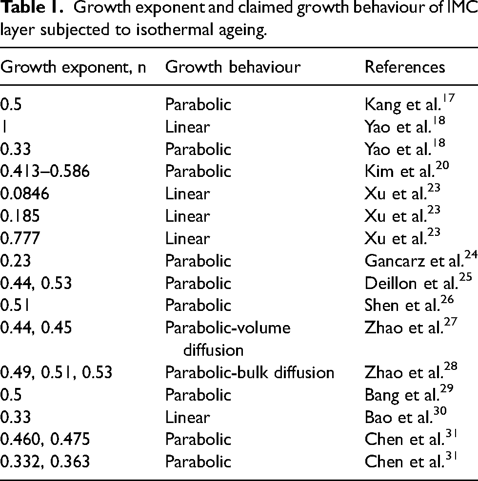
Table 1 presents the calculated growth exponents and claimed growth behaviour for IMC layer growth reported by different researchers. From Table 1, the claimed growth behaviour of IMC layer growth is parabolic, while the growth exponent n is reaching a value of 1, which implies linear growth behaviour. Furthermore, Xu et al.
23
claimed the IMC layer growth follows a linear relationship. But, by taking a closer look at their analysis, they are assuming the IMC layer growth is adopting the parabolic growth law
To understand the growth behaviour, from the theoretical aspect of grain growth, a few basic models are considered for analysing the IMC layer growth, including the one proposed by Burke and Turnbull,
32
Smith,
33
and Hillert et al.
34
The classic model developed by Burke and Turnbull for grain growth is useful for understanding the parabolic growth law associated with IMC layer growth. The growth theory is based on boundary migration under pressure due to surface curvature. The relationship is expressed as follows:


Smith 33 discusses the growth mechanism in terms of grain growth topology in terms of space filling and surface tension. A hexagonal 2D grain that consists of six sides is stable with side angles of 120°. 35 A grain with less than six sides will shrink, while a grain with more than six sides tends to grow. 35 Further, Hillert et al. 34 proposed a growth theory based on dislocation climb. According to their deduced parabolic growth kinetics, the rate of grain growth depended on the number of defects per grain, and these defects caused grain shrinkage. The climbing of cellular dislocations was associated with grain growth, which involved topological step changes from cell annihilation to face annihilation to neighbour switching.
The theories proposed by Smith and Hillert can explain grain growth, but they consider only the overall growth of grains from many individual grains. However, IMC layer growth does not involve many individual grains but exists as a single phase. Furthermore, IMC layers do not require grains to accommodate themselves, in contrast to normal grain accommodation in the polycrystal growth process. In addition, if IMC layer growth is not in line with the assumptions proposed by Burke and Turnbull, then the fundamental growth mechanism and behaviour of IMC layers must be considered.
Realizing the gap in previous research on the consideration of using the parabolic growth law to represent the growth of the IMC layer, this work is aimed at investigating the growth behaviour of the IMC layer for solder joints subjected to reliability testing and isothermal aging at 150°C beyond the standard duration (1000 h) up to 2000 h. This work emphasized the need to reassess the claimed growth theory commonly used for analysing IMC layer growth adopted in electronic metallurgical interconnections, that is, the parabolic growth law. This work also advocates that the following factors must be considered before directly choosing the parabolic growth law to evaluate and represent the IMC layer's growth behaviour due to thermally activated processes:
Growth is going in one direction as the IMC layers are growing towards the solder area only. IMC layer formation occurs due to reactions to form compounds or phases from different species, such as Sn and Cu in Sn-based solders and Cu substrate systems.
Materials and method
A lead-free solder joint has been used to investigate metallurgical interconnections that consist of Cu substrate on the printed circuit board (PCB) and a lead-free solder alloy. Lead-free solder paste, Sn-0.3Ag-0.7Cu (SAC 0307), with type 4, consists of solder alloy particles ranging from 20 to 38 µm. The solder paste was then printed on the Cu pads of the PCB via stencil printing. The printed PCB was then reflowed in the reflow oven for the soldering process to establish the solder joint.38,39 The samples were then subjected to annealing during high-temperature storage (HTS) testing in an oven at 150°C for 200, 400, 600, 800, 1000, 1200, 1400, 1600, 1800, and 2000 h to facilitate IMC layer growth. Each sample was taken out of the oven at every interval HTS time and prepared for cross-section via standard metallographic technique, involving the cutting process, grinding process, and polishing process.40,41 The samples were cut using a sawing machine (Buehler, Isomet 1000), cold mounted in a mixture of epoxy resin and hardener, grounded (PM-1V) with SiC abrasive paper from 800, 1000, 1200, 2000, and 4000 grit with a speed of 50–100 rpm, and polished (PM-1V) using Dp-Nap polishing cloth and diamond sprays of 6 and 1 µm with a speed of 50 rpm. The microstructure of the solder joint, which consists of Cu substrate, IMC layer, and solder matrix, was observed and analysed qualitatively and quantitatively using focus variation microscopy (Alicona, G4)38,42 and a field emission scanning electron microscope equipped with energy dispersive spectroscopy (ZEISS, MERLIN COMPACT) for morphology and elemental characterisation. The average IMC layer thickness has been estimated from 300 measurement points for each HTS time. To analyze the behaviour of the IMC layer growth model, a mathematical expression based on the shape of parabolic growth from a layer is analysed.
Results and discussions
Figure 1 shows the plot of the IMC layer thickness versus the annealing time during the HTS test, indicating the growth behaviour of the IMC layer. This figure shows a linear relationship exists between the IMC layer thickness and HTS time up to 2000 h. From an industrial viewpoint, the HTS test is widely used to evaluate the reliability of solder joints according to the JESD22-A103D standard up to 1000 h. 43 Apparently, most of the previous studies on IMC layer growth followed the parabolic growth law without clear evidence or understanding of the basis for using it. For instance, several researchers used the parabolic growth law (n = 0.517, n = 0.517,20,44,45 without determining the growth exponent. On the other hand, there are also claims that IMC growth can follow a linear or parabolic path. 20,44,46 This shows that the understanding of the IMC's growth behaviour is still unclear. A detailed analysis of Figure 1 indicates that the growth exponent, n = 1, is due to the linear relationship between the IMC layer thickness and high temperature storage time. This shows a deviation from the parabolic growth law. Therefore, we suggest that the growth of the IMC layer does not fit with the parabolic growth law (at least up to a certain time, up to 2000 h in this case) and propose certain considerations for assessing the growth behaviour of IMC layers.
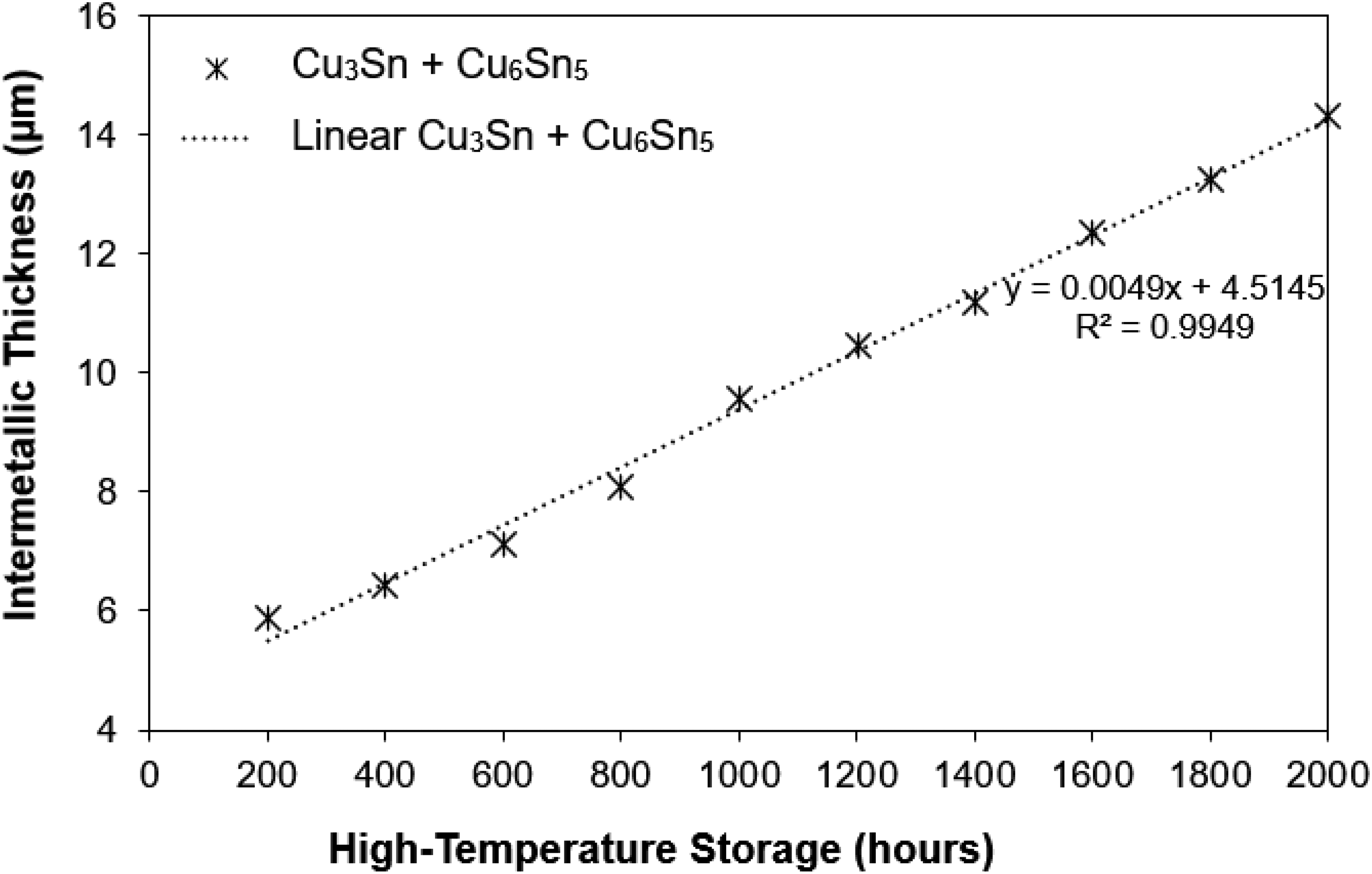
IMC layer growth was determined using SAC 0307 on PCB/Cu during HTS test at 150°C up to 2000 h.
Figure 2 shows FESEM micrographs and EDX mapping of the SAC 0307 solder joint after the HTS test at 150°C for 1000 h. It is observed that the IMC layer has been formed between the Cu substrate and the solder alloy. The formation and growth of the IMC layer occur through the reaction between Sn and Cu.
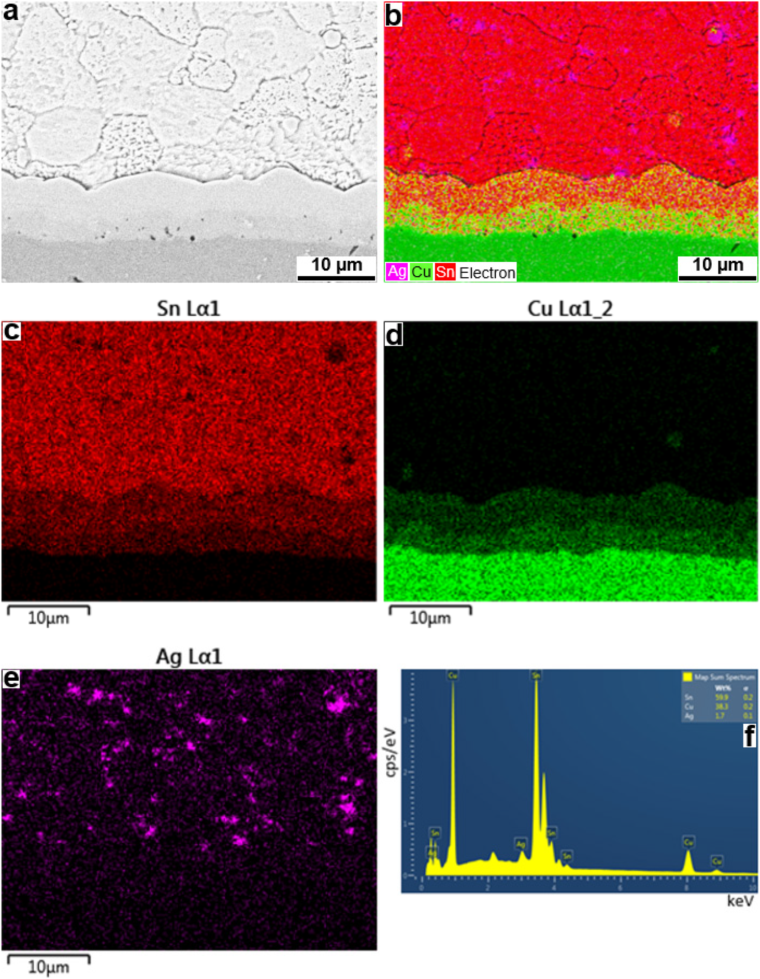
Micrograph of SAC 0307 solder joint after HTS test at 150°C for 1000 h: (a) FESEM micrograph, (b) EDX mapping area of (a), (c) EDX mapping of Sn element, (d) EDX mapping of Cu element, (e) EDX mapping of Ag element and (f) EDX spectrum of mapping area (a).
It is also observed that the growth of the IMC layer is towards the solder matrix, which is only in one-directional (ID) growth. The Cu substrate did not show any direction of IMC growth. The IMC layer observed exists along the solder joint between the Cu substrate and the solder area coverage. The growth of the IMC layer was also limited at the edge of the solder joint.
To further clarify the shape of the growth layer, we consider a parabolic on the
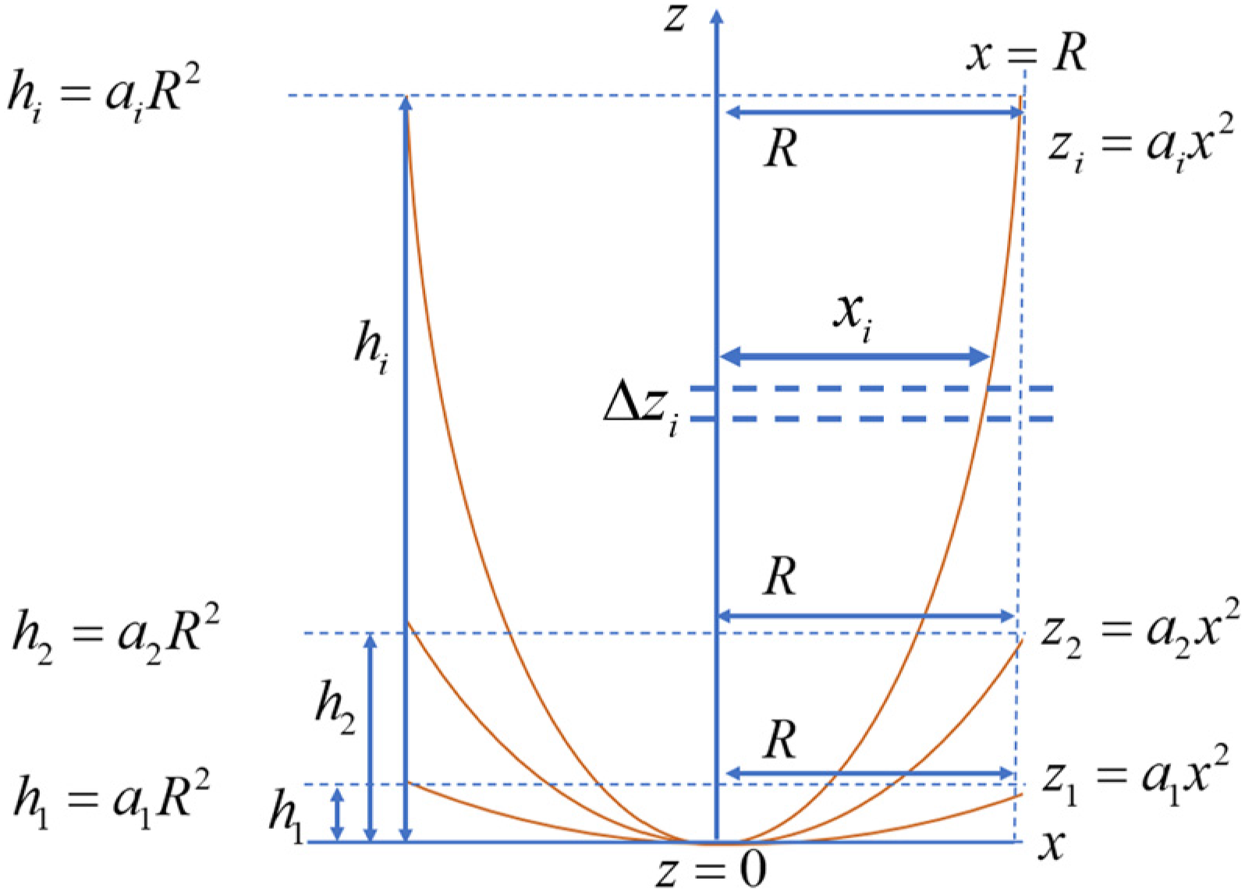
Parabolas in terms of its height (thickness) h, shape factor a, and growth-base radii R.
Rotating the parabola with respect to z as its axis for half of a revolution will result in a three-dimensional parabola. We may derive the equation of the parabola volume V by letting 
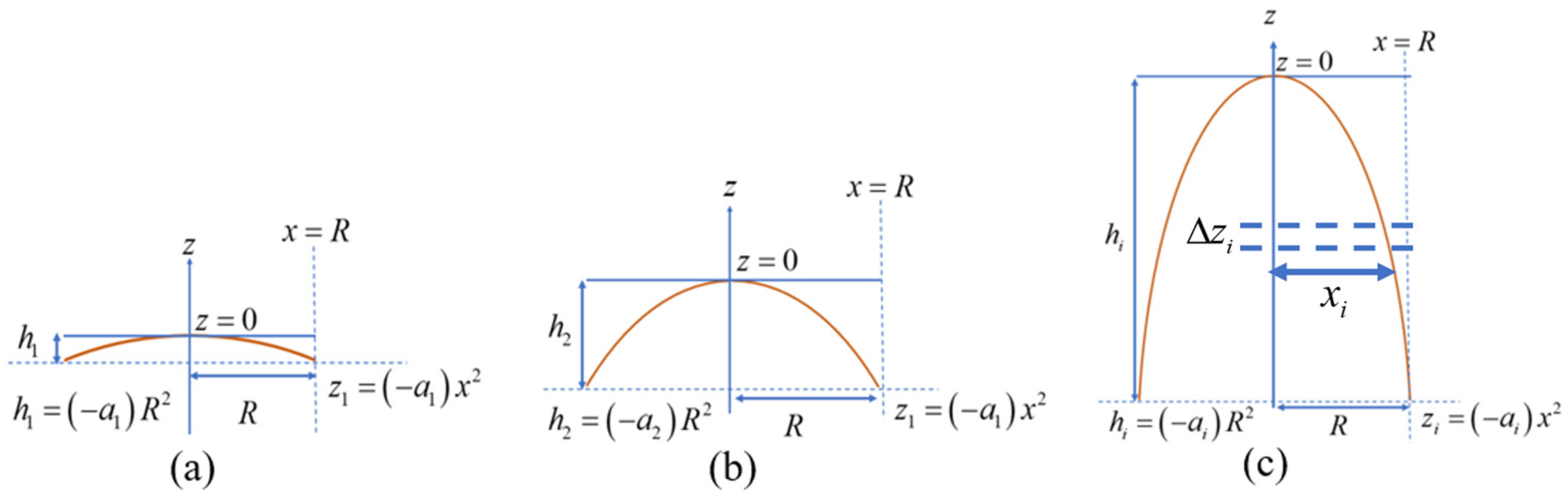
The evolution of growth from height or growth thickness of: (a)
Mathematically the negative parabola reorientation does not affect calculation for the parabolic volume. The volume calculated using the method for Figure 3 for equations (11) and (12) is equal to the volume calculated for Figure 4. Thus, the expression for the volume of the negative parabola is the same as equation (12). Since from the parabolic equation x can be rewritten in terms of z and the parabolic shape factor a as 

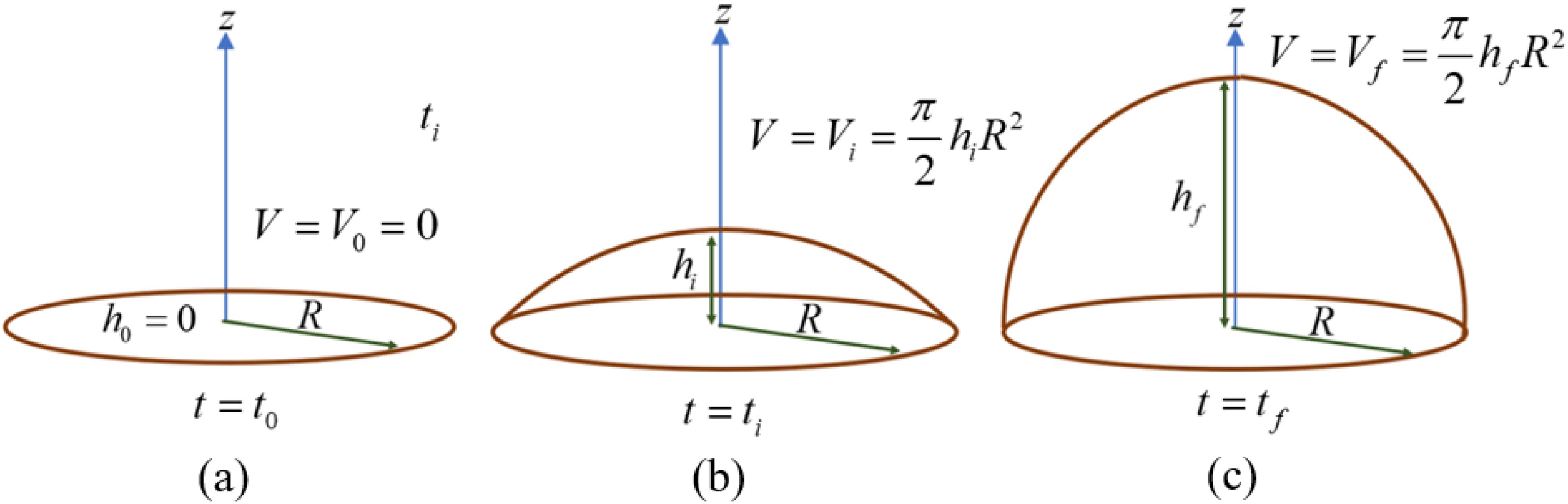
The growth evolution governed by the rate of growth expression within the time of: (a)
Figure 5(a)–(c) shows three stages of the growth evolution governed by the rate of growth expression within the time of
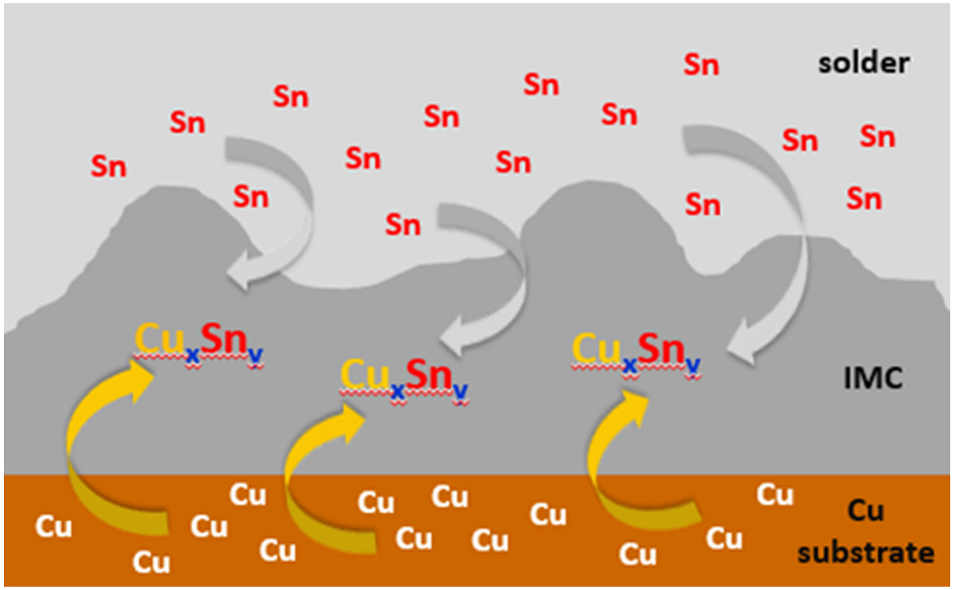
Schematic showing IMC layer growth due to diffusion elements of Cu and Sn.
Deduction of the grain growth kinetics by the Burke and Turnbull analysis was based on the assumption where the driving pressure P on the boundary arises from the curvature of the boundary. It has stated that the driving pressure is a summation of two different pressures correspond to the boundary of energy 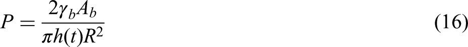

To further analyse the growth behaviour of IMC layer, the source of IMC layer formation is illustrated in Figure 6. The formation of the IMC layer depends on the source of Sn and Cu. Cu mainly comes from the Cu substrate, whereas Sn comes from the solder. 47 Obviously, this formation and growth of the IMC layer differ from the normal grain growth as analysed by Burke and Turnbull. This is because the IMC layer is a phase formed from different elements, in this case, Cu and Sn, and the IMC phase layer then continues to grow owing to the continuous reaction assisted by thermally activated process. Another interesting feature is that in normal grain growth, the growth process occurs along three directions (3D growth) as contrast to the IMC layer growth, the growth occurs along one direction towards the solder matrix (one-directional growth). Thus, this directional or one-directional growth should be considered in assessing IMC layer metallurgical electronic interconnection.
Detailed analysis on directional growth has been simplified using the schematic in Figure 7, to show a comparison between normal grain growth occurring in three dimensions (3D: x, y, and z-directions) and IMC layer growth only occurring in the z-direction (one-directional, 1D). The IMC layer grows only along the z-direction, that is, towards the solder matrix area. For normal grain growth process, surface tension is considered to minimise the area/energy to accommodate thermodynamic stability of grain. However, for IMC layer growth, surface tension is playing less important role because of the nature IMC layer shapes, which result from the reactions between different elements.
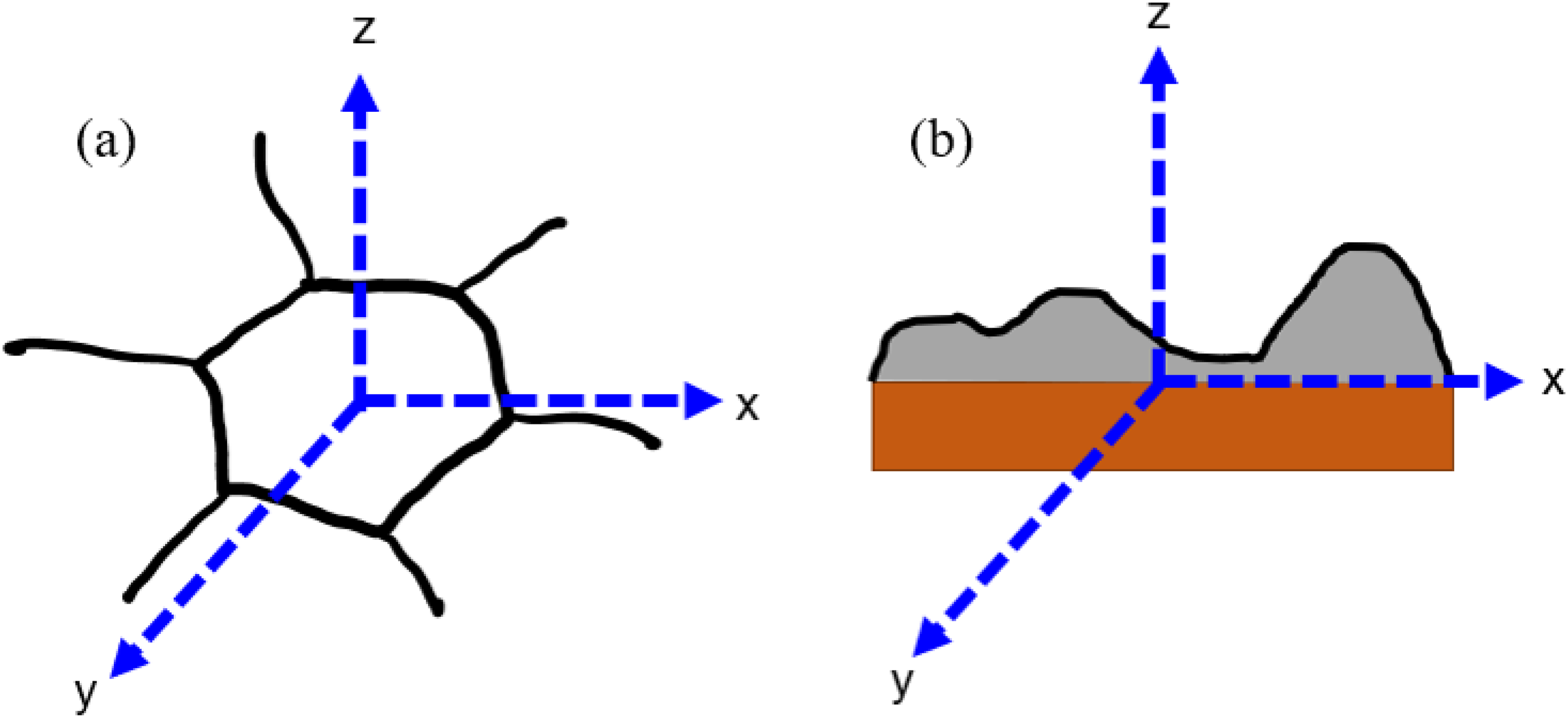
Schematic of comparison between: (a) normal grain growth in three-dimension (3D) versus IMC layer growth in one-directional (1D) towards the z (+ve) direction only.
From this analysis, it is clear that the growth behaviour does not reflect the parabolic shape of the IMC layer as shown in the mathematical expression modeling but grows consistently perpendicular to the substrate, that is, towards the solder matrix area. The origin of the growth model, especially for grain growth, typically follows the “shape” factor, such as topological approach and space-filling, and grows in x, y, and z (3D) directions. Therefore, the growth behaviour deviates from the normal grain growth theory, and this finding suggests that the parabolic growth model is inadequate to explain the growth of the IMC layer subjected to isothermal aging. This linear behaviour of IMC layer growth subjected to isothermal aging provides valuable insight in terms of stability and prediction of solder joint reliability. On the other hand, for example, in transient liquid phase (TLP) bonding, the linear growth behaviour of the IMC layer is preferable because the IMC formation is tailored to be homogenous in between metallic sandwich structures. 48 This will have a significant effect on the mechanical, i.e., robust joining, thermal, and electrical properties of the solder joint. The understanding of the IMC layer growth behaviour can contribute knowledge-specific applications and thus be useful for better reliability and lifespan of the electronic components.
Conclusion
In summary, the growth of the IMC layer of SAC 0307 on a Cu substrate has been investigated through a HTS test at 150°C up to 2000 h. A linear relationship is observed between the IMC layer thickness and HTS time, beyond the typical reliability testing time. This finding shows that the IMC layer follows the linear growth behaviour which has deviated from the typical claim of the parabolic growth law. This finding suggests that the parabolic growth law is inadequate to thoroughly explain the IMC layer growth in electronic metallurgical interconnections. The IMC layer growth involved growth in one direction, thus deviating from the typical parabolic growth law which is based on the normal grain growth theory, proposed by Burke and Turnbull.
Footnotes
Declaration of conflicting interests
The authors declared no potential conflicts of interest with respect to the research, authorship, and/or publication of this article.
Funding
The authors disclosed receipt of the following financial support for the research, authorship, and/or publication of this article: The authors would like to acknowledge the financial support provided by the Ministry of Higher Education, Malaysia (grant number FRGS/1/2019/STG07/UKM/03/1) and Universiti Kebangsaan Malaysia for research facilities.