
Abstract
Fluorinated polyimide materials were selected for their exceptional flexibility, high thermal stability, and minimal absorption loss. These materials were subsequently employed in the production of single-mode polymer optical waveguide devices using photolithography. In this study, a fluorinated polyimide material doped with NaYF4 nanocrystals was prepared and confirmed to exhibit low absorption loss near 1550 nm, which is within the common communication window. The refractive index of the fluorinated polyimide films was precisely adjusted by the NaYF4 doping, the adjustable ranges for the refractive index were 1.95% and 1.72% for doped and undoped, respectively. Secondly, utilizing the NaYF4 nanocrystals doped-fluorinated polyimide materials, a three-layer single-mode polymer optical waveguide device for C-band (near 1550 nm) optical interconnection was fabricated by etching the underlying cladding and employing silicon nitride as a mask. The transmission performance of the device was excellent, with a total waveguide coupling and transmission loss of 1.502 dBm.
Introduction
With the rapid development of electronic information technology, internet technology is becoming increasingly integrated into our daily lives, and people have higher demands for information processing speed, transmission capacity, and information security. Optical fiber communication technology is widely used for long-distance information transmission. In recent years, there have been steady improvements in information transmission capacity and speed with the gradual upgrade of wavelength division multiplexing systems (WDMS) and advancements in microelectronics semiconductor technology, leading to significant improvements in board size and integrated circuit density. However, traditional electrical interconnection technology, due to physical limitations, produces parasitic effects, signal delays, crosstalk, and high power consumption. Consequently, this limits the further enhancement of information transmission capacity and speed. As a result, optical interconnection is garnering increasing attention as an alternative to electrical interconnection, utilizing light beams instead of traditional metal wires for information transmission.1,2
Currently, optical interconnection technology can be classified into three types: fiber-based, free space, and optical waveguide-based. (1) Fiber-based optical interconnection technology relies on the connection between optical fibers and photoelectric devices. It offers advantages such as low cost, simple structure, and mature technology, making it widely used in cabinet-level optical interconnection. However, there are compatibility issues between fiber embedding and the traditional Printed Circuit Board (PCB) fabrication process. The traditional PCB fabrication process requires high temperature (170 °C–180 °C) and high pressure (15 kPa/cm2), which can cause stress deformation and oxidation degradation in the fiber. (2) Free-space optical interconnect technology allows for optical path conversion and reconstruction, offering great flexibility. However, it is only suitable for very short-distance or unimpeded transmission lines, such as between chips, as large transmission losses may occur otherwise. In board-level optical interconnection systems, free-space optical interconnection requires high environmental conditions and assembly accuracy, making it unsuitable for practical use. (3) Optical waveguide-based interconnection technology enables complex functions like beam splitting, routing, and filtering without considering fiber routing and embedding. The preparation of waveguide devices with silica material is relatively mature, with many preparation methods and low transmission loss. However, for plate-level optical interconnection, it needs to be prepared in a large area, which increases cost, and the refractive index of the material has a limited adjustable range, it is most appropriate to control the refractive index difference between the core and the cladding between 0.01 and 0.05. Other materials, such as InP, Ge, and AsGa, have advantages in the fabrication of active devices, but the cost of large area fabrication is also extremely high. Overall, optical waveguide-based interconnection technology possesses the advantages of high process compatibility and no transmission line limitation, making it the most suitable method for realizing optical signal transmission in the current board-level optical interconnection system. Polymer materials show promise for optical interconnection technology based on optical waveguides due to their versatility, low cost, and suitability for large-area fabrication.3,4
The application of polymer materials in optical waveguide optical interconnection requires high thermal stability, stable and controllable refractive index, low surface roughness, and minimal absorption loss in the near-infrared communication window. These properties ensure better integration of subsequent waveguide device preparation onto the plate, precise design of device structure, and minimal optical transmission loss. Traditional optical polymer materials include polymethyl methacrylate,5–8 polystyrene,9,10 polycarbonate,11,12 polyurethane,13,14 and epoxy resin,15–17 which are easy to prepare, obtain raw materials, and are cost-effective. However, most of these are thermoplastic materials with poor heat resistance. Moreover, they exhibit significant optical absorption loss in the infrared communication window, limiting their application as optical waveguide materials.
Polyimide (PI) is one of the most thermally stable polymers available. Its major advantage lies in its high photothermal stability and chemical stability.18,19 However, it suffers from inadequate light transmittance.20,21 Traditional PI is brown or dark yellow and unsuitable for use in optical waveguides at 1550 nm wavelength. The color is derived from the charge transfer effect between the electron donor (diphenyl ether unit) and electron acceptor (dianhydride unit) in the backbone of PI. This effect causes tightly packed molecular chains, resulting in strong absorption in the visible light and near-infrared range and making dissolution and subsequent molding operations difficult. Therefore, preliminary preparation and property exploration of selected fluorinated polyimide materials are necessary in this work.22,23 In this paper, we utilize the properties of NaYF4 nanoparticles on PI through modified doping, not only to ensuring PI film good photothermal stability, but also its light transmittance and this refractive index have also been adjusted. NaYF4 is often used as the host crystal because it is known as one of the best host materials for lanthanide ions (guest). The guest materials, especially lanthanide (III) ions, are known to play an important role in the up- or downconversion of luminescence. Therefore, it can play the role of adjusting the refractive index of PI material.
In this paper, based on polymer PI, we prepared fluorinated polyimide materials doped with NaYF4 nanocrystals, the optimal doping concentration is 20%, exhibiting good high-temperature resistance and adjustable refractive index. Using the fluorinated polyimide doped with NaYF4 nanocrystals materials, we fabricated a three-layer single-mode polymer optical waveguide device for the C-band (near 1550 nm) optical interconnection by etching the underlying cladding and using silicon nitride as a mask. This device demonstrates excellent transmission performance, with a total waveguide coupling and transmission loss of 1.502 dBm.
Experimental
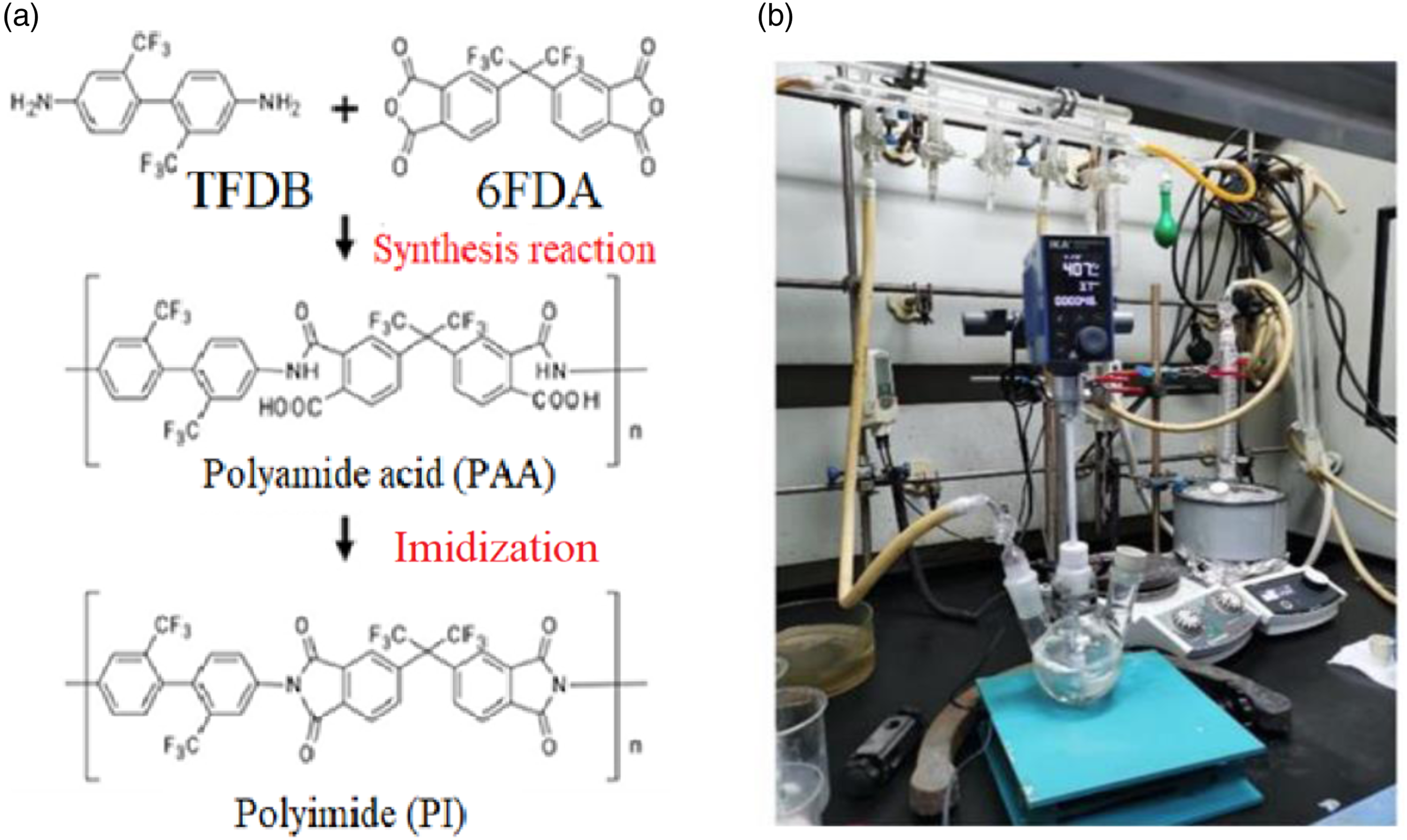
Synthesis of polyamide acid
4,4'-(Hexafluoroisopropylidene)bis (phthalic anhydride) (6FDA) is a typical monomer used in the synthesis of fluorinated polyimides. It is an acid dianhydride with a curved structure, which imparts high transparency and reduces the birefringence effect in the synthesized fluorinated polyimides. On the other hand, 2,2'-bis(trifluoromethyl)benzidine (TFDB) contains a rigid biphenyl skeleton, contributing to a high glass transition temperature (Tg) in the resulting fluorinated polyimide. Therefore, these two monomers were chosen as preliminary research materials for the application of polymer optical waveguides. The synthesis steps for polyamide acid are described below, and the reaction formula and device setup are illustrated in Figure 1(a) and (b). (1) In a three-necked flask, 50 mL of anhydrous dimethylacetamide (DMAC) solvent was added, followed by the addition of 5g of TFDB (156.14 mmol) into the solvent. The solution was stirred at 100 rpm under nitrogen protection until the TFDB completely dissolved, resulting in a colorless and transparent solution. (2) 6.93g of 6FDA were added into the above transparent solution, divided into 5 times, each time adding 1.386g of 6FDA; Then, under the protection of nitrogen, it was mechanically stirred at 100 r/min until the 6FDA powder was completely dissolved;Repeat the operation, and wait until the last 6FDA powder was completely dissolved before adding the next time until the final dissolution was complete. (3) Once the solution clarified from step (2), the stirring speed was increased to 400 rpm, and the reaction was carried out at 25°C for 22 h, and got this Polyamide acid(PAA) solution. (4) The PAA was transferred into a clean glass bottle and stored in the refrigerator at 0 °C–10 °C until further use. (a) Reaction formula and (b) device for polyimide synthesis.
Synthesis of NaYF4 nanocrystals doped with rare-earth elements
Nanocrystals (NCs) were prepared using a procedure described in previous studies, with some modifications.24–29 All experiments were conducted under an argon atmosphere using standard Schlenk techniques. In a typical synthesis, fixed amounts of Er3O3 (14.34 mg, 0.0375 mmol) or Yb2O3 (147.78 mg, 0.375 mmol) and Y2O3 (330.25 mg, 1.4625 mmol) were mixed with 50% aqueous trifluoroacetic acid (15 mL) and heated to 80°C to obtain the lanthanide trifluoroacetate precursors. The residual solvents were evaporated under vacuum at 70°C. The molar composition of the feed external solution was [Er/(Er + Yb + Y)] = 2 mol%. Subsequently, the lanthanide trifluoroacetate precursors were added to a three-necked flask containing octadecane (30 mL), oleic acid (30 mL), and sodium trifluoroacetate (0.51g, 3.75 mmol). The solution was heated to 110°C under vacuum with stirring for 30 min, and the flask was purged with argon at 10-min intervals to remove water and oxygen. The resulting yellow solution was then heated to 300°C under argon with vigorous stirring for 30 min. After cooling to room temperature, the mixture was precipitated using acetone in an ultrasonic bath and collected by centrifugation at 11,000 r/min for 30 minutes. The precipitate was washed with ethanol, and the nanocrystals were finally dispersed in 5 mL of chloroform. The resulting NCs exhibited colloidal stability in organic solvent for weeks without visible aggregation or settling.25,27–29
The morphology and the particle size distribution of the nanoparticles have been examined by transmission electron microscopy. Figure 2(a) and (b) displays the TEM image of the dispersion of synthesized NaYF4 nanoparticles in DMAC and PPA solvent. Figure 2(c) shown the X-ray diffraction (XRD) patterns of the NaYF4: Yb3+, Er3+, material with different calcination time. From the XRD pattern, diffraction peaks at 2θ = 17.26, 30.02, 30.8, 43.5, 53.22, 53.68 of all four samples are matched well with the (100), (110), (101), (201), (300), (211) peaks of β-NaYF4 phase structure. The diffraction peaks at 2θ = 28.78, 47.8, 56.66 for the samples calcined for 2 h and 4 h are in good agreement with the (111), (220), (311) peaks of the α-NaYF4 phase structure.
30
This result shown coexistence of β-NaYF4 and α-NaYF4 phase structure of synthesized NaYF4: Yb3+, Er3+, material calcined for 2 h and 4 h. The NaYF4: Yb3+, Er3+, materials calcined for 6 h and 8 h have only β-NaYF4 phase structure. All the XRD plots have shifting of characteristic peaks indicating the doping, and their full width at half maximum can also be seen for the interstitial voids positions and doped Yb3+ and Er3+ ions at different calcination temperatures. This can also be confirmed by the fourier infrared spectroscopy of Supplementary Figure S1 in the supporting information. At 10 K, the measured Yb3+ absorption spectra have sharp peaks at 10236 cm−1 (977 nm) for β− NaYF4:Yb/Er. The shift in the absorption peaks is due to the different crystal structures of the host materials, which provide different crystal field potentials to the lanthanide ions. At 297 K, the absorption spectra are similar, albeit having broader spectral linewidths because of phonon-induced dephasing and multiphonon relaxation at higher temperatures. In this study, we focused only on the doping and dispersion of NaYF4 nanoparticles in PI, the nanoparticle sizes were measured (from Figure 2(d) for over 100 nanoparticles), and the size distributions were fitted to a log-normal distribution (Figure 2(d)), which resulted in an average diameter value of 24 ± 4 nm. Different volumes of the mother liquor of rare-earth nanoparticles were withdrawn and added to a small bottle containing a PAA solution, followed by the addition of a magnetic stirrers. The bottle was then sealed with sealant. By stirring the mixture on a magnetic stirring table for 12 h, a PAA solution with evenly dispersed nanoparticles was obtained. Figure 2(b) shows the TEM image of the dispersion of. (a) TEM image of NaYF4 nanoparticles in DMAC solvent dispersion, (b) TEM image of NaYF4 nanoparticles in PAA solvent dispersion, (c) XRD Characterization results of α- and β-phase and NaYF4: Yb3+, Er3+ (d) the corresponding size distribution histograms of the nanoparticles.
NaYF4 nanoparticles in the PAA solution. It is evident that the nanoparticles are uniformly dispersed without any agglomeration. Other optical characteristic of 20% doping concentration of NaYF4: Yb3+, Er3+-doped PI films shown in the supporting information of Supplementary Figure S2 and S3.
Preparation of NaYF4 nanocrystals doped polyimide films
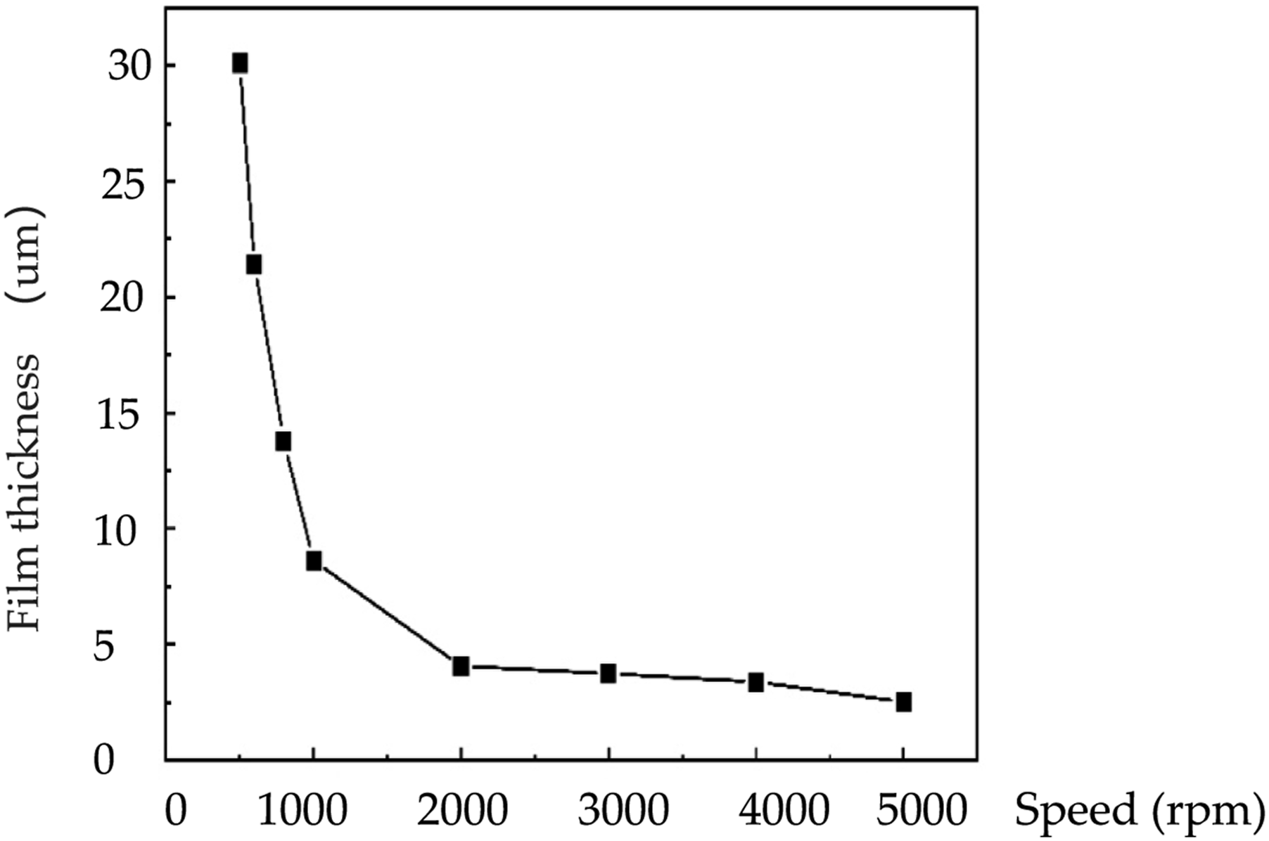
The materials used for fabricating polymer optical waveguide devices need to exhibit good film formation and smooth film surfaces to avoid introducing high optical losses. Therefore, we adopted a spinning method to prepare the polyimide films doped with the NaYF4 nanocrystals by spinning a -polyamide acid (PAA) solution on a glass substrate, followed by drying and heating it up to 300°C with a gradient. The Schematic diagram of NaYF4 doped polymer PI see the supportinsg information of Supplementary Figure S3, the specific steps are as follows: (1) To ensure the flatness of the film, the substrate was thoroughly cleaned. In this experiment, the glass substrates were sequentially soaked in acetone, isopropanol, deionized water, and ethanol (in the specified order), and subjected to ultrasonic treatment for 15-20 min. Finally, the substrates were dried using a nitrogen gun to achieve a clean and dry surface. (2) Take 350 mL PAA solution containing NaYF4 nanocrystals, subsequently, a significant amount of PAA solution was deposited onto the glass substrate using a pipetting gun. By selecting appropriate rotation speed and time, films of different thicknesses were prepared. Figure 3 illustrates the relationship between the thickness of the self-synthesized PAA solution-based polyimide film and the spin coating speed. When the spin speed exceeded 2000 rpm, an initial step was added, typically involving a spin coating at 600 rpm for 5-10 s to ensure even distribution of the solution on the substrate. (3) The NaYF4 nanocrystals-doped PAA (PAANc) coated substrates were then placed in a programmable oven with temperature control. After surface drying at 80°C for 30 min, the temperature was gradually increased in steps of 50°C, with each step lasting 30 min. This thermal curing and imidization process resulted in the formation fluorinated polyimide doped with the NaYF4 nanocrystals (PINc) thin films. Relationship between polyimide film thickness and rotational speed.
Results and discussion
Characterization of properties of NaYF4 nanocrystals doped-fluorinated polyimides
Molecular weight test
To ensure the thermal stability and mechanical properties of polyimide films, it is important to obtain polymers with the largest possible molecular weight. 31 The relationship between viscosity (η) and polymer molecular weight (M) can be expressed by the formula [η] = 1.85 × 10⁻⁴ M0.80. 32 The molecular weight of the polymer also affects the viscosity of the solution. Higher molecular weight leads to increased viscosity of the solution.
Test results of thin film molecular weight at different degrees of imidization.

The molecular weight of a polymer can be determined using various statistical measures such as number-average molecular weight (Mn), weight-average molecular weight (Mw), and Z-mean relative molecular weight (Z). Mn is the sum of individual molecular weights of each polymer chain divided by the total number of polymer chains in the sample and provides information about the molecular weight distribution of the polymer. On the other hand, Mw is the sum of individual molecular weights of each polymer chain multiplied by the weight fraction of that chain, divided by the total weight of the sample. It also gives insights into the molecular weight distribution. Mn is particularly useful for polymers with a narrow molecular weight distribution, whereas Mw is more suitable for polymers with a wide molecular weight distribution. The polydispersity index (PDI), calculated by dividing Mw by Mn, indicates the broadness of the molecular weight distribution.
To compare the degree of polymerization under different conditions, the results of the numerous-mean relative molecular mass test were used as a basis for comparison. As the imidization temperature increased, the degree of polyimide film completion and the number-average molecular weight gradually increased, indicating an increase in the degree of polymerization. This can be attributed to the formation of charge migration complexes between polyimide molecular chains, Preferred Layer Packing (PLP), and other inter-chain interactions during the imidination process, which result in closer inter-chain binding and polymers with a higher degree of polymerization. Additionally, the gel permeation chromatography (GPC) analysis of NaYF4 nanocrystals doped-PAA determined a molecular weight of 7.90×10⁴ for the completely imidized polyimide film. This high degree of polymerization meets the basic requirements of optical waveguide devices.
Thermal performance analysis of NaYF4 nanocrystals doped PAA
To assess whether the thermal properties of the synthesized PI/PAA meet the requirements for preparing polymer optical waveguide devices in this project, we conducted Thermo Gravimetric (TG) and Differential Thermal Analysis (DTA) using the Diamond TGA/DTA instrument from Platinum Elmer Instruments (Shanghai) Co., Ltd. The analysis involved testing the synthetic PAA solution under different atmospheric conditions including air, argon, and nitrogen. Figure 4 present the combined TG/DTA profiles that illustrate the thermal degradation characteristics of NaYF4 nanocrystals doped-PAA solution at a heating rate of 10°C/min for each atmosphere. For the analysis, a sample weighing 200 mg was measured in dry air, argon gas, and nitrogen, respectively. The sample underwent a heating process from room temperature to 800°C at a rate of 10°C/min after an initial heating to 150°C to remove adsorbed water. (a) TGA and DTA curves of NaYF4 nanocrystals doped-PAA solution in air; (b) TGA and DTA curves of NaYF4 nanocrystals doped-PAA solution in argon; (c) TGA and DTA curves of NaYF4 nanocrystals doped-PAA solution in nitrogen.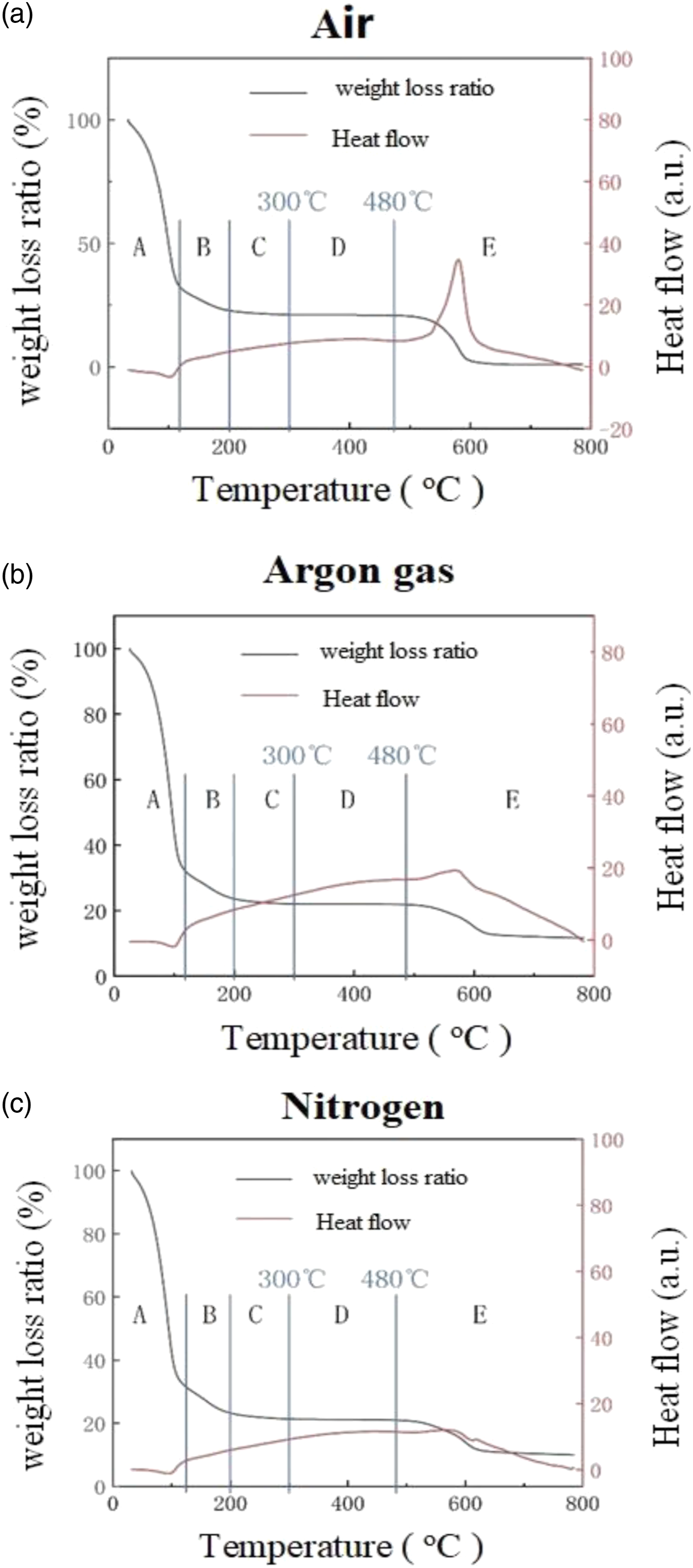
Figure 4 demonstrates that the atmosphere during solvent evaporation and amination does not significantly affect the decomposition process. The TGA and corresponding derivative thermogravimetric (DTG) curves of NaYF4 nanocrystals doped-PAA are depicted. The curves reveal three weight loss stages in the doped PAA. The first stage, occurring below 150°C, can be attributed to moisture evaporation. 35 The second stage, spanning 150-480°C, corresponds to the decomposition of carboxylic acid groups in PAA. 36 The final stage, occurring between 480 and 800°C, represents the formation of the imide cycle, accompanied by the elimination of water, which aligns.
With the five stages of PI states: solvent volatilization (A), rapid imidization (B), slow imidization (C), imidization finish (D), and polyimide decomposition (E). The end point of the slow imidization stage, around 300°C, indicates that the set imidization temperature of 300°C achieves complete imidization during the PAA synthesis. Moreover, the PI decomposition temperature reaches 480°C, confirming the excellent heat resistance of the synthesized PI/PAA. Notably, the heat flow curve exhibits a prominent heat absorption peak near 580°C, which corresponds to the relatively complete decomposition temperature of polyimide in the TG ratio curve.
Film flatness testing
Special attention should be given to the flatness and uniformity of the polymer spin-coated film during the preparation of the polymer optical waveguide, as it directly impacts the transmission loss of the subsequent fabricated devices. Atomic Force Microscopy (AFM) can be used to examine polymer films prepared by spin coating.
In this study, AFM analysis was conducted on completely imidized fluorinated polyimide films at 300°C. The results are presented in Figure 5. Within the size range of 10 μm × 10 μm, the root mean square roughness (Rrms) of the films was measured to be only 1.689 nm, and the maximum fluctuation height (Rz) was determined to be 59.136 nm. In a smaller range of 2 μm × 2 μm, the Rrms value of the RMS roughness was found to be 0.844 nm, with a maximum fluctuation height of 20.870 nm. Based on the aforementioned measurements, it can be con-cluded that the roughness level is significantly below λ/10 (λ = 1550 nm), which ensures minimal Rayleigh scattering loss and satisfies the requirements for fabricating optical waveguide devices. (a) Three-dimensional picture of AFM results of films in the range of 10 μm × 10 μm; (b) Three-dimensional AFM results of films in the range of 2 μm × 2 μm.
Infrared characterization test of materials
In this study, the infrared absorption characteristics of two types of fluorinated polyimide films were examined: NaYF4 nanocrystals-doped fluorinated polyimide film (referred to as FPI-1) prepared using self-synthesized PAA solution, and fluorinated polyimide film (referred to as FPI-370) prepared using Hylimide®STPI370 transparent polyamide acid liquid material. The latter was obtained from Wuhan Emide New Material Technology Co., LTD for the purpose of material comparison. Both films were prepared using the same thermal imidization procedure, and their refractive indices were measured at Wuhan Yiguang Technology Co., LTD. To assess the prepared fluorinated polyimide films (FPI-1 and FPI-370), it was necessary to investigate their absorption in the near infrared range and determine the success of the preparation process, particularly in terms of absorption within the required near infrared communication window. For this purpose, the Nicolet iS50R Fourier transform infrared spectrometer FT-IR from Thermo Scientific Company in the United States was used to conduct infrared absorption testing using the attenuated total reflection (ATR) method.
Figure 6 displays the infrared absorption spectra of both film samples. Both samples exhibit a prominent absorption peak at 750 cm−1, which corresponds to the deformation and bending vibration of the imide ring. The clear absorption peaks at 1248 cm−1, 1373 cm−1, and 1781 cm−1 are attributed to the C-O stretching vibration of the imide ring, the symmetric stretching vibration of imide C-N, and the asymmetric stretching vibration of imide C=O, respectively. Notably, the peak at 1170 cm−1 represents C-F absorption. These findings align with results reported in other literature,
37
confirming significant imidization during the gradient heating preparation process of the thin films. However, Figure 6 does not exhibit absorption characteristic peaks of PAA, such as the amide N-H bending vibration absorption peak at 1543 cm−1, the C-N/N-H coupling deformation vibration absorption peak at 1500 nm, and the anhydride C=O stretching vibration absorption peak at 1700 cm−1. This suggests that complete imidization has occurred, with no residual PAA present in the final film. Additionally, there is no observable solvent absorption peak over 1800 cm−1, indicating complete solvent volatilization. Fourier infrared absorption spectra of FPI-1 and FPI-370 films.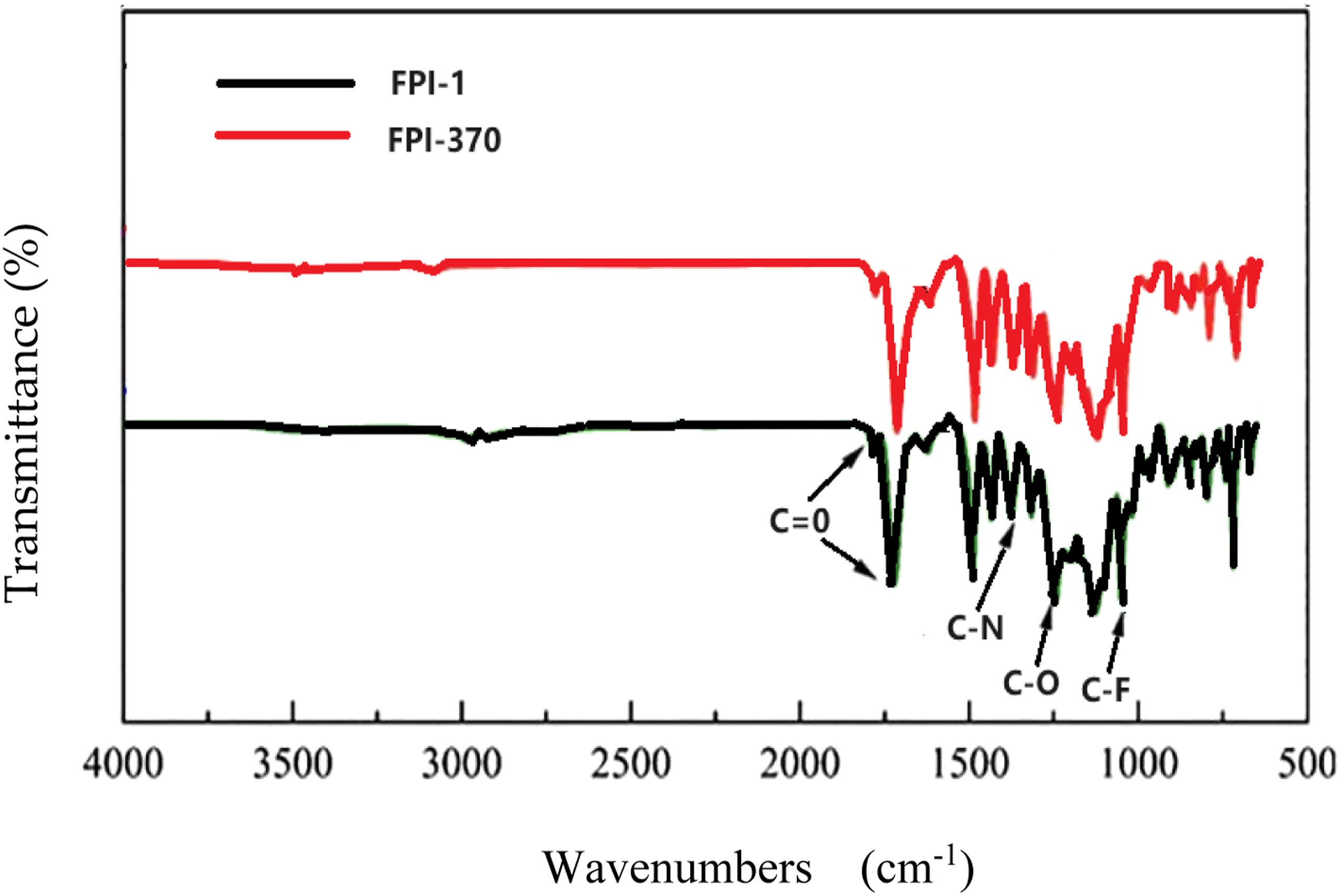
Furthermore, Figure 6 reveals that there is no obvious absorption peak near the low loss window of 1550 nm communication. The high transmittance in these regions indicates minimal absorption loss in the fluorinated polyimide materials FPI-1 and FPI-370 within the two communication windows. This establishes them as suitable materials for fabricating optical waveguide devices used in plate-level optical interconnection.
Fine adjustment scheme for refractive index
To meet the requirements of designing and fabricating single-mode optical waveguide devices with different sizes, it is crucial to accurately adjust the refractive index difference between the core and cladding materials within a specific range. By replacing hydrogen atoms with fluorine atoms in the molecular chain structure of polyimide, not only can the absorption loss of the material in the communication window be reduced, but the refractive index can also be precisely adjusted based on the fluorine content. This adjustment is possible because the volume of a fluorine atom is larger than that of a hydrogen atom, and its introduction increases the free volume of the molecule, thereby reducing the refractive index of the polymer.
38
Furthermore, the polarizability of C-F is lower than that of C-H, and the refractive index can be further reduced by decreasing the polymer's polarizability.
39
To accurately adjust the refractive index of the self-synthesized solution (fluorinated polyamide acid without NaYF4 nanocrystal doping) for film preparation, a diamine monomer with a similar structure to TFDB but slightly lower fluorine content was selected. This monomer was then polymerized with 6FDA to form FPI/PPAA-2 in various mass ratios, and the resulting polyimide films were prepared for refractive index testing. The results are depicted in Figure 7(a) and (b). (a) Refractive index test results of films with different fluoride content (FPI/PAA-2 mass fraction), (b) Refractive index of the film at 1550 nm varies with fluorine content (FPI/PAA-2 mass fraction).
The film's refractive index increases with the increase in the mass fraction of FPI/PAA-2, corresponding to a decrease in fluorine content. These findings are consistent with the literature, and the range of refractive index adjustment reaches 1.95%, indicating the feasibility of this refractive index adjustment method.
In this study, a novel approach to refractive index adjustment was discovered, which involves the uniform doping of rare earth nanoparticles to enhance the refractive index of thin films. PAA solutions with varying doping concentrations were spin-coated onto glass substrates, and through gradient heating and iminization, fluorinated polyimide films with different concentrations of rare earth nanoparticles were prepared. The results of refractive index testing are illustrated in Figure 8(a) and (b). (a) Refractive index test results of thin films with different nanoparticle doping concentrations, (b)The refractive index of the film at 1550 nm changes with the doping concentration of nanoparticles.
The test results demonstrate that the refractive index curves of the doped films with different concentrations smoothly decrease as the wavelength increases, indicating even dispersion of the nanoparticles within the films and uniform refractive properties. At 1550 nm, the refractive index of the nanoparticle-doped films significantly increases compared to that of the undoped FPI/PAA-2 films. However, as the doping concentration reaches a certain level, this increasing trend gradually levels off, and with further increases in doping concentration, the refractive index of the film begins to decline.
Measurement of optical waveguide performance
For details about how to prepare optical waveguides, see the supporting information of Supplementary Figures S4–S7. In this study, the end-face coupling method was employed to perform a near-field spot test on the prepared single-mode optical waveguide device, aiming to gain preliminary insights into its light collection and propagation capabilities. The system diagram of the test setup is presented in Figure 9. The test system consists of an infrared light source, a fiber tuning system, a visible light observation system, and an infrared CCD observation system. The infrared light source used was the Santec TSL-710 high-performance tunable laser, which offers an ultra-wide tuning range of 1480 to 1640 nm, an output line width of less than 100 kHz, and a maximum output power of +13 dBm. The XYZ 3D precision microactuator was utilized to precisely adjust the alignment displacement between the single-mode fiber and the waveguide device. The infrared CCD viewing system included a 4F system focusing objective and a Goldeye SWIR model P008 camera equipped with a high-performance InGaAs sensor, highly responsive in the near-infrared and shortwave infrared spectra ranging from 900 nm to 1700 nm.
40
Schematic diagram of waveguide near field spot test system.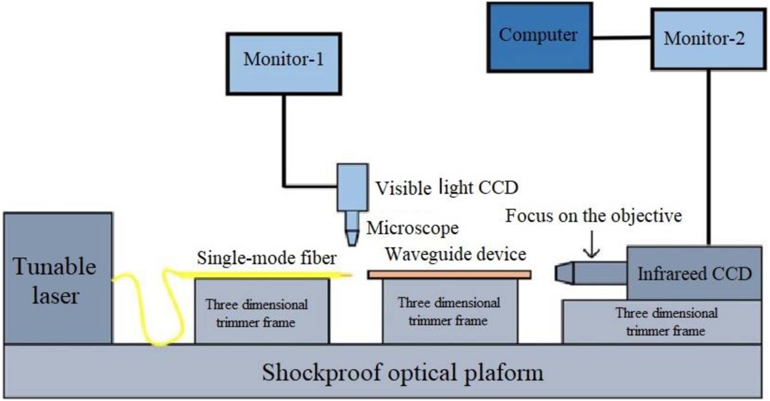
Figure 10(a) and (b) illustrate the results of the near-field spot test conducted on two different waveguides on sample A1, while Figure 10(c) depicts the near-field spot test results of the waveguides on sample A2. The output optical power of the laser was fixed at 0 dBm, and the length of the test waveguide was set to 1.5 cm. It can be observed that both test waveguides on sample A1 exhibited a certain ability to concentrate light through the waveguide, with the waveguide beam ability on sample A1 being noticeably superior to that on sample A2. As shown in Figure 10(a)–(c), the optical fiber fixed in the V-groove was coupled into the waveguide of the sample, secured in the carrier stage through vacuum adsorption. After propagating through the waveguide, the light was coupled out by another optical fiber. The loss incurred during this process was determined by the power meter reading. Accurate alignment of these two couplings was crucial as misalignment could result in significant coupling losses, thereby affecting the test results. Therefore, prior to the formal test, a red laser pointer was commonly employed as the light source to connect the incident fiber, and the 3D trimmer on both sides was adjusted accordingly. In the visible light observation system, light could be coupled into the waveguide, revealing a red propagation track on the waveguide's surface, as depicted in Figure 10(d). (a)–(c) Results of near - field spot test of waveguide device, (d) Waveguide coupling and transmission loss test system and red light alignment.
Once the laser was replaced to connect the incident fiber, and the output optical power was fixed at 0 dBm, the two trimmers were fine-tuned further until the connected outgoing fiber yielded the highest optical power reading on the power meter. Based on the test results obtained from sample A1, the optical power of the laser output signal light after connecting the fiber and the attenuator was -8.698 dBm. The optical power after coupling and waveguide transmission was -10.20 dBm, indicating a total waveguide coupling and transmission loss of 1.502 dBm.
Analysis of waveguide coupling loss
The optimal coupling between a waveguide and a fiber aims to achieve the highest coupling efficiency and maximize the output optical power. This helps increase the transmission distance and improve the signal-to-noise ratio in optical interconnection. Currently, the losses measured using the end-face coupling method include coupling losses and transmission losses, with a focus on the reasons for coupling losses in this discussion.19,41,42 (1) Mismatch Loss: The mode field distribution plays a significant role in generating cou pling losses. The energy from the fiber is coupled into the waveguide through the matching of the optical fiber mode field and the waveguide mode field. However, due to differences in the preparation, materials, and sizes of the waveguide and fiber, their mode field distributions are different. As a result, losses occur due to mode field mismatch, which are challenging to avoid. (2) Figure 11(a) illustrates that when the waveguide end face is perpendicular to the fiber, the lateral tilt of the waveguide section during manual cutting prevents full coupling of light from the fiber into the waveguide. Instead, it remains at a certain angle with the on-chip strip waveguide. Similarly, Figure 11(b) demonstrates that the longitudinal tilt of the waveguide section during manual cutting results in incomplete alignment of the fiber with the on-chip waveguide end face during coupling. Consequently, the misalignment loss caused by manual cutting deviations is the primary reason for the large and inconsistent coupling loss observed in the waveguide prepared for testing in this study. This misalignment significantly affects the subsequent loss test results. Therefore, there is a need for improvement in the current end-surface treatment method. (a) Schematic diagram of lateral tilt caused by manual cutting and visible CCD, (b) Schematic diagram of longitudinal tilt caused by manual cutting and visible CCD.

Conclusions
This article focused on the practical application requirements of polymer optical waveguide devices in plate optical interconnection and conducted a preliminary exploration of NaYF4 nanocrystals doped fluorinated polyimide (FPI), a promising polymer material. The selection of appropriate dianhydride and diamine monomers was investigated, along with the development of a stable synthesis method for the production of polyamide acid (PAA) solution and optimization of FPI film preparation parameters. The prepared NaYF4 nanocrystals doped-FPI films were characterized through molecular weight analysis, AFM imaging, TGA analysis, refractive index testing, and infrared absorption characterization. The characterization results demonstrated the successful fabrication of NaYF4 nanocrystals doped-FPI films with high molecular weight and degree of polymerization. The films exhibited the required smoothness for optical waveguide device fabrication in the 1550 nm communication band. Additionally, they demonstrated excellent high-temperature resistance up to 480°C and low absorption loss in the 1550 nm communication band. These findings establish NaYF4 nanocrystals doped-FPI as an outstanding material for fabricating polymer optical waveguide devices.
Furthermore, this study explored refractive index adjustment methods for FPI films. The precise adjustment of refractive index was achieved through the control of fluorine content in FPI/PAA and the doping of rare earth nanoparticles. The refractive index adjustment range reached 1.95% and 1.72%, respectively, facilitating the selection of refractive indices for subsequent core and cladding materials. The dimension design and fabrication of waveguide devices were successfully established, laying a solid foundation for further development.
Finally, taking into consideration the characteristics of polymer materials, the lithography route was redesigned, and high-precision etching parameters for the polyimide film cladding were explored. The method of fabricating a complete waveguide using the core layer material was also investigated. As a result, a three-layer polymer waveguide device was successfully fabricated, with the core material being fluorinated polyimide doped with 0.5 mmol/g rare earth nanoparticles. Near-field spot tests confirmed the device's ability to collect and transmit light, while loss tests revealed a total coupling loss and transmission loss of 1.502 dBm. The theoretical analysis indicated that the main factors contributing to the loss were coupling loss caused by manual cutting deviation and transmission loss caused by layer mutual dissolving during end face preparation.
In conclusion, the waveguide preparation technology requires further improvement to minimize coupling and transmission losses. However, the overall findings demonstrate the potential of NaYF4 nanocrystals doped-FPI films as a valuable material for the fabrication of polymer optical waveguide devices, providing a solid foundation for future research and development in this field.
Supplemental Material
Supplemental Material - Synthesis and characterization of fluorinated polyimide doped with NaYF4 nanocrystals for optical waveguide applications
Supplemental Material for Synthesis and characterization of fluorinated polyimide doped with NaYF4 nanocrystals for optical waveguide applications by Liping Peng, Wei Xie, Sha Gong, Fuyun Hu in Polymers and Polymer Composites
Footnotes
Acknowledgments
The authors gratefully acknowledge financial support from the Central Government of Hubei Province Guides Local projects (Grant No: ZYYD2020000045), and the funding of Hubei Education Department Innovation Team (Grant NO: T2021024), and Hubei Provincial Department of Education Science and Technology Planning research project (Grant No: B2021240), and Huanggang Science and Technology project (Grant No. XQYF2021000056).
Author contributions
Liping Peng: Writing – review and editing (lead); Funding acquisition(lead); Wei Xie: Writing – original draft. Investigation (equal); methodology (lead); software (equal); Fuyun Hu: Investigation (equal); software (equal); Sha Gong: Investigation(supporting); software (supporting).
Declaration of conflicting interests
The author(s) declared no potential conflicts of interest with respect to the research, authorship, and/or publication of this article.
Funding
The author(s) disclosed receipt of the following financial support for the research, authorship, and/or publication of this article: This study is supported by Central Government of Hubei Province Guides Local projects (Grant No: ZYYD2020000045), and the funding of Hubei Education Department Innovation Team (Grant No: T2021024), and Hubei Provincial Department of Education Science and Technology Planning research project (Grant No: B2021240), and Huanggang Science and Technology project (Grant No. XQYF2021000056).
Data Availability Statement
Supplemental Material
Supplemental material for this article is available online.
References
Supplementary Material
Please find the following supplemental material available below.
For Open Access articles published under a Creative Commons License, all supplemental material carries the same license as the article it is associated with.
For non-Open Access articles published, all supplemental material carries a non-exclusive license, and permission requests for re-use of supplemental material or any part of supplemental material shall be sent directly to the copyright owner as specified in the copyright notice associated with the article.