
Abstract
High-Voltage Direct Current (HVDC) cable accessories are the key equipment to connect HVDC cables, and also the weak link in the cable system. In order to investigate the transport characteristics of space charge in cable joints, a two-dimensional axisymmetric cable joint model was established using the bipolar charge transport model, and its space charge and electric field distribution were analyzed through numerical simulation. Furthermore, the effects of the trap depth based on molecular chain displacement and temperature field on interface charge distribution of cable joint were compared with the basic model, respectively. The results show that the stress cone root and the top of the high-voltage shield are easy to accumulate space charges, which will lead to electric field distortion. The trap depth based on molecular chain displacement is larger than that of basic model at the insulation interface, which hinders the charge transport. The model without considering the effect of temperature field accumulates less charge, and the electric field and space charge at the stress cone root and the top of the high-voltage shield change gently with time. The above research results can provide a reference for the design and optimization of cable joints.
Keywords
Introduction
With the construction of power transmission system and the development of High voltage direct current (HVDC) transmission technology, HVDC cross-linked polyethylene (XLPE) cable has wide application prospects due to its advantages of good electrical insulation, heat resistance and mechanical properties.1,2 HVDC cable accessories are the most significant part in the cable system, including the middle joints and terminals. Compared with the cable body, the cable accessory use multi-layer composite dielectric and has complex structure, which is prone to failure. Its reliability directly affects the stability of the whole cable transmission line.3,4
In recent years, the research and development of HVDC have gradually increased at home and abroad, and the demand for cable accessories is increasing day by day. However, cable joints are still unstable in test and operation. The main insulation of HVDC cable joints is mostly XLPE, and the reinforced insulation is Silicone Rubber (SiR). Under direct current (DC) voltage, the composite interface will accumulate space charge due to the existence of impurities and traps, leading to the increase of local electric field and even distortion. Meanwhile, the distorted high electric field will cause the charge injection into the joint insulation and further accumulation of interface space charge, resulting in the quite complicated space charge transport in the cable joint.3,5,6
Nowadays the existing space charge measurement technology can not directly measure the space charge transport in the cable joint, so the research mainly relies on numerical simulation.7–9 There are two main calculation methods, one is the Maxwell-Wagner (MW) polarization model, the other is the bipolar charge transport model. In previous work, MW polarization model has been proved to be limited to the analysis of interface charges.10,11 Thus, many researchers have turned to research on the bipolar charge transport model for further development. Alison et al. first proposed a bipolar charge transport model in 1994 to describe the dynamic characteristics of microscopic space charge in the dielectric. 12 On this basis, Roy et al. improved the original algorithm and proposed a conduction model using a constant effective mobility for each kind of free carrier to explain the space charge transport phenomenon in thick low density polyethylene films. 13 Li et al. used the model to simulate the injection and transport characteristics of space charges in bi-layer dielectrics under different interface conditions, and analyzed the influence of interface charge accumulation on the electric field distribution. 14 While the simulation of cable accessories is more complex. Qin et al. investigated the electric field distribution in cable joints under different thermoelectric conditions. 15 Hou et al. calculated the electric field distribution of cable joint with nonlinear silicone rubber as reinforced insulation. 4 Bodega et al. studied the space charge and DC electric field characteristics of medium voltage sized cable joint. 16 However, the two-dimensional space charge behavior in cable joint is still poorly understood.
Previous studies on space charge characteristics mainly focus on thin films with tens of microns or based on MW polarization model, while the insulation thickness of HVDC cable joints with coaxial structure is usually tens of millimeters, and the structure is complex. The results obtained may not be applicable to cable joints or inconsistent with the charge accumulated at the actual interface. In order to obtain a more realistic charge distribution in the cable joint, this paper models the injection and transportation behaviors of space charge in a two-dimensional axisymmetric cable joint, which is presented based on a bipolar charge transport model. The characteristics of space charge and electric field will be studied with varying times. Then this model will be compared with the model of trap depth change caused by molecular chain displacement, which will affect the charge transport. Moreover, the comparison will also be made to investigate the influence of temperature field coupling on space charge accumulation.
Simulation modelling and parameter setting
Bipolar charge transport model
In the bipolar charge transport model, the charge transport process in the dielectric mainly includes charge injection, migration, trapping, detrapping, recombination and extraction. It is well known that the electrons injected from the cathode move in the conduction band, and the holes injected from the anode move in the valence band. The electrons in the conduction band and the holes in the valence band will be trapped during migration (Be, Bh), and the trapped electrons and holes have a certain probability to escape from the deep traps by overcoming a potential barrier (De, Dh). When holes and electrons meet, they will recombine (S1, S2, S3, S4). After recombination, the trap will be neutral and trapping the mobile charges again. 17
The following governing equations are described to illustrate the behavior of charges in two-dimensional structural coordinates18,19:
Continuity equation:

Transport equation:

Poisson’s equation:


The injection for holes at the anode and electrons at the cathode can be described by Schottky law as followings:


When the injected holes and electrons move toward the opposite electrode, some of them will be blocked. The charge extraction can be expressed as:


Building geometric model
At present, HVDC XLPE cable joints are mainly prefabricated, and cable joints of different voltage levels are different in structure. The reinforced insulation material is SiR. The prefabricated cable joints are divided into integral prefabricated and combined prefabricated according to the structural form. The integral prefabricated joint is widely used due to its convenient installation, good heat dissipation effect, long service life and so on.
The structure of cable joint is complex, and the insulation of XLPE cable and joint is thick. If the space charge simulation is based on a full-size model, it will inevitably occupy a lot of computer memory and the result is hard to converge. Accordingly, the scaled model is considered to derive the charge transport process of the full-size cable joint. The 320 kV integral prefabricated XLPE cable joint is taken as the research object to carry out space charge simulation, simultaneously scaling down the model, applied voltage and simulation time. The structure of cable joint is reduced in proportion to 1:1000 according to the actual size, so the applied voltage is 320 V, and a two-dimensional axisymmetric cable joint with the z-axis as the symmetry axis is established, as shown in Figure 1. In the figure, A and D are the stress cone roots, B and C are the high-voltage shield roots, and the distance between A and B is 220 μm. G is the top of the high-voltage shield, E and F are the left and right end points of the SiR interface respectively, with a distance of 800 μm. The thickness of XLPE insulation layer is 32 μm, and the maximum thickness of SiR insulation layer is 70 μm. Configuration of the modeled overall prefabricated cable joint.
Parameters used in the cable joint.
In addition, the heat conduction between the cable joint and the air is natural convection. Assume that the air temperature is 293.15 K, the natural heat transfer coefficient is 7.5 W/(m2·K) and the thermal conductivity of XLPE and SiR is 0.325 W/(m·K) and 0.25 W/(m·K) respectively.
21
It is seen that for the original size cable joint, the temperature increases gradually with the increase of simulation time, and reaches a steady state after 11 h. The contour plot is shown in Figure 2. Note that this temperature should be substituted into the space charge transport model as the temperature condition of simulation. The contour plot of steady state temperature distribution of HVDC cable joint.
Results and discussion
Charge accumulation characteristic
The contour plots of space charge and electric field compared with XLPE and SiR material after applying voltage for 100, 500 and 1000 s.


For electric field distribution, as time increases, the maximum electric field modulus of the joint is increasing. The accumulation of heteropolar charges makes the stress cone root and the top of the high-voltage shield become a high electric field area, consistent with the weakest points of the cable joint simulated in reference. 22 Although the stress cone and high-voltage shield of cable accessories homogenize the electric field distortion at the joint, the electric field at the stress cone root and the top of the high-voltage shield may exceed the allowable value, causing distortion.
Figure 3 shows the distribution of space charge density and electric field modulus of the interface between XLPE and SiR at different times. The abscissa represents the distance from the root of the left stress cone, and 0 μm represents point A in Figure 1. It can be seen in Figure 3(a) that a small amount of positive space charge accumulation gradually appears on the interface at 100 s, and becomes more obvious with the increase of time. The reason for this is that the holes injected from the anode penetrate deeper into cable joint. Moreover, the stress cone root and the top of the high-voltage shield accumulate more charges, and a “sharp corner” appears at the top of the high-voltage shield, which is consistent with the simulation results of Yan et al.
23
The “sharp corner” is related to the structure of the cable joint, where the electric field is distorted, as shown in Figure 3(b), resulting in an abrupt change of the space charge. In addition, the electric field at the root of the high-voltage shield, i.e. point B in Figure 1, is lower since the chamfer is provided to reduce the electric field here. The dynamics of the interface between the roots of stress cones. (a) Space charge density, (b) electric field modulus.
Figure 4 shows the space charge density and electric field modulus of the SiR side interface at different times. The abscissa represents the distance from the left endpoint of the interface, and 0 μm represents point E in Figure 1. It can be seen in Figure 4(a) that positive space charge appears at SiR interface and gradually accumulates. And the corresponding electric field modulus distribution is shown in Figure 4(b). The maximum electric field at 1000 s is 7.65 kV/mm, which is located in the middle of the SiR interface. The reason for this is that the homo-charge at both ends of the interface greatly reduce the electric field strength near them. Furthermore, the electric field forms a relatively uniform distribution in the middle of the interface. The possible reason is that the electrons injected from the SiR interface migrate too fast and the shielding effect of the high-voltage shield improves the electric field distribution. The dynamics of the SiR side interface. (a) Space charge density, (b) electric field modulus.
The effect of trap depth
Traps on molecular chains in insulating dielectric can trap space charges, and the molecular chains will be subjected to Coulomb force under the action of the electric field.24,25 If the molecular chain is negatively charged, it will move to the anode; On the contrary, it will move to the cathode. The deeper the trap depth is, the longer the Coulomb force acts on the molecular chain. Moreover, the displacement of the molecular chain will increase the local free volume, and relax its surroundings giving rise to the increase in trap depth.
26
So that the velocity of molecular chain carrying trapped charge in the polymer is defined as following:

In general, the charged molecular chain and its adjacent molecular chain will be entangled with each other, which becomes the main factor constraining its motion after a time of χ−1. Assuming that the molecular chain stops moving at χ−1, the Coulomb force will continue to act on the charged molecular chain until the charge detraps, which means that the relaxation time χ is the same as the time χe for the charge to stay in the deep trap. While χe is the reciprocal of trapping probability of free charges De, that is, χ = χe = 1/De. Thus, the molecular chain displacement x can be written as
Assume that χ and μ in formula (14) are the same as the relaxation time and mobility of the trapped charge in the deep trap respectively. The depth of electron trap affected by molecular chain displacement can be expressed as:
So that the detrapping coefficient based on molecular chain displacement is of the form:
Based on the above theoretical derivation, the displacement of the molecular chain carrying the trapped charge is calculated by molecular chain dynamics. The molecular chain displacement will affect the trap depth, and changes in trap depth will affect the detrapping coefficient, which is considered in the charge transport simulation.
The distributions of trap depth at the interface between the root of two stress cones and the SiR side interface at 100 s, 500 s and 1000 s are obtained, as shown in Figure 5(a) and 6(a). The trap depth affected by the molecular chain displacement is greater than we/h 0.99 eV. According to equation (16), the trap depth is positively correlated with the electric field strength. The trap depth at the stress cone root and the top of the high voltage shield is the largest and a “bump” was observed in the trap depth of the SiR side interface, which correlates with the distribution of the electric field. The dynamics of the interface between the roots of stress cones based on molecular chain displacement. (a) Trap depth, (b) space charge density. The dynamics of the SiR side interface based on molecular chain displacement. (a) Trap depth, (b) space charge density.

Comparing Figure 5(b) with Figure 3(a), a small amount of space charge is accumulated at the interface at 100 s, and the maximum is close to 1 C/m3. After 100 s, the space charge density based on molecular chain displacement is always smaller than that of the basic model at the stress cone root. At 1000 s, the space charge density based on molecular chain displacement at the top of the high-voltage shield is 3.49 C/m3, which is greater than the space charge density of the basic model of 2 C/m3. This is mainly because the trap depth based on molecular chain displacement is larger at the top of the high-voltage shield that limits the movement of the mobile charges and increases the trap density, resulting in a large amount of space charges accumulating here. It may also be because the holes injected from the XLPE side in basic model are trapped during polarization, limiting their diffusion in the dielectric, and only a small amount of holes migrate to the top.
Comparing Figure 6(b) with Figure 4(a), the maximum space charge density in Figure 7(b) is 1.88 C/m3 at 1000 s, which is less than the minimum space charge density 2.05 C/m3 of that in Figure 4(a). Chen et al. believed that as the trap depth increases, the greater the ability of the deep trap to function as a trap centre, the greater the probability that the charge transported in the sample will be trapped.
27
So, the holes injected from the XLPE side are easily trapped in the dielectric, which hinders the migration of holes to the SiR side interface and reduces the number of holes migrating to it. The space charge density without considering the effect of the temperature field. (a) The interface between the stress cones roots, (b) SiR side interface.
The effect of temperature field
When the cable joint is operating with load, the core heating causes the temperature difference between the core and the outer conducting shield. 15 To investigate the impact of the temperature field on the transport process of the space charge in the cable joint, the ideal condition is set, that is, the temperature T is a constant of 310 K, regardless of the coupling of the temperature field and the thermal field. The space charge and electric field modulus at the interface of the cable joint are investigated respectively.
Without considering the effect of temperature field, the distributions of space charge density at the interface are reported in Figure 8. The polarity of the space charge is positive. Comparing Figure 7(a) and (b) with Figure 3(a) and 4(a) respectively, it can be found that the interface charge density without considering the temperature field is far less than that of considering the temperature field. The reason for this is that, without considering temperature field, it is equivalent to the average temperature reduction of the cable joint. On the one hand, the space charge injected from the electrode decreases. On the other hand, it can be seen from Table 1 that the lower the temperature, the larger the mobility of the charge, the slower the movement of the mobile charges, and the easier the trap is to trap the mobile charges, meanwhile, combined with equation (8), when the average temperature decreases, the detrapping coefficient decreases, resulting in a large number of trapped charges detrapping rapidly and reducing the accumulation of charges. The variation with time at the stress cone root and high-voltage shield top. (a) Electric field modulus, (b) space charge density.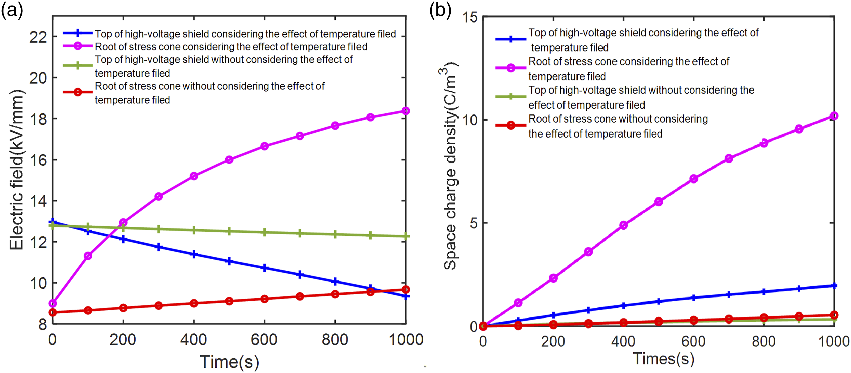
From the above, the stress cone root and the top of the high-voltage shield are considered the vulnerable points of the cable joint, which are prone to electric field distortion and lead to space charge accumulation, so they need to be paid more attention to. Figure 8(a) shows the change of the electric field modulus at two points with time whether the temperature field is considered or not. In 0–1000 s, considering the temperature field, the electric field at stress cone root increases from 8.99 kV/mm to 18.38 kV/mm, increasing by 2.04 times, and the electric field at the top of the high-voltage shield decreases from 12.97 kV/mm to 9.36 kV/mm, decreasing by 1.39 times. Additionally, without considering the temperature field, the electric field at stress cone root increases from 8.56 kV/mm to 9.68 kV/mm, an increase of 1.13 times, and the electric field at the top of the high-voltage shield decreases from 12.79 kV/mm to 12.27 kV/mm, a decrease of 1.04 times. It is not hard to find that the electric field at both two points changes gently with time when the temperature field is not considered.
Figure 8(b) shows the change of the space charge density at the stress cone root and the top of the high-voltage shield with time whether the temperature field is considered or not. The space charge at both two points have changed little without considering temperature field. Combined with Figure 8(a), it is evident that the electric field at the top of the high-voltage shield gradually decreases, while the space charge increases by 1.97 C/m3 within 1000 s in the basic model. Because the presence of an appropriate amount of homo-charge can reduce the electric field here and alleviate the electric field distortion. Whereas considering the temperature field, the electric field and space charge at the stress cone root have significantly increased. It is obvious that the actual temperature change in the cable joint makes the joint insulation face more severe challenges.
Conclusions
The space charge behavior in cable joints has been characterized using the bipolar charge transport model. The accumulation characteristics of space charge are analyzed through numerical simulation, and the effects of trap depth and temperature field on space charge behavior are studied. The conclusions are summarized as follows:
The trap depth based on the molecular chain displacement is larger than that of the basic model and is positively correlated with the electric field. The trap depth at the stress cone root and the top of the high-voltage shield is larger, reaching 1.107 eV and 1.056 eV respectively at 500 s, and the high-voltage shield root is smaller. Therefore, compared with the basic model, the deeper trap depth will limit and hinder the space charge transport leading to a large amount of charge accumulated at the interface.
The charge transport model without considering the temperature field accumulates less charge at the interface than the basic model, and the electric field at the stress cone root and the top of the high-voltage shield changes gently with time. Considering the temperature field, the space charge at the top of the high-voltage shield gradually increases, increasing by 1.97 C/m3 in 1000 s, and the electric field gradually decreases, decreasing by 3.61 kV/mm in 1000 s. Yet the space charge and the electric field at the stress cone root all increase significantly, increasing by 10.13 C/m3 and 9.39 kV/mm respectively in 1000 s. The temperature field makes the insulation at stress cone root face more severe challenges.
Footnotes
Declaration of conflicting interests
The author(s) declared no potential conflicts of interest with respect to the research, authorship, and/or publication of this article.
Funding
The author(s) disclosed receipt of the following financial support for the research, authorship, and/or publication of this article: This work was supported by Natural Science Foundation of Liaoning Province under Contract No. 2020-MS-214 and Program for Innovative Talents in University of Liaoning Province under the Grant LR2019047.