
Abstract
Micro-optics and micro-structures play important roles in the field of optics. A multi-step processing strategy with the combination of various processing technologies has been applied to fabricate micro-optics and micro-structures. However, the multi-step processing method is complex and expensive. In this work, a rapid CO2 laser processing technique is proposed to fabricate micro-optics and micro-structures on fused silica materials. First, high-power and short-pulse CO2 laser is used to achieve rapid prototyping of micro-optics and micro-structures with pre-designed geometry on fused silica. In this step, a maximum material removal rate of 1.53 mm3/min could be achieved with surface roughness better than 100 nm. Then, using the same CO2 laser source with reduced laser power density, the initially processed fused silica surface could be smoothed to improve the surface quality. By simulating the CO2 laser interaction with fused silica material, the formation mechanism of smooth surface is revealed, and the processing parameters for achieving smooth silica surface are proposed. The surface roughness of finally processed silica surface could reach 10.8 nm. Finally, as an application example of the processed two-step CO2 laser processing method, a micro-structure with special hexagonal shape on fused silica optics is successfully processed. The proposed rapid CO2 laser processing technique for the fabrication of micro-optics and micro-structures on fused silica materials can be realized with only one equipment, which can not only ensure the processing accuracy and efficiency but also reduce the processing cost.
Introduction
Micro-optics and micro-structures are widely used in optical communication, micro-opto-electro-mechanical systems, lab-on-a-chip devices sensor applications and other fields.1–3 Also, there are many kinds of micro-optics and micro-structures, such as microfluidic channels,4–6 micro-lens arrays,1,7,8 optical fiber,9,10 diffractive optics, 11 holographic structures 12 and laser-induced periodic surface structures (LIPSSs). 13 Compared with micro-optics and micro-structures made of polymers, those micro-optics and micro-structures made of glass have been widely and reliably used in harsh environments due to their stable thermal, chemical and physical properties.
High geometric accuracy, smooth surface, superior optical performance and high machining efficiency are usually required when fabricating micro-optics and micro-structures. 14 The common fabrication methods of micro-optics and micro-structures mainly include photolithography, 15 hot embossing,16,17 etching18,19 and electrochemical polishing. 20 Because of the low efficiency or poor surface quality of these processing techniques, they cannot be widely used to process micro-optics and micro-structures. However, the laser processing technique possesses great application potential in processing both metallic and non-metallic materials for its high processing efficiency and processing precision.21–23 There are three main methods to manufacture micro-optics and micro-structure based on laser processing technique: (a) Combination of laser and hot embossing or etching.5,14 This method effectively improved the efficiency of processing, but the combined process is complex and the equipment is expensive; (b) Combination of different lasers.4,7,24,25 Generally, this method is the combination of ultrafast laser and CO2 laser, where the ultrafast laser is used for rapid prototyping, while the CO2 laser is used for smoothing surface; (c) Laser direct writing.12,26 The laser used for direct writing includes ultrafast laser, 27 solid-state laser 28 and CO2 laser.12,26 In particular, ultrafast laser has gained interest in processing optical materials. However, compared with CO2 laser, the ultrafast laser and solid-state laser are so expensive. Furthermore, the surface processed by ultrafast laser and solid-state laser is rough, although their processing efficiency is very high. Therefore, it is necessary to develop a new technique, which can not only ensure the processing accuracy and efficiency but also reduce the processing cost.
With the development of laser technique, high-power and short-pulse CO2 laser can be generated directly. Laser pulses with peak power of 40 kW and pulse width of 250 ns can be generated by Q-switching technique. 29 The laser pulses with peak power of 200 W and pulse width of 10 μs can be generated by acousto-optic modulator (AOM). 12 By changing the parameters of CO2 laser, the two-step processing method for generating and smoothing micro-optics and micro-structures can be realized, respectively. When processing the micro-optics and micro-structures, the ultrafast laser can be replaced by high-power and short-pulse CO2 laser. Therefore, a rapid CO2 laser processing technique for fabrication of micro-optics and micro-structures on fused silica materials is proposed in this work, which can not only ensure the processing accuracy and efficiency but also reduce the processing cost.
Experiments and measurements
The experimental setup for CO2 laser processing of micro-optics and micro-structures on fused silica optics is shown in Figure 1. A pulsed CO2 laser source with a maximum output power of Pmax≈ 100 W is used. An external AOM is used for picking pulse and modulating rectangular pulse out of continuous wave (CW) laser radiation. The rectangular pulse width is larger than 1 μs. The focused CO2 laser moves in a 25 mm × 25 mm area under the control of galvanometer scanning system. The combined focusing lenses with focal length of 100 mm focus the diffracted laser beam onto the surface of the fused-silica optics. The focused beam has a radius of 45 μm at 1/e. The maximum moving velocity of the laser beam is 3 m/s. The galvanometer scanning system and focusing lens are installed on the Z stage, and the beam size can be changed by moving the z-axis. Furthermore, the X-Y motion stage enables the movement of fused-silica sample in X and Y directions.
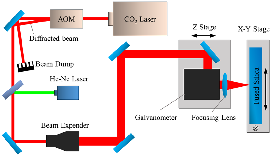
Experimental setup for CO2 laser processing of micro-optics and micro-structures on fused silica optics.
In addition, double-channel pulse generator is used in the control system to control the parameters of laser and AOM. The output CO2 laser pulse from the laser device is set to be continuous to simplify the experiment. By controlling the signal of AOM, laser pulses with different frequency, pulse width and power are obtained. The AOM enables accurate control of the peak power by adjusting the AOM voltage. Shorter laser pulses are obtained by providing a gating signal to the AOM, as illustrated in Figure 2(a). The peak power as a function of the AOM voltage of the AOM gating signal is shown in Figure 2(b).
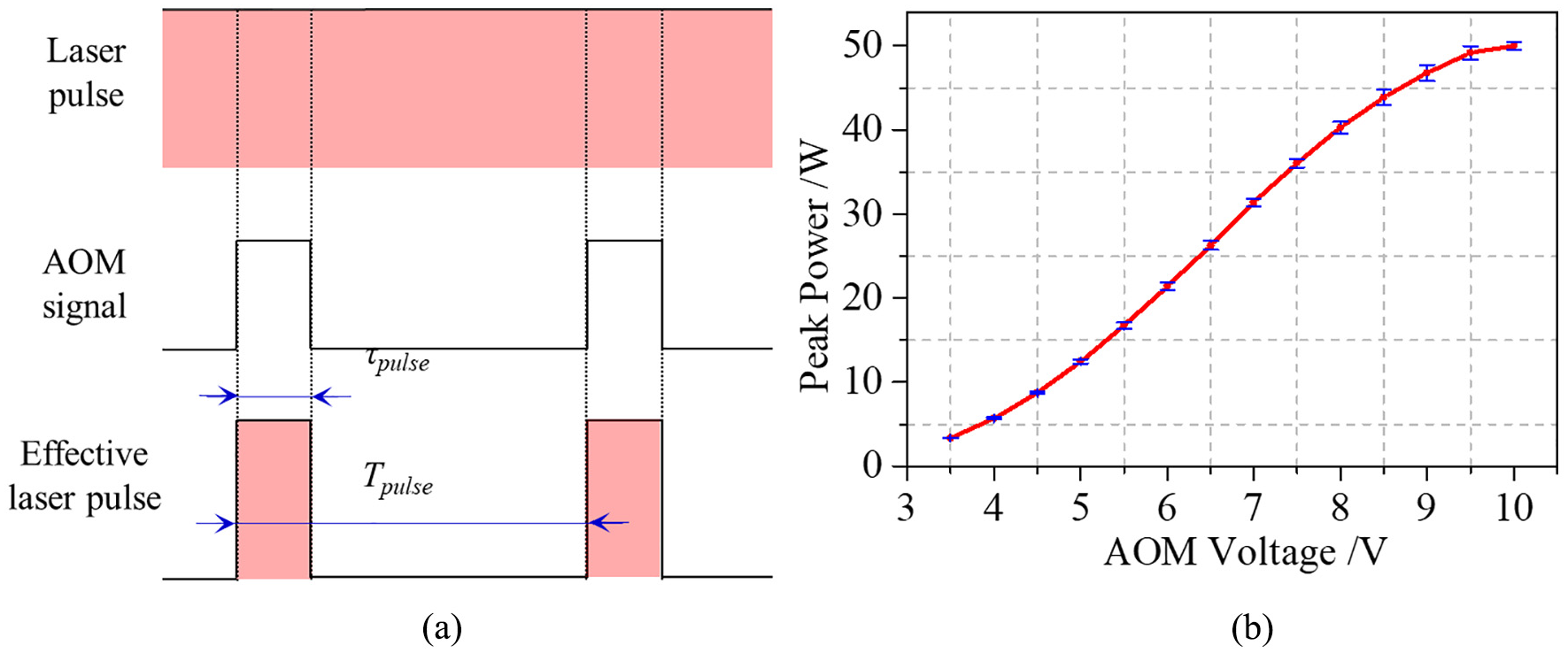
(a) Control of the width of laser pulses using AOM and (b) peak power on the workpiece as a function of the AOM voltage.
Laser energy is deposited on the surface of fused silica to form a processing region at high temperature. Figure 3 shows the schematic diagram of the CO2 laser processing of fused-silica optics. The focused laser beam with average laser power Pa, pulse width tp, frequency f and radius r0 moves across the surface with a scan velocity vs in a unidirectional scan strategy, which could result in the pulsed distance dx, track pitch dy, processed layer n and dx can be calculated by
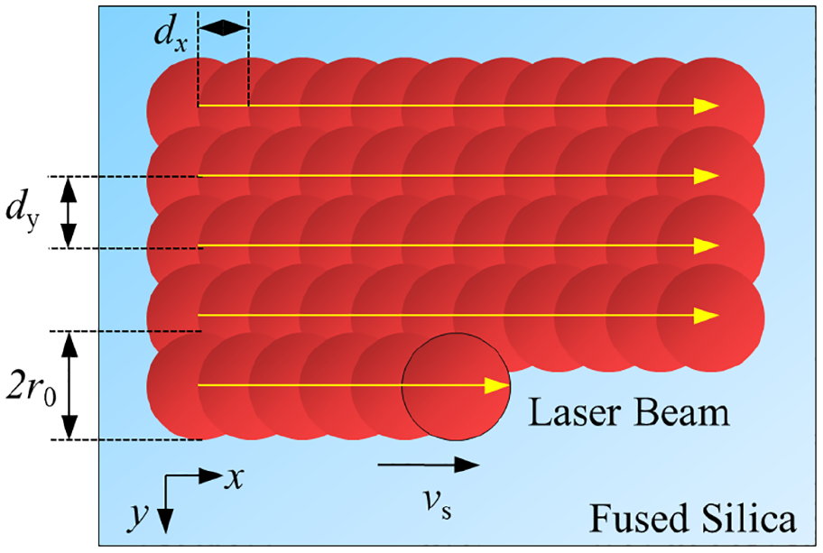
Schematic diagram of the CO2 laser processing of fused-silica optics.
The average material removal rate V of the processed area can be calculated by equation (2), to investigate the influence of processing parameters
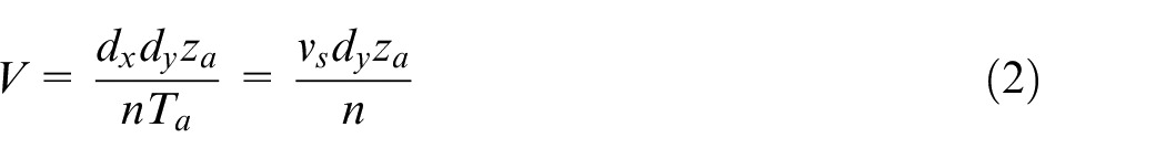
where Ta is the period of pulsed laser and za is the processed depth.
The samples used in this work are Corning 7980 fused silica. The surface morphological details of the processed surface on fused-silica optics are examined by white light interferometer and profilometer and observed by high-magnification optical microscope.
Results and discussion
In this work, the micro-optics and micro-structures on fused silica are mainly fabricated in two steps: rapid prototyping and surface smoothing. The two-step processing method is studied and the results are discussed in this section.
Rapid prototyping
In order to realize the processing of micro-optics and micro-structures on fused silica optics, the rapid prototyping of micro-optics and micro-structures is needed first. The high-power CO2 laser can be used to quickly remove the material on fused silica surface to achieve the pre-designed geometry of micro-optics and micro-structures. Many parameters are involved in the process of CO2 laser processing, so it is necessary to find appropriate parameters to achieve high material removal rate and good surface quality.
The experiment of surface ablating on the fused-silica is carried out to acquire the optimal parameter of rapid prototyping with focused CO2 laser. The laser parameters with a power of 50 W, frequency of 10 kHz and pulse width of 10 μs are used to process fused-silica optics. Meanwhile, pulse distance dx, track pitch dy and processing layer n are variable parameters. The curves of ablation depth as a function of pulse distance, track pitch and processing layer are shown in Figure 4. The results show that the ablation depth decreases exponentially with the increase of pulse distance and track pitch. The maximum ablation depth is 443 μm with corresponding parameters of dx = 4.5 μm, dy = 9 μm and n = 10. Besides, it can be seen in Figure 4(c) that the ablation depth increases linearly with the increase of processing layers. Also, the smaller the pulse distance is, the faster the ablation depth increases. This is because that smaller the pulse distance results in higher the laser overlap rate and higher the average energy density of the processing area. It can be seen that processing parameters corresponding to the material removal depth of single layer can be obtained. Material removal at different depths can be realized by changing the number of processing layers, which can be used in the rapid prototyping of micro-optics and micro-structures on fused silica.
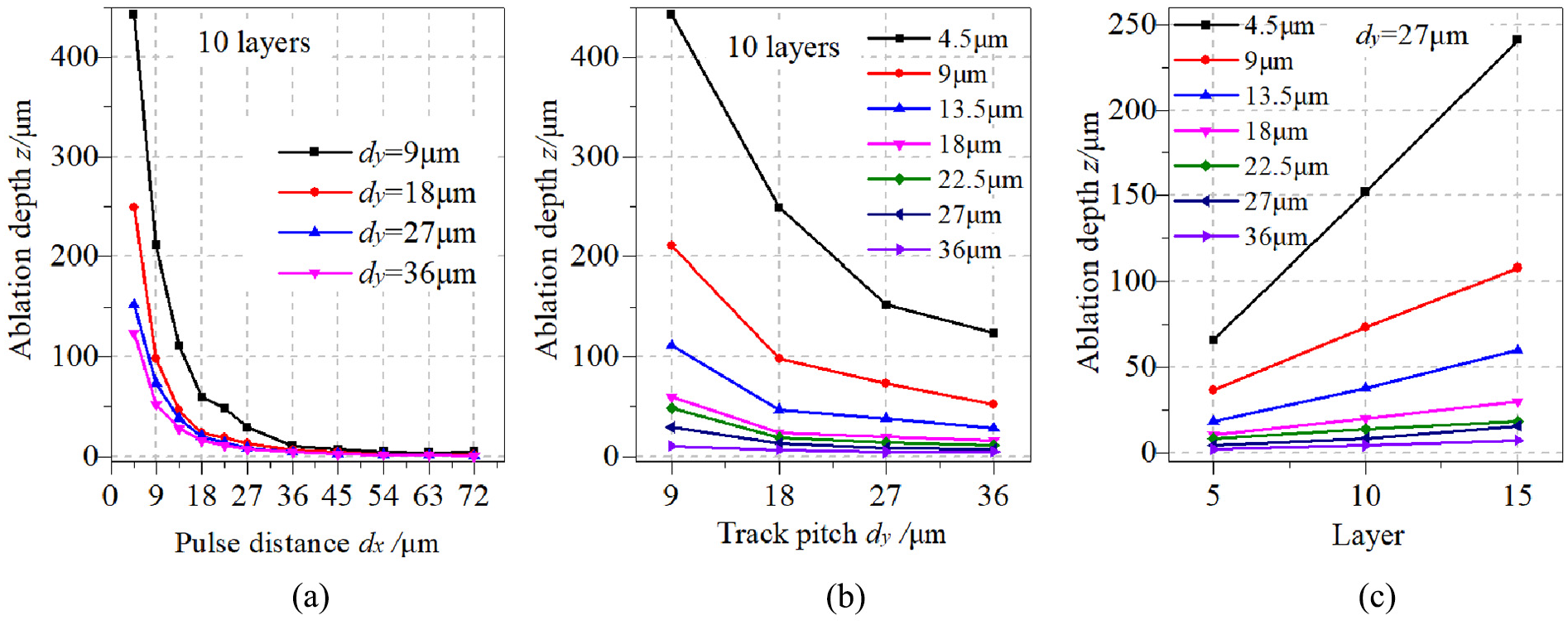
The curves of ablation depth for CO2 laser processing fused silica optics with power of 50 W, pulse width of 10 μs and frequency of 10 kHz. Ablation depth as a function of (a) pulse distance for processed layer n = 10, track pitch 9 μm < dy < 36 μm and pulse distance 4.5 μm < dy < 72 μm; (b) track pitch for processed layer n = 10, track pitch 9 μm < dy < 36 μm and pulse distance 4.5 μm < dy < 36 μm; (c) processed layer for track pitch dy = 36 μm, processed layer 5 < n < 10 and pulse distance 4.5 μm < dy < 36 μm.
Removal rate is an important index of processing efficiency in laser processing, which is considered in this work. In order to reduce the effects of power fluctuation, 10 processing layers of the removal area are carried out in the experiment. Therefore, the parameters with power of 50 W, frequency of 10 kHz and pulse width of 10 μs are chosen and kept constant for the following investigations. For this experiment, regions with the dimensions of 2.5 mm × 2.5 mm are processed. The evolution curves of surface morphology for different pulse distances dx and track pitches dy are shown in Figure 5. And the material removal rate V can be calculated with equation (2). The results of material removal rate for different pulse distances dx and track pitches dy are shown in Figure 6. It is shown that the material removal rate increases rapidly with the decrease in pulse distance, while the track pitch has very limited effect on the removal rate. It is because the smaller the pulse distance is, the higher the laser overlap rate is, and the higher the temperature of the surface will be after the laser processing. Therefore, it needs less energy to heat the material to the ablation state in the next laser pulse processing, and more materials can be removed. On the contrary, the time of processing a line is longer in a unidirectional scan strategy. In this experiment, when the pulse distance dx = 4.5 μm (scan velocity vs = 45 mm/s, scan distance is 2.5 mm), the time of scanning a line is 55.6 ms. However, it takes only 20 ms for the surface temperature of fused silica to decrease from 2500 K to below 1000 K with the condition of room temperature cooling. 30 The temperature of the material surface is lower when the second scanning is carried out due to enough cooling time.
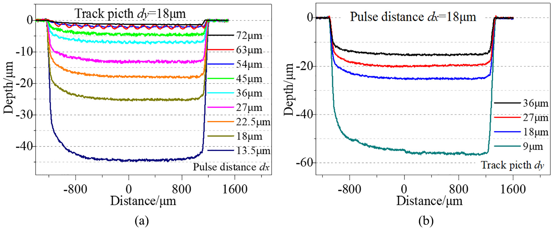
The evolution curves of surface morphology for (a) pulse distance dx increases from 13.5 to 72 μm at track pitch dy = 18 μm and (b) track pitch dy increases from 9 to 36 μm at pulse distance dx = 18 μm.
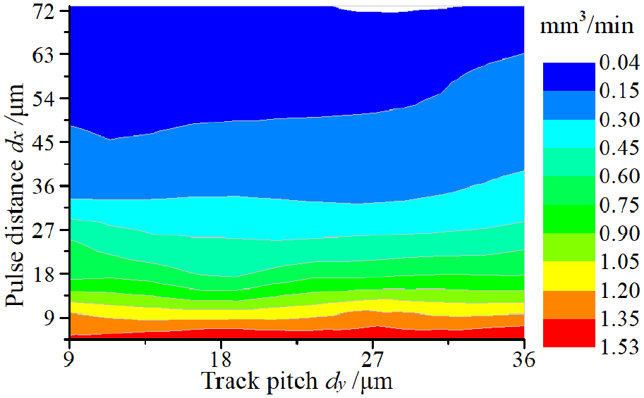
Material removal rate V for different pulse distances dx and track pitches dy.
As shown in Figure 6, the maximum removal rate of 1.53 mm3/min can be realized in this work. Therefore, the surface quality can be improved by changing the track pitch with the required removal rate in the rapid prototyping process.
In order to obtain better surface quality, the surface roughness of optics after processing with different parameters is measured. The surface roughness as a function of pulse distances dx at different processing layers with track pitches dy = 9 μm and 18 μm are shown in Figure 7. Generally, the surface roughness decreases with the increase in pulse distance. However, some singular points appear at special pulse distance. At this time, the surface roughness increases rapidly and the surface quality deteriorates seriously. For instance, when the pulse distance dx increases from 36 to 45 μm at 10 processing layers with track pitch dy = 9 μm, the roughness increases from 65 to 219 nm. Similarly, when the track pitch dy = 18 μm, the surface roughness value is very high at the pulse distances of dx = 36 μm and dx = 63 μm. It is observed that the surface processed by the singular point parameters generates periodic structures, as shown in the inset of Figure 6. Therefore, the parameters corresponding to singular points should be avoided in processing process. The processing parameters of pulse distance dx = 36 μm and dx = 22.5 μm at track pitch dy = 9 μm and pulse distance dx = 27 μm and 45 μm at track pitch dy = 18 μm in this work should be preferred. Thus, the processed surface roughness better than 100 nm can be achieved.
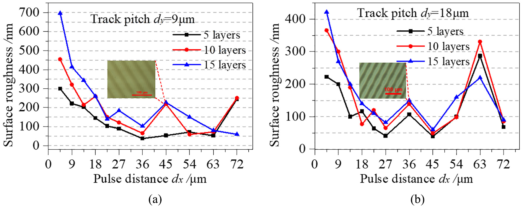
Surface roughness as a function of pulse distances dx at different processed layers with (a) track pitch dy = 9 μm and (b) track pitch dy = 18 μm.
Surface smoothing
The maximum power density is 1 MW/cm2 in this experiment, which exceeds the ablation threshold of fused silica.31,32 However, the surface smoothing can be realized by the melting flow of the material on the surface. Therefore, it is necessary to reduce the laser power density to smooth surface of the optics. In this experiment, the defocused beam is used to smooth the surface of fused silica optics. The surface roughness of applied fused silica sample is about 250 nm. A laser source with power of 50 W, frequency of 1 kHz, pulse width of 200 μs and processing time of 0.6 s is used to process fused silica optics. The processed surfaces of fused silica optics at different defocusing distances are shown in Figure 8. The initial surface roughness is 174 nm. The roughness is reduced to 147 nm with the defocusing distance of 11.5 mm, while the roughness is reduced to 78 nm with the defocusing distance of 10.5 mm. With the decrease in defocusing distance, the quality of processed surface becomes better. When the defocusing distance is less than 10.5 mm, a smooth surface is produced. It is because the smaller the defocus distance is, the smaller the spot diameter is, and the higher the energy density is. Temperature of the surface will be high under this condition and the melting flow generated on the surface forms a smooth surface. However, when the energy density is too high, the material removal would occur on the material surface. As shown in the last figure of Figure 8, a Gaussian-like pit with a width of 400 μm and a depth of 18 μm is formed. Therefore, the smooth surface can be processed with the defocusing distance of 9.5 mm, and the material removal can be avoided by controlling the laser dwell time.
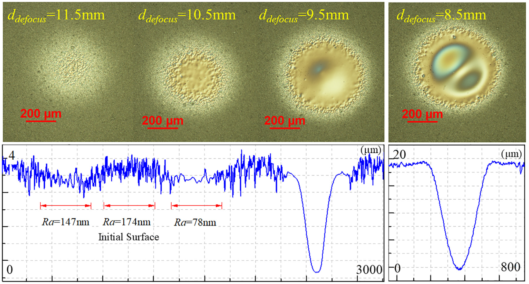
The processing surfaces of fused silica optics at different defocusing distances with the power of 50 W, frequency of 1 kHz, pulse width of 200 μs and processing time of 0.6 s.
The effect of laser dwell time on surface smoothness of fused silica at defocusing distance of 9.5 mm is investigated, and the results are shown in Figure 9. When the laser dwell time is less than 0.4 s, surface roughness of processed surface is similar to the initial surface due to low surface temperature and weak melting flow. With the increase in laser dwell time, the melting flow rate of the surface material increases, and the surface becomes smooth gradually. The surface roughness decreases from 168 to 73.6 nm at the laser dwell time of 0.4 s. When the laser dwell time is 0.5 s, the temperature of laser processing center is higher. A large temperature gradient is formed from the center to the edge of processing area, which results from the Marangoni effect. 33 Thus, the material in the central area moves to the edge, forming a pit. When the laser dwell time is 0.6 s, the surface temperature is higher than the ablation temperature of fused silica and consequently a deeper pit is formed.
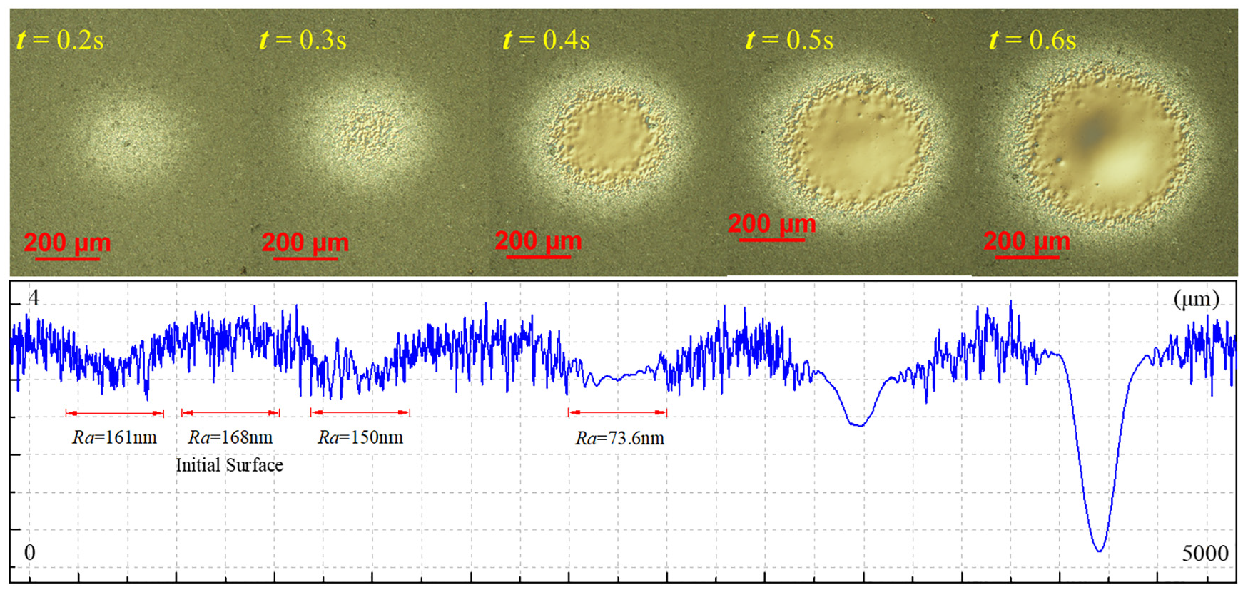
The processing surfaces of fused silica optics at processing time from 0.2 to 0.6 s with the power of 50 W, frequency of 1 kHz, pulse width of 200 μs and defocusing distance of 9.5 mm.
It is worth noting that a pit with a depth of 200 nm is formed even if the material does not melt and be ablated at the laser dwell time of 0.2 s. It is due to the modification of the material in the laser processing area, which would incur in the increase of the fictive temperature, the decrease of the density and the shrinkage of the volume.12,34
In order to reveal the smoothing mechanism of fused silica surface, a multiphysics-field model based on the interaction between CO2 laser and material is built, as shown in Figure 10. The interaction between laser and fused silica is a complex process involving phase transformation. 30 Fused silica has high absorption coefficient to CO2 laser at 10.6 μm wavelength, so the interaction between CO2 laser and fused silica is primarily a thermal process. When the temperature rises from 300 to 2000 K, the absorption depth of fused silica to CO2 laser decreases from 40 to 4 μm. Therefore, the heat absorbed by the fused silica concentrates on the surface, and the surface temperature could reach a molten state, which would rapidly smooth the surface of fused silica. The process of thermal transfer can be expressed as
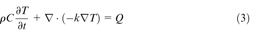
where ρ is the density of material (2.20 g/cm3), C is the specific heat capacity under constant pressure, T is the temperature, k is the thermal conductivity and Q is the incident heat source. The incident heat source Q is calculated by

where r0 is the radius at 1/e of a Gaussian laser profile, R is the Fresnel reflection coefficient (0.15) and α is the absorption coefficient.
As a kind of viscoelastic material, fused silica could be considered as viscous fluid when the temperature increases to its melting point. The distributions of velocity field and pressure field can be described by momentum balance equation (N-S)


where μ(T) is the dynamic viscosity a function of temperature T, u is the velocity vector, ρ is the material density, p is the pressure and Fv is the driving force of fluid flow.
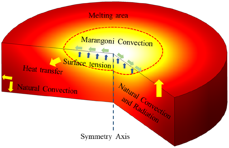
Schematic of multi-physics process of CO2 laser polishing of fused silica.
In order to simulate CO2 laser interaction with rough fused silica, the fused silica surface is set as a sinusoidal structure with period of 2 μm, amplitude of 800 nm and surface roughness Ra of 255 nm. The laser with power of 50 W, frequency of 1 kHz and pulse width of 200 μs are used to process fused silica optics. The laser beam is nearly Gaussian distribution with diameter of 0.7 mm at 1/e. Driven by surface tension, Marangoni effect, the surface material undergoes melting flow. The surface morphology smoothed by CO2 laser at different processing time is shown in Figure 11.
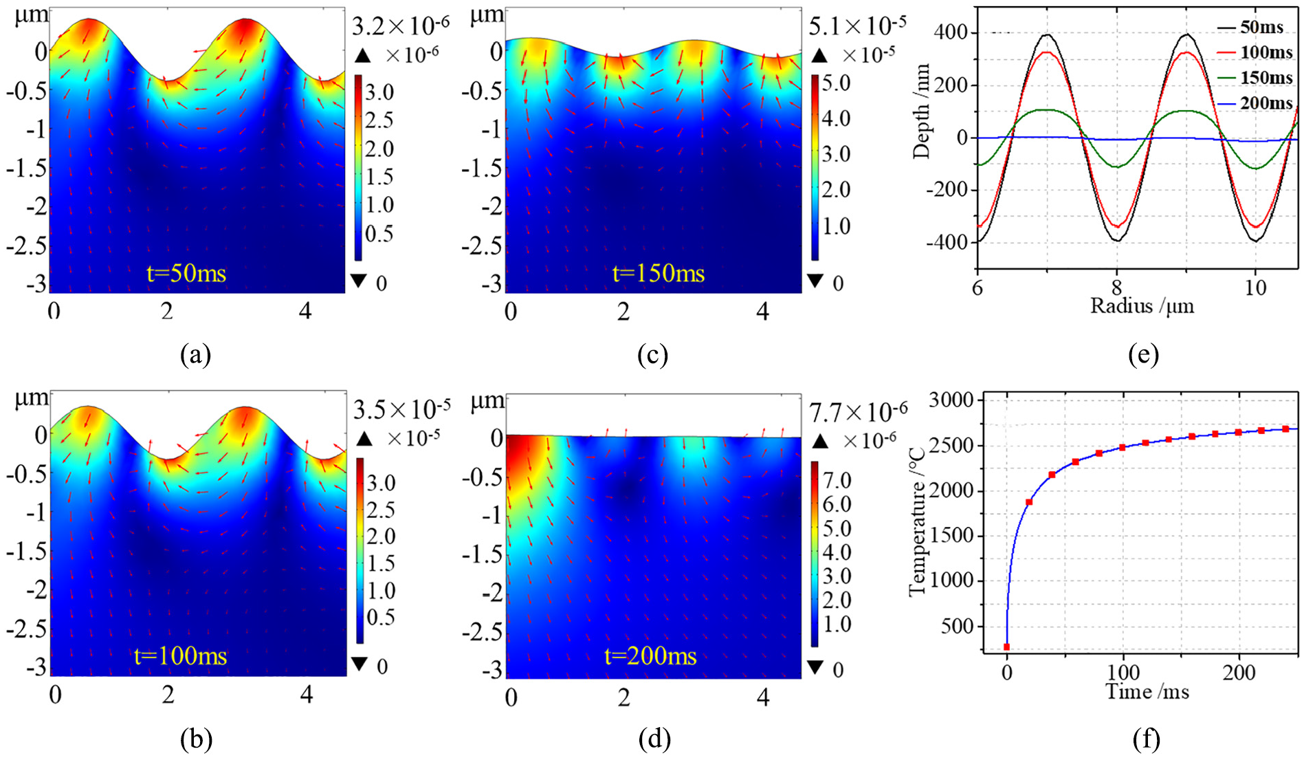
The simulated flow fields of fused silica with CO2 laser processing times of (a) 50 ms, (b) 50 ms, (c) 150 ms and (d) 50 ms. (e) Evolution of the surface morphology during surface smoothing process and (f) curve of maximum temperature during surface smoothing process.
The maximum temperature increases exponentially with the increase in laser processing time. At the beginning, the laser energy is used to heat the material, because the substrate temperature of the material is 273 K. When the laser processing time reaches 26 ms, the maximum temperature of the material surface is 2000 K, and the material begins to melt. According to the flow fields shown in Figure 11(a)–(d), it can be analyzed that the material at the peak of morphology flows out to the valley bottom, filling the structure and making the material surface smooth. Figure 11(e) shows the evolution of the surface morphology during the surface smoothing process. When the laser processing time reaches 200 ms, the amplitude of the surface morphology decreases to 10 nm. In the subsequent laser processing, the smooth surface could be achieved. Figure 11(f) shows that the surface temperature reaches 2700 K at the laser processing time of 200 ms. And the material would be ablated if the laser continues to work.
It can be seen from above analysis that the surface becomes very smooth at laser processing time of 200 ms. The surface would continue to change with the increase in laser processing time, as shown in Figure 12. The distribution of flow field shows that the material migrates from the center to the edge in the laser processing area. And the maximum migration velocity appears at the position of the maximum temperature gradient. Finally, a pit in the center with bulge at the edge is formed, as shown in Figure 12(d). Obviously, it deteriorates the surface quality of fused silica optics. Therefore, the laser dwell time should be controlled to avoid secondary bulge on the surface.
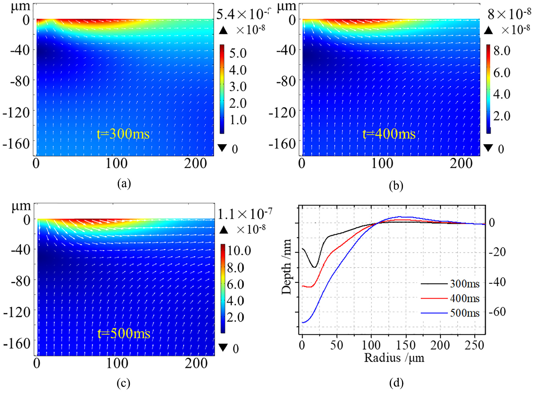
The simulated flow fields of fused silica with CO2 laser processing times of (a) 300 ms, (b) 400 ms and (c) 500 ms. (d) Evolution of the surface morphology driven by Marangoni effect.
The simulation results reveal the smoothing mechanism of fused silica surface processed by CO2 laser. It shows that the processed surface quality would be deteriorated with long laser dwell time. In addition, surface temperature of materials could reach 2700 K at the dwell time of 500 ms, and the materials would be ablated. However, the material ablation was not considered in this simulation. Therefore, the pit depth of the simulation results in Figure 12 was less than that of the experimental results in Figure 9.
The results show that the surface of fused silica is smooth at the defocusing distance of 9.5 mm. The laser with power of 50 W, frequency of 1 kHz and pulse width of 200 μs are used to process fused silica optics. And the light transmittance of the optics with smooth surface is tested, which is shown in Figure 13. Figure 13(a) shows the fused silica sample used in experiment, with the size of 50 mm × 50 mm × 5 mm. Figure 13(b) is a partial view of the light transmittance experiment, in which C is the smooth surface area and B is the rough surface area before CO2 laser smoothing. The image under the optics in area C can be clearly observed, while the image in area B is blurred. The surface roughness of areas B and C are measured, as shown in Figure 13(c) and (d). The results show that the surface roughness of the surface can be reduced from 239 to 10.6 nm after CO2 laser smoothing. Thus, a smooth surface on fused silica material is processed with defocused CO2 laser.
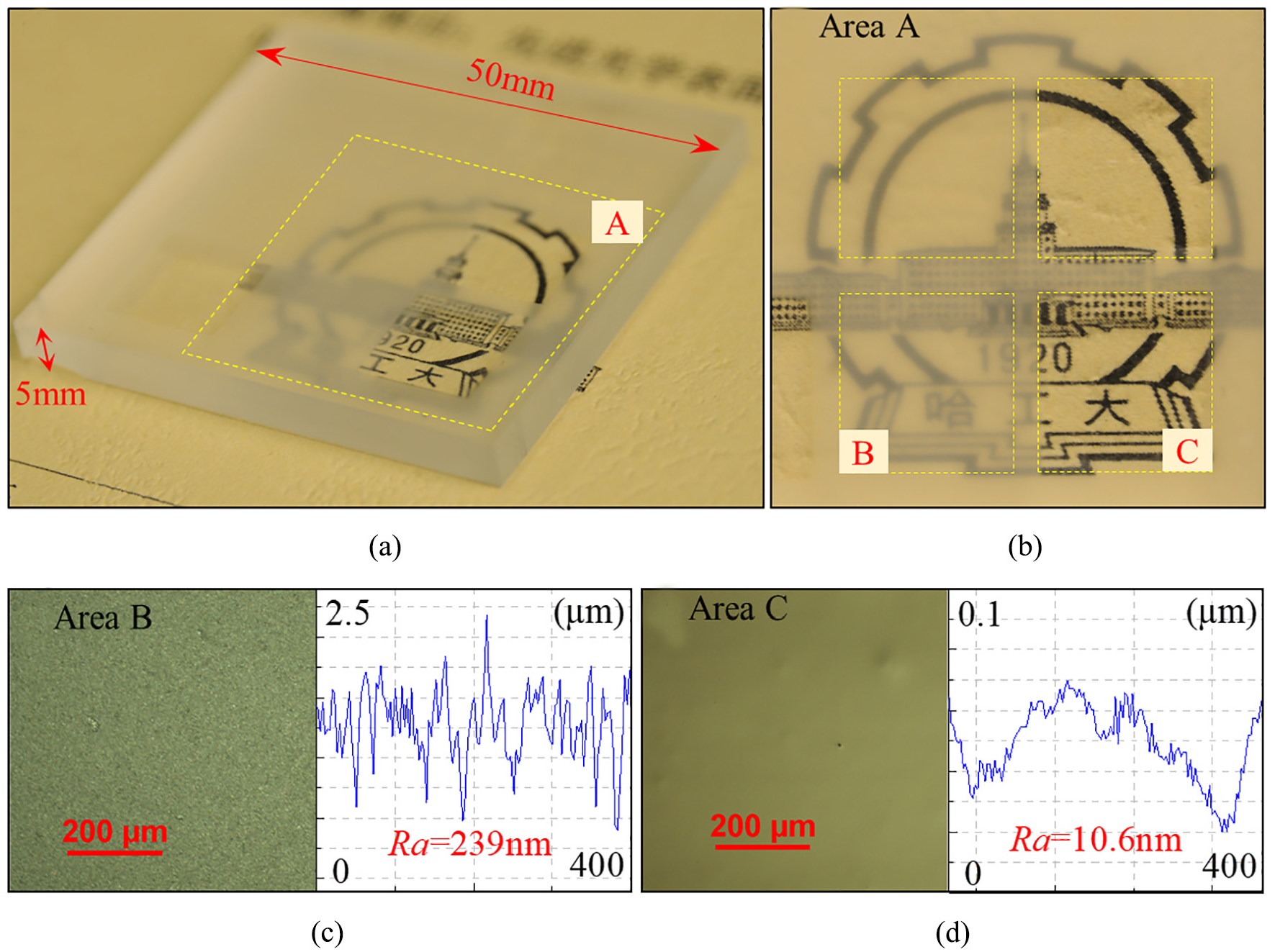
Experimental results of surface smoothness on fused silica optics: (a) rough fused silica sample before CO2 laser smoothing, (b) partial view of the light transmittance result, (c) optical micrograph and roughness of area B and (d) optical micrograph and roughness of area C.
Application
Using the experimental setup, a special hexagonal micro-structure on the surface of fused silica optics is processed, which is shown in Figure 14. The regular hexagon micro-structure has a side length of 0.75 mm and a depth of 415 μm. The focused laser beam with parameters of pulse distance dx = 36 μm and track pitch dy = 9 μm is used to achieve rapid prototyping, and the defocused laser beam with parameters of pulse distance dx = 6.8 μm and track pitch dy = 135 μm is used to smooth surface. It consumes 69.48 s to process the hexagonal micro-structure with the proposed two-step processing method. The results show that the rapid CO2 laser processing technique has advantages of high processing efficiency and low cost. Therefore, it has application prospect in processing micro-optics and micro-structures on fused silica optics.
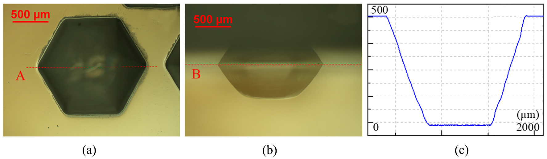
The hexagonal micro-structure processed on the surface of fused silica optics: (a) front view observed by optical microscope; (b) section view observed by optical microscope through side polished optics, where line B is the surface; and (c) surface profile along line A in (a).
Conclusion
A rapid CO2 laser processing technique for the fabrication of micro-optics and micro-structures on fused silica materials is proposed. The processing flow includes two steps: rapid prototyping and surface smoothing.
In the step of rapid prototyping, high-power and short-pulse CO2 laser is used to quickly realize the pre-designed geometry. The results indicate that the processed surface roughness better than 100 nm could be achieved with the preferred processing parameters.
In the step of surface smoothing, by using the same CO2 laser source with lower laser power density, the effect of melting flow could work and the initially processed surface could be smoothed to improve the surface quality and the surface roughness of 10.8 nm could be reached.
A multiphysics-field model based on the interaction between CO2 laser and fused silica material is built to reveal the surface smoothing mechanism: the thermal capillary force (Marangoni effect) drives the melting flow of the material to smooth the surface.
Special hexagonal micro-structure (side length of 1 mm and depth of 415 μm) on fused silica material is successfully processed using the optimized processing parameters.
The proposed rapid CO2 laser processing technique can be realized based on only one laser equipment, which can not only ensure the processing accuracy and efficiency but also reduce the processing cost. Hence, it possesses a great potential application value that it could be applied as an alternative processing method for the rapid processing of micro-optics and micro-structures.
Footnotes
Declaration of conflicting interests
The author(s) declared no potential conflicts of interest with respect to the research, authorship, and/or publication of this article.
Funding
The author(s) disclosed receipt of the following financial support for the research, authorship, and/or publication of this article: This work was supported by the National Natural Science Foundation of China (Grant Nos 51775147 and 51705105), Science Challenge Project (Grant No. TZ2016006-0503-01), Young Elite Scientists Sponsorship Program by CAST (No. 2018QNRC001) and Self-Planned Task (Grant Nos SKLRS201718A and SKLRS201803B) of State Key Laboratory of Robotics and System (HIT).