
Abstract
In the present study, an atomic force microscopy tip-based nanomilling approach is used to fabricate nanochannels on a poly(methyl methacrylate) surface. A silicon atomic force microscopy tip is employed for all the scratching tests. Results show that the material removal state is obviously different from the conventional single scratch process. Chips can be formed during the nanomilling operations and the height of the material pile-up can thus be reduced. The generation of chips may be attributed to the changes of the cutting angle and the feed value during one complete rotation of the scratching process. Moreover, this particular implementation of the atomic force microscopy scratching technique is proved to form nanochannels, following a two-step process during one complete rotation: the first half cycle forms the outer profile and the second half cycle generates the inner profile and increases the machined depth. The scratching trajectories to obtain the outer profile and inner profile are studied in detail. Finally, the change of machined depth in one scratching cycle for the nanomilling process is also investigated. It is anticipated that this method could be employed to fabricate nanochannel used in nanofluidic applications.
Introduction
Nowadays, with the rapid development of nanotechnology-based applications, micro- and nanostructures-based sensors have been widely applied in the experimental research fields of chemistry,1–3 biology,4–6 and especially for nanofluidics. Among these, a nanofluidic-based label-free detection technique shows great potential in healthcare, medicine, and life sciences. 7 The detection of the ionic conduction of the nanochannels is used in this approach to investigate reaction kinetics of some chemical or biological reactions. Channels with nanoscale features are key parts in this method. How to fabricate size controllable and good quality nanochannels used in the label-free detection technique is still a difficult issue. Although some scholars have fabricated nanochannels-based sensors using focused ion beam, 8 electron beam, 9 and nanoimprint lithography 10 successfully, the complexity and/or cost of these methods greatly impede the fabrication of nanochannels.
When the atomic force microscope (AFM) was invented in 1986 by Binnig et al., 11 it was first considered as a profilometer on a nanoscale. In the last two decades, more and more researchers utilized the AFM as a nanomachining tools to fabricate nanostructures. This is due to the AFM due to the characteristics of simple operation, low cost, high machining precision, and atmospheric environmental requirement. 12 Among these AFM tip-based nanofabrication methods, nanomechanical machining has been proved to be most feasible and easiest approach to achieve nanostructures. This method has been employed to fabricate nanodots, 13 nanochannels, 14 two-dimensional (2D) and even three-dimensional (3D) nanostructures 15 on various materials such as metal, 16 polymer, 17 and semiconductor. 18 For the metal and semiconductor materials, a relatively large normal load is needed to achieve nanostructures with a desired machined depth. Thus, the diamond AFM tip is usually selected to scratch on such materials to avoid or reduce tip wear. However, due to the relatively large size of the diamond AFM tip, it is difficult to obtain nanostructures with a width less than 100 nm.14,16 Furthermore, a serious tip wear can occur when scratching on semiconductor materials even using a diamond tip due to the large hardness of this type of material. 19 This leads to difficulties when considering large-scale and long-term fabrication. Therefore, polymer materials have been more and more widely selected as the substrate in the AFM tip-based nanomechanical machining approach because of their good machinability and lower hardness resulting in reduction of the wear rate of the AFM tip. A silicon tip with small radius is usually chosen to scratch on a polymer material. 20 However, due to the viscoelastic behavior of polymers, the material is mainly removed in the form of material accumulation and the accumulation of surface pile-up on both sides of the groove. 17 This large pile-up can lead to reduced bonding and nanochannels clogging during the following chip bonding process for the nanofluidic application, which results in the failure of preparation of the naonfluidic chip. In addition, the width of the nanochannel machined by single-pass scratching process is dependent on the geometry of the AFM tip. In this case, it is difficult to achieve the nanochannels with both controllable width and depth. Therefore, Zhang and Dong 21 and Gozen and Ozdoganlar 22 proposed a rotating-tip-based mechanical nanomachining technique, named nanomilling, to fabricate size controllable nanochannels. The AFM tip or the sample is rotated at high speeds combined with feeding motion of the sample to remove material. The amplitude of the rotary motion is used to control the width of the machined groove. Moreover, from their works, it was indicated that shearing is the dominant material removal mechanism to generate chips in the nanomilling machining process due to the relatively high machining speed. However, in their studies, either the tip directly attached onto the piezoelectric 22 or an ultrasonic z vibration of the sample 21 is used to increase the stiffness of the system, which results in the fabrication depth regulated by the relative displacement between the tip and the sample. The nanomilling process described in their studies is similar to the traditional milling process, which may lead to inconsistent machined depth along the scratching direction when the sample surface is tilt. Park et al. 23 compared the AFM topographies, depth profile, and force measurements with and without z vibration. However, only V-shaped nanochannels could be obtained in their study. Moreover, when the feedback loop of the AFM is still working during the scratching process, the tip also cuts the material in the second half scratching cycle of the rotation scratching process, which cannot occur in the traditional milling process. This will have large influence on the machined depth and the quality of the achieved nanochannel. No previous works focusing on the material removal state based on the combined effect of the cutting tool geometry and scratching trajectory during one revolution using this nanomilling approach are found up to now.
Therefore, in the present study, a modified AFM system with a high precision rotary stage is employed to machine nanochannels on a poly(methyl methacrylate) (PMMA) surface with a silicon tip using the nanomilling approach. The end of the groove is measured and investigated by simulation of the probe trajectory for one cross-section of the AFM tip. The tip–sample interaction and the material removal during one whole rotation of the scratching process are also studied.
Methodology
Nanomilling set-up and procedure
Figure 1(a) shows the schematic of the modified AFM tip-based nanomilling system, including a commercial AFM (Dimension 3100; Veeco Inc., USA), a 2D precision vibration platform (P-363.2CD; PI, Company, Germany), and a 3D high precision positioning stage (P-517.3CD; PI). The optical lever system of the AFM is employed to detect the deformation of the cantilever and the piezoceramics tube (PZT) is used to adjust the position of the tip to keep the deformation of the cantilever constant and thus to maintain the normal load applied on the sample surface by the AFM tip constant. The 2D precision vibration platform is utilized to generate a rotary motion in the horizontal plane. The resolution of this vibration platform along both x and y axes is 0.1 nm. The original stage of the AFM system is replaced by the 3D closed-loop, high precision positioning stage, which is used to conduct a uniform linear motion in the x-y plane with respect to the rotary motion of the 2D precision vibration platform. The motion ranges and resolutions of this stage in x, y, and z directions are 100 μm ± 5 nm, 100 μm ± 5 nm, and 20 μm ± 2 nm, respectively. As mentioned above, this precision stage only moves along the x and y directions to achieve the feed motion. Thus, the displacement in the z direction of this stage is set to zero during the whole scratching process. The combination of the rotary motion and linear motion of both high precision stages is derived as the relative motion between the sample and the AFM tip, which is shown in Figure 1(b). The rotary motion of the sample is denoted as t, and the linear motion is expressed as f. Similar as the tradition milling process, the uncut chip thickness is changing all the time during the machining process due to the rotary motion. Considering the load-constant machining mode of the AFM tip-based machining, the machined depth in one cycle should be changed. This should be due to the constant normal load applied by the tip as a result of the influence of the AFM feedback loop, which is specific to such an AFM-based implementation. Also, in order to maintain a constant normal force applied by the tip, the PZT of the AFM system should be driven up and down in the z direction to keep the deformation of the tip unchanged. This movement of the PZT is denoted as p in Figure 1(b).
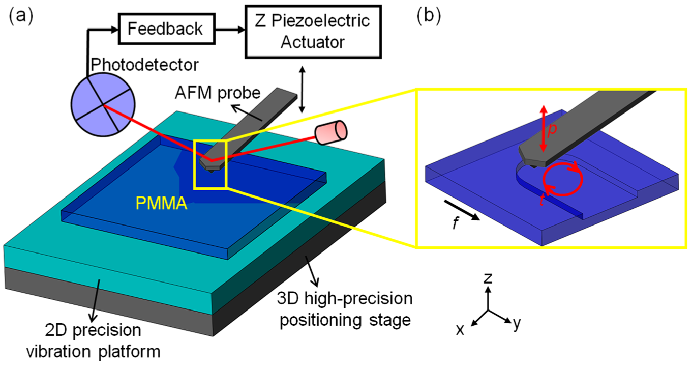
(a) Schematic of the nanomachining set-up and (b) relative movement between the AFM tip and the sample.
A silicon tip (Tap300-G; BudgetSensors Company, Bulgaria) is employed for all nanomachining operations. The cantilever for this kind of tip is also made of silicon with a normal spring constant of 49.6 N/m. The geometry of this tip is quadrangular pyramid with a radius less than 10 nm which is specified by the manufacturer.Figure 2(a) shows the scanning electron microscope (SEM) image of the tip. The mounted angle of the AFM probe on the AFM head is 12° in this study. Thus, the 3D geometry of this AFM tip can be obtained in a Cartesian coordinate system aligned with the surface of the sample, as shown in Figure 2(b). The four edges of the tip are denoted as OA, OB, OC, and OD. The corresponding cross-sections of the tip with the height of 10, 50, and 100 nm are shown in Figure 2(c). Points A′, B′, C′, and D′ in Figure 2(c) represent the projection points of A, B, C, and D in Figure 2(b), respectively. It can be observed from Figure 2(c) that the cross-section of the tip becomes closer to point A′ with the height decreasing due to the inclination angle of the AFM tip. The sample used in the present study is a PMMA sheet, purchased from Mitsubishi Rayon, Japan. The sample surface used in the machining process is provided by the manufacturer without any subsequent processing. The roughness of the sample surface is less than 2 nm, which is obtained by scanning a 50 μm × 50 μm area of the sample with a new silicon tip using tapping mode.
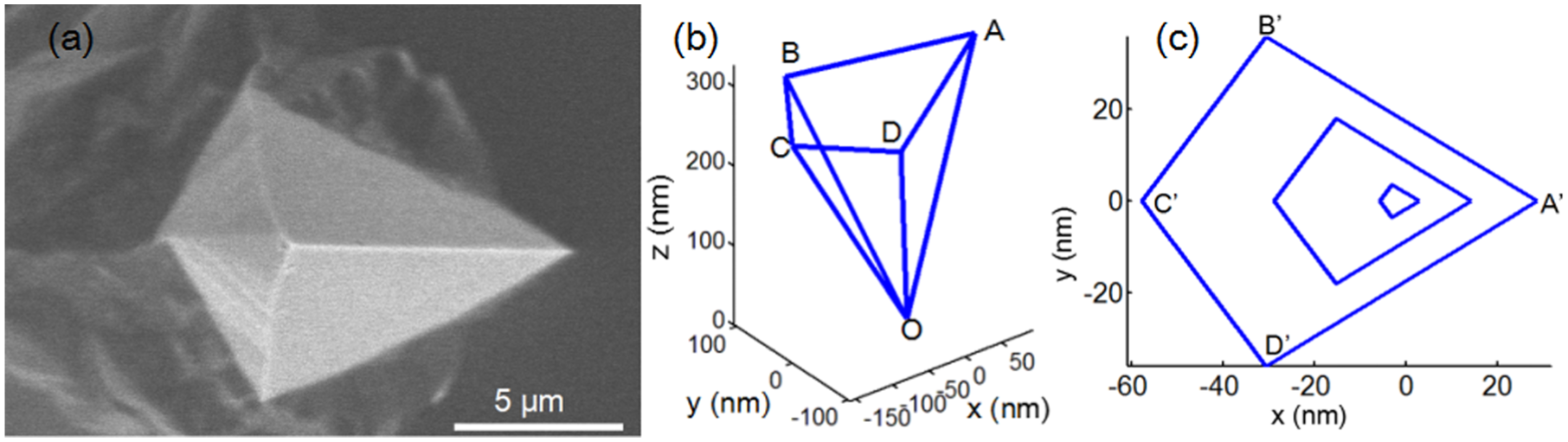
(a) SEM image of the silicon AFM tip. (b) Schematic of the tip in Cartesian coordinate system and (c) corresponding cross-sections of the tip with the height of 10, 50, and 100 nm.
Based on this nanomilling system, the procedure of machining the nanochannels is described as follows:
The AFM tip is controlled to approach the sample surface with a pre-set normal load. As mentioned above, this normal load is kept constant during the scratching process.
The 2D precision vibration platform is driven to conduct a rotary motion with a pre-set amplitude and frequency. The 3D high precision positioning stage is controlled to carry out a linear motion perpendicular to the probe cantilever at the same time. In order to study the cutting state of the nanomilling process, the AFM tip is lifted up when the 3D high precision stage nearly reaches the pre-set ending position. This can prevent the tip keeping machining at the end of the groove.
After one nanochannel is fabricated, the machining position along the x-axis is changed by the 3D high precision positioning stage. Another nanochannel parallel to the previous groove can be then fabricated. After all scratching processes, the machined grooves are scanned by the AFM tip directly without any cleaning operation to observe the accumulated materials on both sides of the grooves.
Characterization of the rotary trajectory
The 2D precision vibration platform is a critical component of the developed AFM-based nanomilling set-up to conduct rotary motion during machining. Thus, preliminary scratching tests are conducted to characterize its motions under various voltage values input. A multifunction data acquisition card (NI USB-6259; NI Company, USA) is employed to input two sinusoidal voltage signals with a phase difference of 90° to the two channels of the 2D precision vibration platform. The amplitude and frequency of the sinusoidal voltage signals for both x and y directions are controlled to be identical. This characterization procedure is performed as follows. The AFM tip approaches the sample at a given normal load and the 2D precision vibration platform is controlled to rotate with a pre-set amplitude and frequency. The 3D high precision positioning stage remains stationary. The AFM tip is then lifted up. After the scratching process, a new silicon tip is used to obtain the profile of the machined circular grooves using tapping mode. In this study, the voltage signals are chosen as 0.5, 1, 2, 3, 4, and 5 V, and the frequency is set as 10 Hz. The normal load used in these tests is selected as 2.9 μN. Figure 3 shows the circular grooves machined with various driving voltage values, and the relationship between the amplitude of the rotary motion and the voltage values. From Figure 3(d), it can be observed that the amplitude of the rotary motion increases linearly with the increase in the voltage value. This indicates that the nanomilling process utilized in this study can be used to fabricate nanochannel with controllable width.
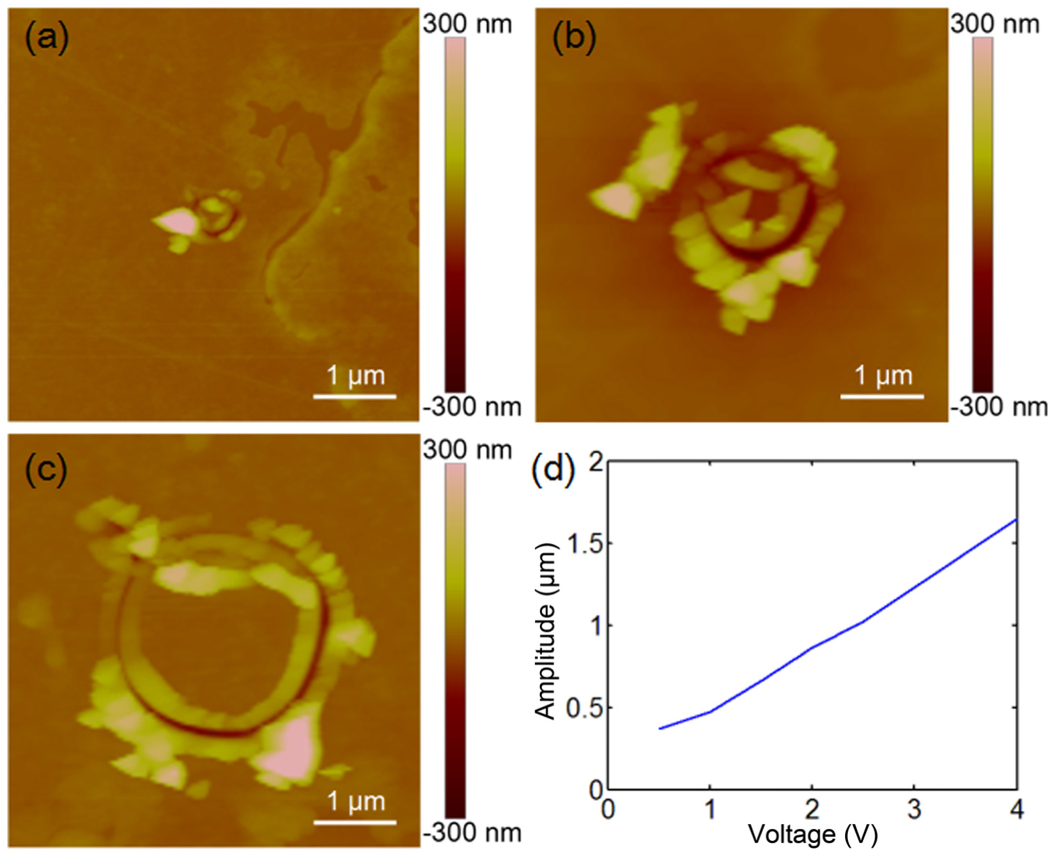
Circle grooves machined with various driving voltage values of 1 V (a), 3 V (b), and 5 V (c). (d) The relationship between the amplitude of the rotary motion and the voltage value input.
Results and discussion
In order to study the cutting state of the nanomilling process operation under the effect of the AFM closed-feedback loop, nanochannel scratching tests are conducted in this study. The normal load is chosen as 4.3 μN. The input voltage value to the 2D precision vibration platform is selected as 1 V and the corresponding frequency is chosen as 10 Hz. The rotary motion of the sample (t) is set as anticlockwise by controlling the phase difference between the sinusoidal voltage signals. The linear moving speed of the 3D high precision positioning stage (f) is set to 100 nm/s. Figure 4(a) shows the AFM image of the resulting nanochannel subsequently scanned with a silicon tip in contact mode. It can be observed that the height of the material accumulated on both sides of the groove is much smaller than the machined depth. This shows significant difference with previous studies for the single-pass scratching process, where the height of the material pile-up was similar with the machined depth.14,20 The possible reason for this phenomenon can be explained as follows. The cutting angle of the main cutting edge of the tip during the nanomilling process is changing with the rotary motion of the sample, which may lead to a relatively large rake angle to generate chips. Moreover, relatively large feed values at the middle of the half cycle of the scratching process may also contribute to the formation of the chips. Thus, less material is accumulated on both sides of the groove as a pile-up. The detailed analysis for the variation of the cutting angle for the nanomilling process is discussed below. For the conventional single-pass scratching process, due to the geometry of the AFM tip, the rake angle of the main cutting surface is mainly negative and the material may be extruded from the nanochannels to form pile-up on the sides of the grooves, similar to the plowing material removal state. Figure 5(a) shows the 3D AFM image of the machined nanochannel scanned with the tapping mode. It can be found the accumulation of the material on the sides of the groove in Figure 5(a) is larger than that shown in Figure 4(a). This indicates that the scanning process in contact mode can remove part of the material adhered on the sides of the nanochannel. This accumulated material consists of the chips generated during the scratching process which may not be fully separated from the sample surface at the end of one scratching path due to viscoelastic property of the polymer material and the influence of the van der Waals force. As shown in Figure 4(b), the SEM image of the tip obtained after machining can also be utilized to verify the cutting state of the nanomilling process with chip generation.
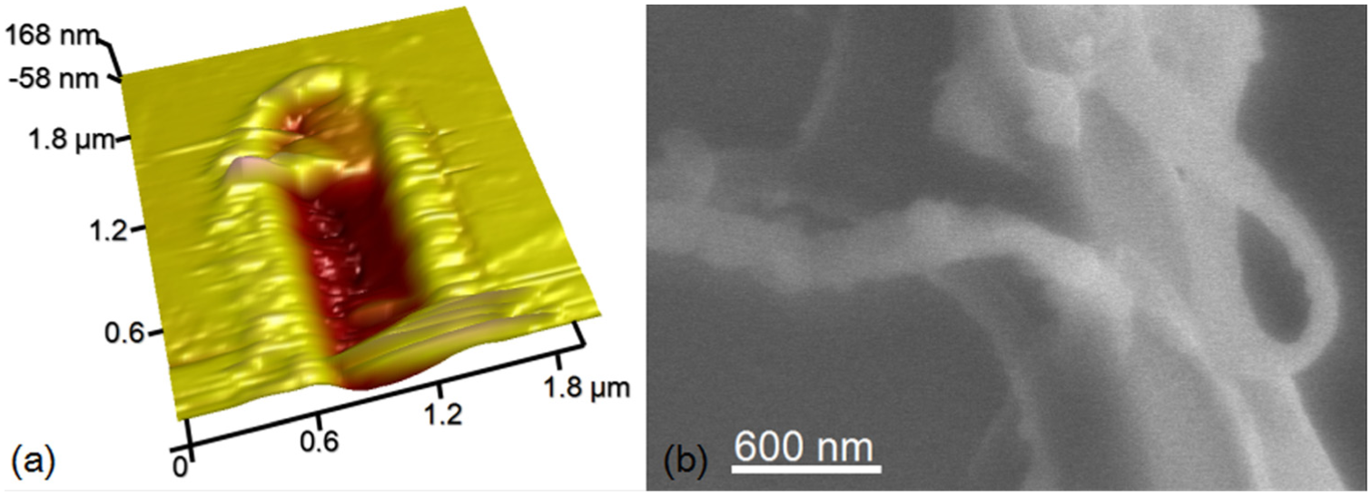
(a) AFM image of the nanochannel measured by contact mode. (b) SEM image of the AFM tip after the scratching process.
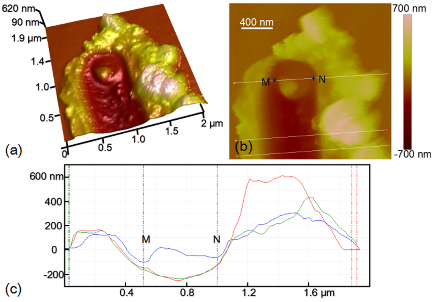
(a) 3D AFM image of the nanochannel measured by tapping mode. (b) 2D AFM image of the nanochannel and the corresponding cross-sections (c).
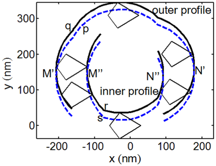
In Figure 5(a), it can also be observed that a circular protrusion is formed at the end of the machined groove. Figure 5(b) and (c) shows the 2D AFM image and the corresponding cross-section at three different locations on the groove. In particular, a cross-section is drawn in the middle of the formed circular protrusion mentioned above, denoted as line MN. Points “M” and “N” represent the two edges points of the bottom of the groove, respectively. In order to facilitate the analysis, the cutting trajectory above line MN is represented as Cycle 1, and the cutting trajectory below line MN is denoted as Cycle 2 in this study. Figure 6 shows the schematic of the cutting trajectory of the nanomilling process. In this particular scratching process, the amplitude of the rotary motion is around 470 nm, and the feed per circular motion is calculated as 10 nm. If these machining parameters are employed to make the schematic of the nanomilling process, the uncut chip thickness is too small to be observed in the schematic. Thus, to make the nanomilling process clearer, a relatively small amplitude of the rotary motion (300 nm) and a relatively large feed per circular motion (20 nm) are selected to draw the schematic of the nanomilling process in Figure 6. The direction of the feed is chosen to be along the y axis, and the cross-section of the tip at a height of 100 nm is employed. Although the machining parameters in Figure 6 show a small difference with the practical machining process, the conclusions obtained from this schematic should be similar. In Figure 6, the black solid line, named as “q,” represents the current cutting trajectory for Cycle 1, and the dotted blue line, denoted as “p,” illuminates the previous cutting trajectory for Cycle 1. Points M′ and N′ represent the intersection points of “q” and “p.” In addition, the black solid line, named as “r” in Figure 6, shows the current cutting path for Cycle 2, and the dotted blue line, indicated as “s,” illustrates the previous cutting trajectory for Cycle 2. Points M″ and N″ represent the intersection points of “s” and “r.” From Figure 6, it can be seen that the cutting angles and the edges of the tip participating in the scratching process change with different machining positions at the same probe height. Comparing the cross-sections at line MN and the completed machined locations of the grooves shown in Figure 5(c), the depth at line MN is much smaller. This indicates that both Cycle 1 and Cycle 2 contribute to the material removal to generate the nanochannel. From Figure 6, it can be found that the OA and OC edges of the probe are involved in the scratching process at the beginning of Cycle 1. The OA edge of the tip participates in the formation of the outer profile of the groove (scratching after M′ in Figure 6), and the OC edge takes part in the generation of the inner profile of the groove (scratching after N″ in Figure 6). Similarly, both OA and OC edges of the tip are involved in the scratching process for a period of time before the end of Cycle 2. The OA edge of the tip participates in the formation of the inner profile of the groove (scratching before N′ in Figure 6), and the OC edge takes part in the generation of the outer profile of the groove (scratching before M″ in Figure 6).
The machining trajectory of the tip in one scratching cycle corresponding to the cross-section of the tip with the height of 100 nm.
It can be found from Figure 5(a) that the removed material is mainly accumulated on the right side of the groove, while a smaller amount is also accumulated on the left side of the inner profile of the groove. The possible reason can be explained as follows. As shown in Figure 6, for the formation of the outer profile in Cycle 1 scratching process, the edges OC, OB, and OA of the tip participate in the machining process, and the feed values become larger and then decrease. Thus, the material is extruded by the AFM tip from right (point M′) to left (point N′), and the accumulation of the material is mainly formed at the second half scratching process of Cycle 1. When the tip reaches to point N′, the feed reduces to almost zero, and the direction of the scratching velocity is almost parallel to the right side of the nanochannel. This leads to most of the removed material accumulating on the right side of the groove in Cycle 1. Similarly, the feed values become larger and then decrease from right (point N″) to left (point M″) in Cycle 2, and the edges OC, OB, and OA of the tip also participate in the machining process. The material is pushed from right to left and piled up on the left side of the inner profile of the groove. Due to less material being removed in Cycle 2, the pile-up on the left side of the inner profile is much smaller than accumulations formed on the outer profile of the nanochannel.
Further discussions for the nanomilling process are conducted based on the analysis of the cutting trajectories of each edge of the tip in Cycle 1 and Cycle 2, as shown in Figure 7(a) and (b), respectively. The black dotted lines in these figures represent the trajectories of the projection of the probe apex in the horizontal plane. The red dotted lines, denoted “a,”“b,” and “c,” illuminate the trajectories of the edges OA, OB, and OC of the tip during the scratching process, respectively. To keep consistency with Figure 6, the black solid lines, named “q” and “r,” show the current cutting trajectories of Cycle 1 and Cycle 2, respectively, and the blue dotted lines, denoted “p” and “s,” represent the previous cutting trajectories of Cycle 1 and Cycle 2, respectively. In Figure 7(a), point I is the intersection of line “b” and line “c,” point K is the intersection of line “s” and line “c,” point J is the intersection of line “b” and line “a,” and point L is the intersection of line “s” and line “b.” In Figure 7(b), point H is the intersection of line “a” and line “b,” point G is the intersection of line “p” and line “a,” point F is the intersection of line “b” and line “c,” and point E is the intersection of line “p” and line “b.”
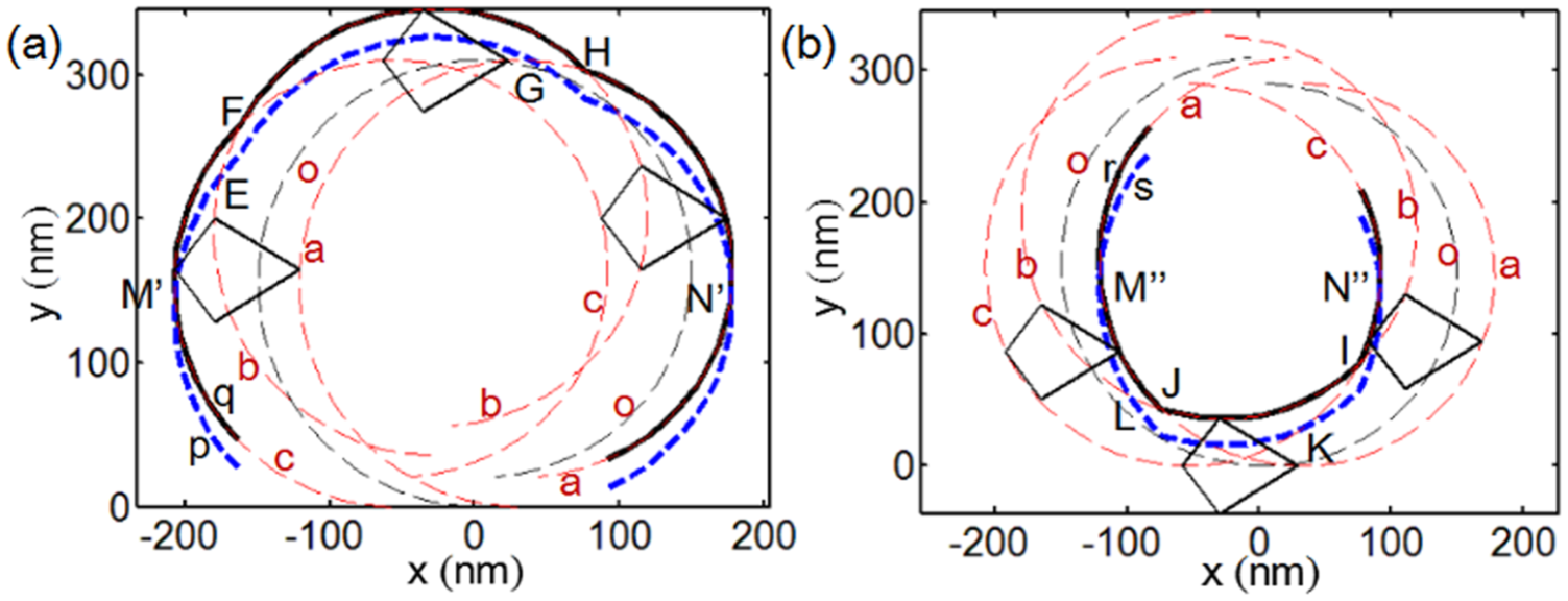
The machining trajectory of each edge of the tip in one scratching cycle corresponding to the cross-section of the tip with the height of 100 nm: (a) Cycle 1 and (b) Cycle 2.
As shown in Figure 7(a), only the edge OC participates the cutting process for the outer profile of the groove starting from point M′ at the beginning of Cycle 1. When the edge OB reaches point E, the edge OB starts to take part in the scratching process, and both the edges OC and OB are involved in the outer profile machining process at the same time. Once the edge OC reaches point F, it no longer participates in the scratching process in Cycle 1, and only the edge OB contributes to the machining of the outer profile of the groove. When the edge OA reaches point G, both the edges OA and OB participate in the scratching process. Similarly, once the edge OB reaches point H, it stops to take part in the scratching process in Cycle 1, and the edge OA cuts alone until it reaching point N′, which means Cycle 1 cutting process is finished. As shown in Figure 5, the machined depth for Cycle 1 is relatively stable. The possible reason for this phenomenon can be explained as follows. At the beginning of Cycle 1, the feed is relatively small, and the machined depth should be larger due to scratching with a constant normal load. However, the attack angle at this time is also relatively small, which may lead to enlarging the machined depth. For the period of the edge OB mainly taking part in the scratching process, the feed value rises comparing with the cutting process from point M′ to point F, which may result in a decrease of the machined depth. The attack angle becomes larger in this case, and this can cause an increase of machined depth. 24 After point H shown in Figure 7(a), only the edge of OA takes part in the cutting process. In this case, the feed value reduces and the attack angle is relatively larger, which can lead to the machined depth increasing. However, according to the discussion above, there is large amount materials accumulated in front of the tip at the end of Cycle 1, which can enlarge the contact area between the tip and the sample. This can result in a decrease of the machined depth. The cutting distances for the cases of two edges participating in the machining process (from point E to F and from point G to H) are relatively small, which can be neglected in the nanomilling process. Therefore, considering the effects of the feed value, attack angle, and the contact area between the tip and the sample, the stable machined depth for Cycle 1 is reasonable.
As shown in Figure 7(b), the edge OC of the tip participates in cutting from point N″ after Cycle 1. The edge OC moves from point N″ to point K to conduct the machining of the inner profile. The edge OB takes part in the scratching process from point I to point L, and the edge OA carries out cutting process from point J to point M″. It can be observed from Figure 5(a) that the machined depth exhibits an increase at the beginning of Cycle 2. According to the previous discussion, the edge OC participates in the inner profile machining, and the edge OA also conducts the cutting process of the outer profile at the beginning of Cycle 2. Due to the contact area between the tip and the sample for the edge OA, the influence of the edge OA can be neglected. Although the feed is increased at the beginning of Cycle 2, the increase of the attack angle may play a main role in the machining process leading to an increase of the machined depth. When the edge of OB is taking part in the machining process, the feed and the attack angle show almost no change, which can lead to a stable machined depth for the inner profile machining in Cycle 2, as illustrated in Figure 5(c). When the cutting edge OA starts to participate in the inner profile cutting process, a decrease of the machined depth with a distance before the end of the Cycle 2 can be found in Figure 5. The large pile-up of the material in front of the tip can also enlarge the contact area of the tip and the sample. This can lead to the decrease of the machined depth.
Conclusion
In summary, an AFM tip-based nanomilling machining method is utilized to fabricate nanochannels on a polymer PMMA surface in this study. The material is mainly removed in the forms of chips, which can be subsequently cleaned by the scanning process of the AFM tip in contact mode. The cutting angle of the main cutting edge of the tip during the nanomilling process is changing with the rotary motion of the sample, which may lead to a relatively large rake angle to generate chips. Moreover, relatively large feed values at the middle of the half cycle of the scratching process may also contribute to the formation of the chips. Due to the generation of the chips, the height of the material pile-up can be reduced. Moreover, the material is mainly accumulated on one side of the groove, and some material is also accumulated on the left side of the inner profile of the groove. The changes of the cutting edge and the feed value during the rotary motion are the possible reasons for this phenomenon. Furthermore, the scratching trajectories to obtain the outer profile and inner profile are also studied. The first half cycle is used to form the outer profile and the second half cycle is utilized to generate the inner profile and conducted the second scratching process to increase the machined depth. Finally, the change of the machined depth in one scratching cycle is investigated based on the scratching trajectories. The effects of the feed value, attack angle, and the contact area between the tip and the sample may be the possible reasons for the variation of the machined depth.
Footnotes
Declaration of conflicting interests
The author(s) declared no potential conflicts of interest with respect to the research, authorship, and/or publication of this article.
Funding
The author(s) received the following financial support for the research, authorship, and/or publication of this article: The authors gratefully acknowledge the financial supports of the Foundation for Innovative Research Groups of the National Natural Science Foundation of China (51521003), the National Natural Science Foundation of China (21327002), Self-Planned Task (SKLRS201606B) of State Key Laboratory of Robotics and System (HIT), the Program for New Century Excellent Talents in University (NCET-11-0812), and the National Program for Support of Top-notch Young Professors.