
Abstract
The method of a tip-based microscratching is used to fabricate micro/nano structures on single crystal copper (110) and (111) planes under room temperature. The surface-enhanced Raman scattering enhancement performance of the structured Cu surface has been studied by rhodamine 6G probe molecules. Such micro/nano structures can be machined by varying the scratching parameters such as the feed and the normal load. Experimental results show that the high surface-enhanced Raman scattering enhancement is attributed to the nanostructures formed by pile-ups between adjacent grooves and nanocracks at the bottom of the microsquare. In addition, the Raman intensity of the crystallographic plane (110) is stronger than that of the crystallographic plane (111). This work verifies that the microscratching method is a feasible way to machine active surface-enhanced Raman scattering substrates on Cu surfaces with low cost and high efficiency.
Introduction
Nowadays, active substrates of surface-enhanced Raman scattering (SERS) have attracted considerable attentions due to the ability of detecting molecules and inspecting the interaction between molecules and metal surfaces.1–3 Some chemical methods,4–6 including chemical/electrochemical deposition, 4 electrochemical etching, 5 and hydrothermal process 6 are often employed to fabricate SERS substrates. However, the uniform distribution of materials at different positions on the generated SERS-active substrate is difficult to be controlled and localized, and the “hot spots” for SERS enhancements cannot be easily reproduced. In addition, the chemical method to fabricate SERS substrates has a potential shortcoming of contaminating the environment. Some other researchers utilized the nanosphere lithography 7 and focused ion beam (FIB) 8 methods to produce micro/nano structures as the SERS substrates. The lithography principle–based method, however, is still more expensive than other methods. The resolution of nanostructures fabricated by FIB is significantly high. But the cost of the FIB method is also very high, and it owns the property of low throughput. 9 Therefore, the micro/nano mechanical machining method is employed by some scholars, which owns the high machining efficiency and is controllable to fabricate complex two- and three-dimensional micro/nano structures.10–13 For example, the polymethyl methacrylate was machined with nanometric surface roughness by the micro-milling method. 10 This approach can machine complex microstructures on many workpiece materials. 11 The diamond tool flycutting is a good method to achieve the ultra-smooth surface which can also be used to machine microstructures. 12 Additionally, the commercial nanoindenters were already used to fabricate SERS substrates by the nanoindentation tests. 13 However, the nanoindenter is still primarily a measurement device. The shortcomings of high cost and low machining speed of this method are the main barriers to achieve industrial applications as a micromachining device. Therefore, in this work, based on a home-built system, we use the microscratching method to fabricate the substrate with micro/nano structures on Cu (110) and (111) planes with high efficiency and low cost. The substrates formed by this method have been verified to be high repeatability and can be used as the active SERS substrate.
Experimental details
A low-cost home-built micromachining system is developed for fabrication of micro/nano structures in our previous works. 14 The pyramidal diamond tip is employed as the scratching tool presented in Figure 1. The tip radius is <200 nm. As shown in Figure 1(c), the tip’s motion is realized by the nano accuracy stage. d and f represent the width of the microsquare and the machining feed, respectively. The feeding and scratching directions are along the Y and X directions. The normal load F of <500 mN is employed. More details about this system can be found in Yan et al. 14 It only takes several seconds to machine single microsquare.
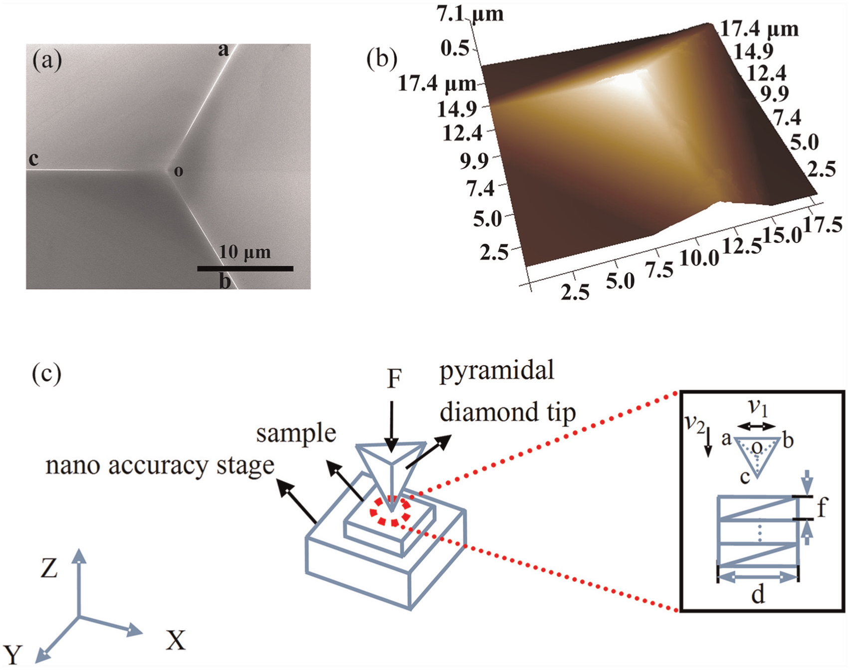
(a) SEM and (b) AFM images of the cube corner tip and (c) schematic diagram of machining microsquare.
The samples are single crystal copper (Cu (100) and Cu (111)) of 10 mm × 10 mm × 1 mm. The roughness (Ra) is <5 nm. The atomic force microscope (AFM) system used to image the machined structures is Dimension Icon (Bruker, Germany). After machining, the copper samples are dipped into water solution of rhodamine 6G (R6G) for 30 min and dried with a continuous gentle nitrogen blow. Raman measurements are examined by a Renishaw inVia Raman system using the 633-nm HeNe laser. The incident optical power is 6.4 mW. The beam diameter is about 1 µm.
Results and discussion
Fabrication of microsquares and SERS measurements on Cu (110) plane
Figure 2 shows typical AFM images of microsquares on the Cu (110) plane with a normal force of 5 mN and a machining velocity v1 of 100 µm/s. The feeds of 2500, 2000, 1600, 1200, 1000, and 800 nm are employed. As shown in Figure 2(a)–(c), from the morphologies of the upper and down sides of the machined squares, it can be found that the surface pile-up is a major style of material removal when scratching the Cu (110) plane, and more pile-ups are generated with a decrease in the feed. Additionally, as shown in Figure 2(d) which is an enlarged picture of the local position of Figure 2(c), nanocracks are formed at the bottom of the microsquare with the feed of 800 nm.
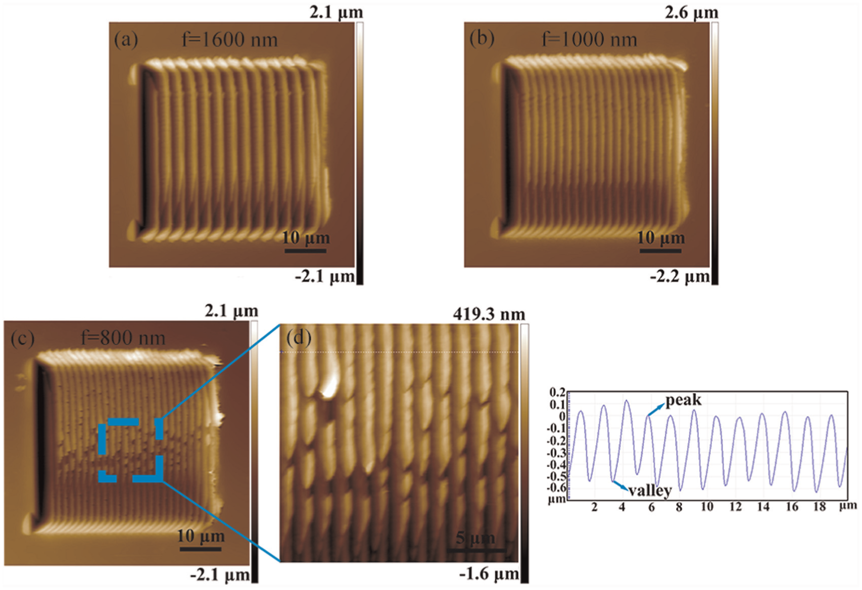
AFM images of microsquares on Cu (110) plane: (a) the feed of 1600 nm (b) the feed of 1000 nm (c) the feed of 800 nm and (d) an enlarged picture of the local position of Fig. (c).
Figure 3 shows Raman-active peaks of R6G molecules on the microsquares. The concentration of the R6G solution was 10−5 M. A clear enhancement is observed in the Raman signal from R6G on the machined structures (normal force is 5 mN), as shown in Figure 3(a). Characteristic peaks of R6G molecules are shown at 771, 1183, 1311, 1360, 1504, and 1603 cm−1, respectively. It can be observed that the SERS effects of the Raman intensity are remarkably affected by the feed f.
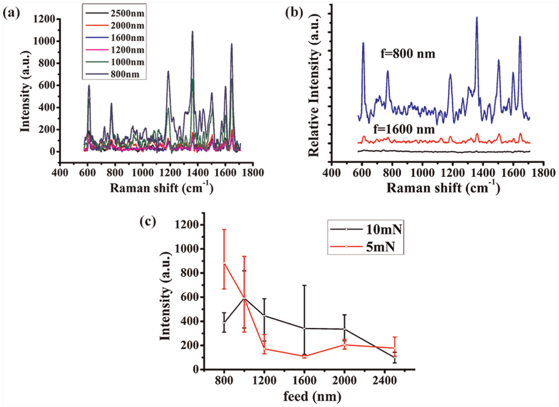
Raman-active peaks of R6G molecules on Cu (110) substrate at a concentration of 10−5 M: (a) Raman intensities of R6G molecules with different feeds (b) relative Raman intensities for bare substrate, the microsquares machined by the feeds of 800 nm and 1600 nm (c) the average Raman intensity of the 1360 cm−1 R6G of 30 μm×μm area.
Figure 3(b) shows the relative Raman intensities for the bare substrate, the microsquares machined by the feeds of 800 and 1600 nm with the normal force of 5 mN. The Raman intensity is the smallest for R6G on the bare substrate. The Raman intensity for the feed of 800 nm is stronger than that for the feed of 1600 nm. This result is attributed to more nanocracks formed at the bottom of the microsquare with the feed of 800 nm, as shown in Figure 2(c) and (d). The observed signal enhancement induced by the nanostructures (called “nanocracks,” in this study) may be due to the enhanced near-field associated with this resonant mode and chemical enhancement. 2 R6G was presumably entrapped within the nanocracks in the microsquare and noticeably detected by the SERS effect.
Figure 3(c) shows the average Raman intensity of the 1360 cm−1 R6G of 30 µm × 30 µm area. The intensities do not change obviously with the feed range from 1200 to 2500 nm when the normal force is 5 mN. However, the intensities increase abruptly when the feed becomes small ranging from 800 to 1200 nm. Because nanocracks generated by a small feed improve the chemical adsorption for R6G molecules on the peak of the microsquare and perfect sinusoid type microstructures induced by the diamond tip’s shape in the microscratching process do not obviously improve the Raman intensity. When the normal force is 10 mN and the feed is 1000 nm, the peak intensity is stronger than that of other feeds.
Fabrication of microsquares and SERS measurements on Cu (111) plane
In this section, the same feed and normal force are employed. The Raman intensities were not detected by the 10−5 M R6G solution on the Cu (111) plane. Therefore, the concentration of 10−4 M R6G solution was used in this section. Figure 4(a) and (b) represents the AFM images of the microsquare with nanostructures rather than the nanocracks at the peak using the feed of 2000 nm and the normal force of 10 mN. From three sections, the vertical distances of these nanostructures are 127, 125, and 115 nm, respectively. Nanostructures disappear when the feed is 1600 nm, as shown in Figure 4(c) and (d).
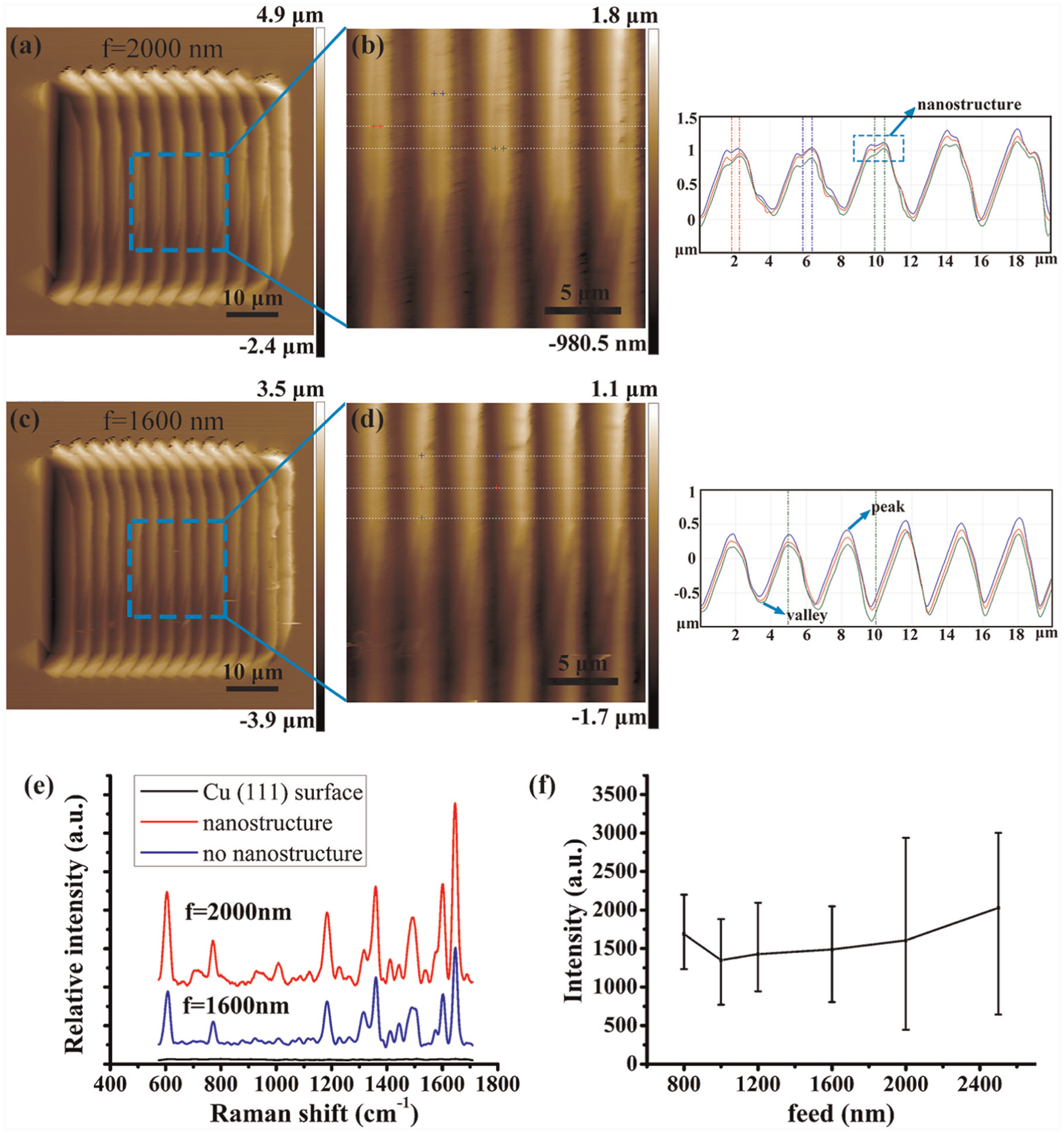
AFM images of microsquares on Cu (111) and Raman-active peaks of R6G molecules at a concentration of 10−4 M: (a) and (b) AFM images of the microsquare with the feed of 2000 nm (c) and (d) AFM images of the microsquare with the feed of 1600 nm (e) Raman intensities of R6G molecules for the bare surface, the feed of 1600 nm and the 2000 nm (f) the average Raman intensity of the 1360 cm−1 R6G of 30 μm × 30 μm area.
The Raman intensity for the feed of 1600 nm is lower than that for the feed of 2000 nm as shown in Figure 4(e). The Raman intensity is the smallest for R6G on the bare Cu (111). Figure 4(f) shows the average Raman intensity of the 1360 cm−1 R6G of 30 µm × 30 µm area. The average intensity of the feed of 2500 nm is the strongest because nanostructures may adsorb more probe molecules. When the feed changes from 800 to 2000 nm, the intensity does not obviously change. When the feed varies from 2000 to 2500 nm, the intensity at the peak increases only and change a little at the valley. R6G was presumably entrapped within such nanostructures in the microsquare.
The enhancement factors are calculated as follows15,16
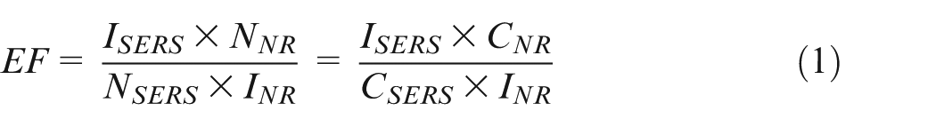
where ISERS and INR are the intensity of SERS and normal Raman scattering intensity, respectively; NSERS and NNR are the number of molecules evaluated by SERS and normal Raman scattering measurements, respectively; and CSERS and CNR are the concentrations of SERS and normal Raman measurement, respectively, with a 0.02 M R6G solution on a SiO2 wafer. The SERS enhancement factors of micro/nano structures machined by a tip-based microscratching in this study are 2.75 × 10⁵ for single crystal copper (100) plane and 5 × 10⁴ for single crystal copper (111) plane.
The Raman intensity of single crystal copper (110) plane is greater than that of the single crystal copper (111) plane. This result is similar to other researchers’ conclusions.17,18 Surface energies γ of different crystallographic planes are usually different for the face-centered cubic structured metal, and a general sequence may hold, γ(110) > γ(100)> γ(111). Therefore, the higher the surface energy of the crystallographic plane, the stronger its reaction with the adsorbed probe molecules. Finally, the Raman intensity of the crystallographic plane (110) is the strongest among other crystallographic planes.
Conclusion
In summary, using a tip-based microscratching machining method, complex nanostructures by surface pile-ups induced by adjacent grooves and nanocracks formed by the tip’s trace are obtained on the copper substrates. These micro/nano structures can be controlled by the tip’s feed and the crystal plane. The SERS intensity induced by such kinds of nanostructures for the R6G molecules is verified through experiments. The SERS enhancement factor is 2.75 × 10⁵ for Cu surface, which is comparable to the previous studies’ conclusion. The tip-based microscratching, a simple, repeatable, and highly efficient method, has a great potential to machine the SERS substrates.
Footnotes
Declaration of conflicting interests
The author(s) declared no potential conflicts of interest with respect to the research, authorship, and/or publication of this article.
Funding
The author(s) disclosed receipt of the following financial support for the research, authorship, and/or publication of this article: This work was financially supported by the Foundation for Innovative Research Groups of the National Natural Science Foundation of China (51521003), the National Natural Science Foundation of China (51675134), Self-Planned Task (SKLRS201606B) of State Key Laboratory of Robotics and System (HIT) and the National Program for Support of Top-notch Young Professors.