
Abstract
This article provides the design and fabrication details of a new technique to build a microfluidic device with two parallel substrates and a silicone gasket. The fabrication process uses screen printing technology offering fast and low-cost microdevices without the need for high-cost fabrication equipment and special photoresist processes. Hermetic microfluidic channels of 300 µm width and 50 µm height having parallel facing electrodes on two substrates are made with simple serigraphy technique using silicone rubber. The fabricated devices were experimentally tested for detection and characterization of polystyrene particles and living cells by negative and positive dielectrophoresis. The reported technique enables simple manipulation, centering, detection and characterization of living cells at low and high frequencies.
Keywords
Introduction
The emergence of new technologies such as micro-electro-mechanical systems (MEMS) associated with microfluidics and Lab-on-a-chip concept brings new type of available tools with the possibility to perform efficient and low associated tests and assays with very little help of the human operator. The introduction of Bio-MEMS technology1–3 created a synergy between medical and engineering researchers. The ultimate objective is to reproduce the same laboratory biological assays with miniaturized Bio-MEMS devices with acceptable specific and sensitive results. Initial investigations have proved that Bio-MEMS will be able to enrich the preventive capability of the laboratory assays through functions that yield more accurate diagnostics, earlier captive or better prognostics of medical conditions.
Diversity of microfluidic chips or devices has been used by researchers for different applications with different designs and fabrication processes and methods using structures made by plastics such as polymethylmethacrylate (PMMA),4–8 glass and silicon. Channels and microdevices are constructed with SU-8 epoxy based negative photoresist and polyimide.9–19 Other channels are embedded in polydimethylsiloxane (PDMS) presenting unique features and allowing 2D electrode systems for protein and cell manipulations.10,20–26 For substrate material of PMMA, silicon and glass substrate, processes such as dry etching, wet etching, injection molding, laser ablation and high temperature stamping/embossing or imprinting are used to create channels. Hermetic sealing is achieved using wafer level bonding and adhesive film bonding requiring high temperatures.9,11,17,22
Dielectrophoretic (DEP) manipulation and centering of particles involve the principle of applying an AC harmonic signal, with proper frequency and amplitude, on two electrodes of different geometries creating a non-uniform electric field. DEP refers to the movement of electrically neutral but polarizable particles in a non-uniform electric field. When the particle moves toward the gradient of electric field maxima and gradient of electric field minima, then the DEP phenomenon is specifically termed as positive-DEP (pDEP) and negative-DEP (nDEP), respectively. The AC signal with the designed electrodes creates non-uniform electric field and uncharged particles move under polarization effect.27–30 Knowledge of the crossover frequency of each type of cell in the suspended media determines the transition from nDEP to pDEP. Crossover frequency is dependent on low-frequency dielectric properties of the living cells and the media.30,31
This research article presents the complete design and fabrication procedure of a fast and low-cost microfluidic device obtained by screen printing or serigraphy of patterned silicone rubber layer on fused silica having gold patterned parallel facing electrodes with different geometries. Validation of the operation of the microfluidic device is confirmed by cells manipulation using DEP. nDEP and pDEP are verified on polystyrene microspheres and Saccharomyces cerevisiae or budding yeast cells.
Methods
A microfluidic device is fabricated to enable observation, manipulation, detection/counting and characterization of biological cells suspended in media. The microdevice includes several patterns of electrodes deposited on both substrates—top and bottom. In order to observe cells or particles moving in the channel with a microscope, two practical solutions are available for substrate material, namely, transparent plastic or glass. PMMA material showed some difficulties of warping while depositing electrode materials by sputtering technique due to the high temperatures occurring during deposition process. Use of cyclic olefin copolymer (COC) supporting high temperatures would be a solution, but it has some disadvantages in precision of photolithographic process and achieving low electrical resistivity electrodes with simple deposition process. 32 It was not possible to use PDMS to make the channel because of the presence of parallel facing electrode configuration on both sides of the microfluidic device, top and bottom. Since the height of the channel is set to be in the range of 50–80 µm to enable high DEP force in the microdevice and to avoid any clogging of cells, several solutions are considered to create microfluidic chip. Double-sided adhesive tape with certain thickness (ARclearTM 8154; Adhesives Research, USA) and patterned with desired shape of channel could be used to create 3D channel. This solution could ensure a hermetic microfluidic chip but microscopic alignment of the parallel facing electrodes for a specific design would become a difficult task due to tight dimension specifications at electrode overlapping stage and complex alignment manipulation of double-sided adhesive, requiring specialized sophisticated alignment equipment. Photo-imageable film could be used to form the channel by photolithography. This material is commonly used in photolithography of printed circuit board (PCB), but the issue of hermetic channel sealing is difficult to overcome at the edges of the substrate when glue is used. It is noted that any liquid glue can infiltrate by surface tension, diffusion or dispersion and can clot the channel. Moreover, use of alcohol and other solvent for subsequent sterilization stages limits the use of this film given its solubility with alcohol or other solvent. SU-8 or polyimide made channel would be a good solution. Nevertheless, this solution is not considered to circumvent the use of SU-8 or polyimide high-cost process and high temperature and pressure hermetic sealing equipment. In fact, SU-8 process environment is not a standard available process in many laboratories, and high-cost equipment with a pressure of about 1.9 MPa and a temperature of about 175 °C is needed to ensure an acceptable bonding for hermeticity. 33 Therefore, the solution provided in this work resides in creating microchannels with screen printing silicone rubber (GE112A, General Electric) on the fused silica wafer with a metal mask made at the desired shape and height of the channel. Silicone rubber screen printing technique is the core topic and challenge of this research. Silicone rubber is biocompatible, resistant to solvents and cleaning solutions used in clinical applications. The most important characteristic is its softness after curing, permitting a perfect sealing of the channel. To ensure the hermetic sealing of the device, two aluminum plates retain the two substrates as shown in Figure 1. The tightening of the two aluminum blocks with four screws ensured the hermetic sealing of the microfluidic chip.
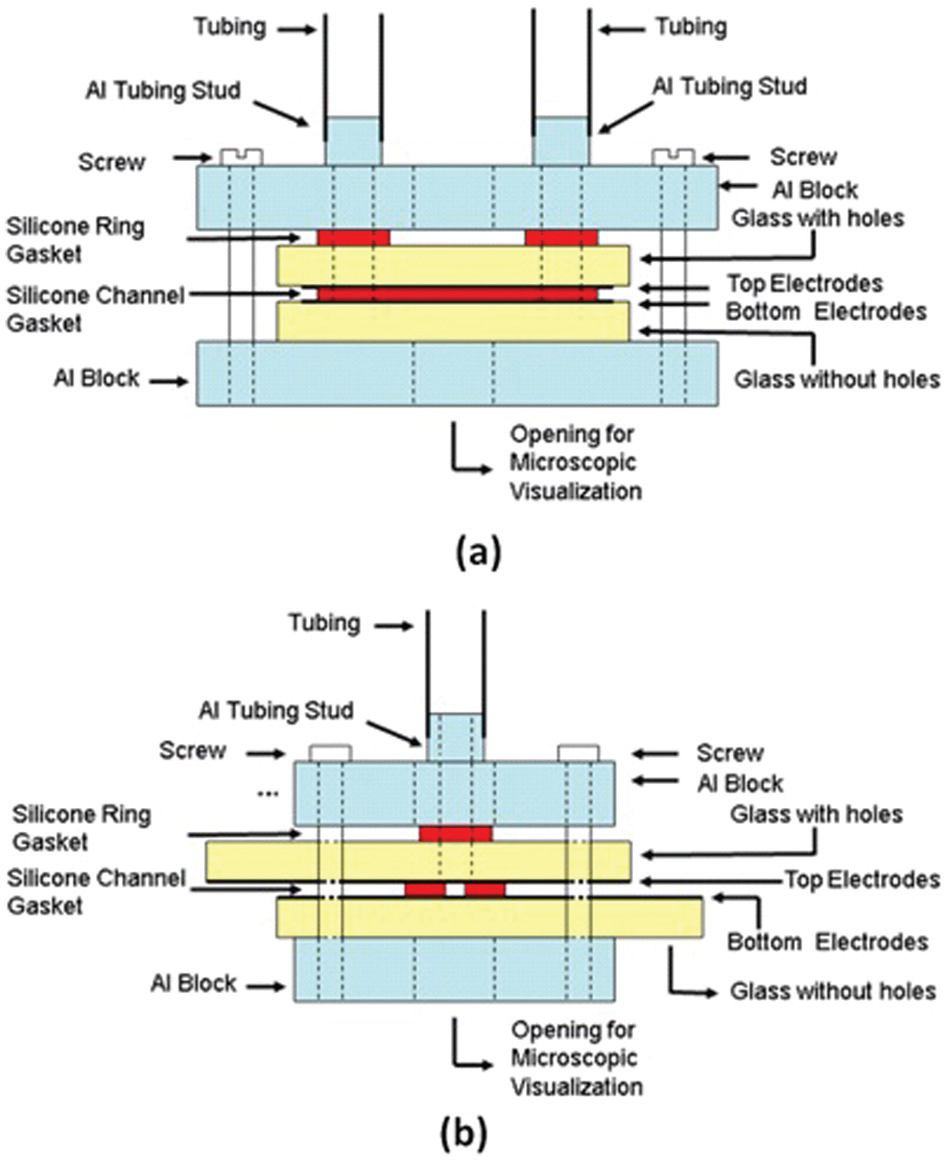
(a) Cross section view of the entire fabricated microdevice. (b) Side cut view of the entire microdevice.
Glass material was initially used as substrate but it showed some fabrication problems. Glass substrates crack when aluminum plates are pressing the two substrates. Moreover, inlet and outlet openings, made by laser ablation or by alumina powder abrasion, showed some micro cracks in glass, creating serious issues related to leaks in the microdevice. These problems are not observed when fused silica glass is used as substrate material. This is due to its good mechanical, thermal and electric properties compared to PMMA and glass. Inlet/outlet openings in the microfluidic device were created by alumina powder abrasion. The reported fabrication process of microfluidic systems is simple, fast and low cost, and provides a 3D hermetic channel having integrated facing electrodes on the two sides of the device, top and bottom. Manual alignment precision of the two substrates is better than 10 µm. The alignment of the facing electrodes overlapping was performed under a microscope. Trapezoid and Y-shaped Au electrodes are deposited using a sputter machine (Q300TT Sputter Coater) and standard photolithography etching process. Electrodes are made on the top and bottom substrates, creating parallel facing electrodes. These trapezoidal electrodes are intended for cell focusing at the center of the channel by nDEP. Other electrodes are present to detect, count and characterize cells at low/high frequencies. Inlet and outlet ports are made of aluminum insert studs within the aluminum block, giving more mechanical resistance to applied pressure from inlet/outlet tubing. These ports are connected to the glass structure via the holes in the studs. Sealing between fused silica holes and the aluminum block studs is ensured with the silicone rubber rings. Figure 1(a) and (b) shows cross section and side cut view of the entire microfluidic channel structure. Top and bottom electrodes identified on Figure 1 represent the parallel facing electrodes needed for the manipulation and detection of cells. In summary, fused silica glass is the final choice for the substrate material given its mechanical and optical properties. On these substrates, thin gold film is deposited for its biocompatibility and low resistivity. The thin film fabrication process is based on wet etching using standard lithography. Prior to the lithographic procedure, a set of masks was prepared to pattern the desired electrodes structure.
The steps for printing the electrodes on the substrate are the following:
The metal is deposited by sputtering (Plasma Science Inc. Model 150). A layer of 20 nm Ti (as adhesion coating) is followed by a layer of 1 µm of Au.
The photoresist (AZ1518) is spun having a final thickness of 3 µm.
The mask is aligned to the substrate and exposed with standard ultraviolet (UV) mercury lamp integrated to the mask aligner (OAI, Model 200).
This photoresist (AZ1518) is developed to get the desired electrode pattern.
The Au is etched using iodine solution at room temperature for 2 min.
The Ti is etched using hydrogen peroxide 35% at 70 °C for 10 min.
The resist is stripped off and the substrate is cleaned with acetone.
The thin film process simplified block diagram is given in Appendix 1. Those steps were repeated for the second substrate using the same mask 1. The first substrate is at the bottom of the structure and the second substrate is at the top of the structure. On the second substrate, two holes are required to allow the fluid to pass through the microfluidic channel.
The fabrication steps are the following: cutting the substrates, patterning the electrodes, drilling the holes, creating the channel and the rings from silicone rubber, and finally assembling the device with aluminum blocks for hermetic sealing.
After cutting the substrates and patterning the electrodes on the substrate, two holes were drilled by alumina powder abrasion. Then, a thin layer of silicone rubber is applied using the screen printing technique. The pattern of silicone rubber to create the microchannel is printed on one layer of the substrate. Ring patterns of silicone rubber are made surrounding the holes on the second substrate. Then, the two substrates were aligned under microscope after silicone was cured at room temperature. In the final step, the two substrates are mounted between two aluminum blocks, and the entire unit is tightened by screws on each corner to ensure that no leaks on the channel and connection ports are present. The patterned brass screens for the microchannel and the sealing rings are shown in Figure 2(a) and (b).
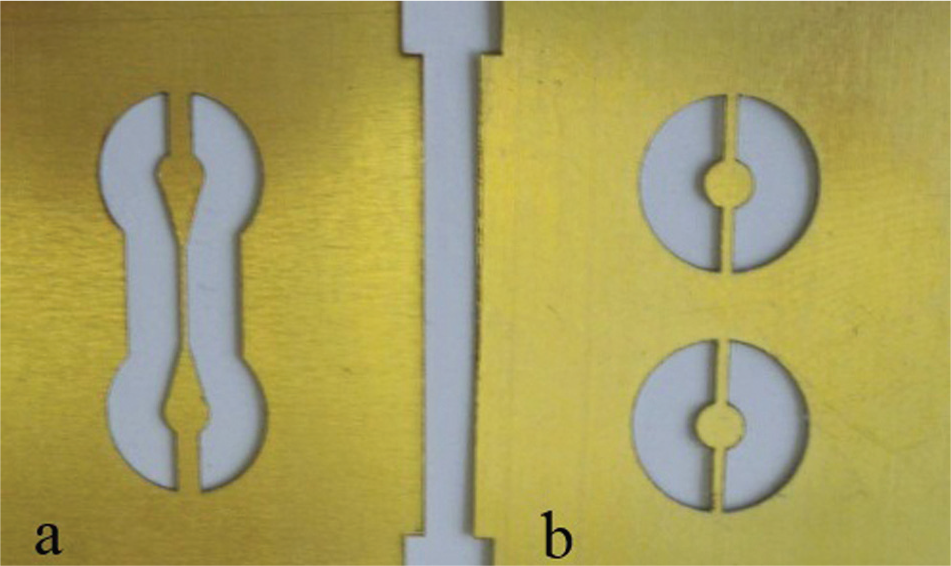
Patterned screens used for screen printing the silicone rubber. (a) Mask 1 for substrate 1 is used to create the microchannel and (b) mask 2 for substrate 2 is used as the sealing rings.
Figure 3(a) shows a picture of the created channel with silicone rubber on the substrate. The white colored material on the top of the fused silica substrate represents the silicone rubber that forms the microchannel. In Figure 3(b), a blow-up picture through the opening shows the Au electrodes inside the microchannel. Figure 4(a) shows a picture of assembled structure of microfluidic device. Figure 4(b) shows a picture of the microfluidic device associated with all the electronic circuits for the focusing of cells to the interrogation point, for the detection, the counting and the characterization of cells at low and high frequencies.
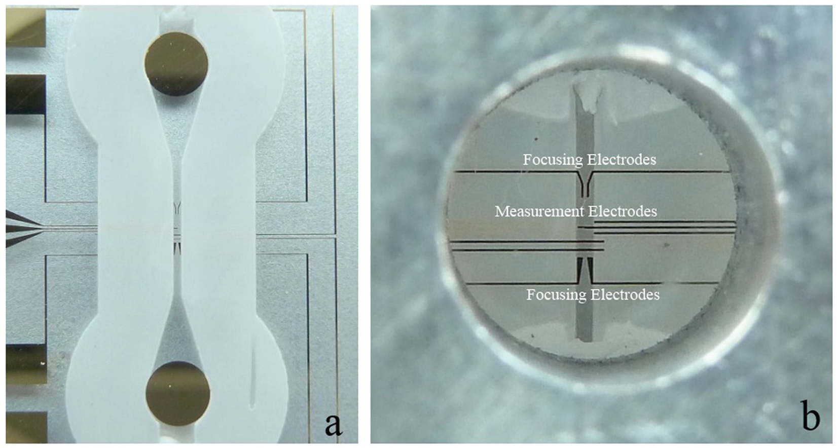
(a) Silicone rubber screen printed on fused glass with gold deposited electrodes. (b) Close up picture, through the aluminum blocks’ opening, of the microchannel with the focusing and measurement electrodes.
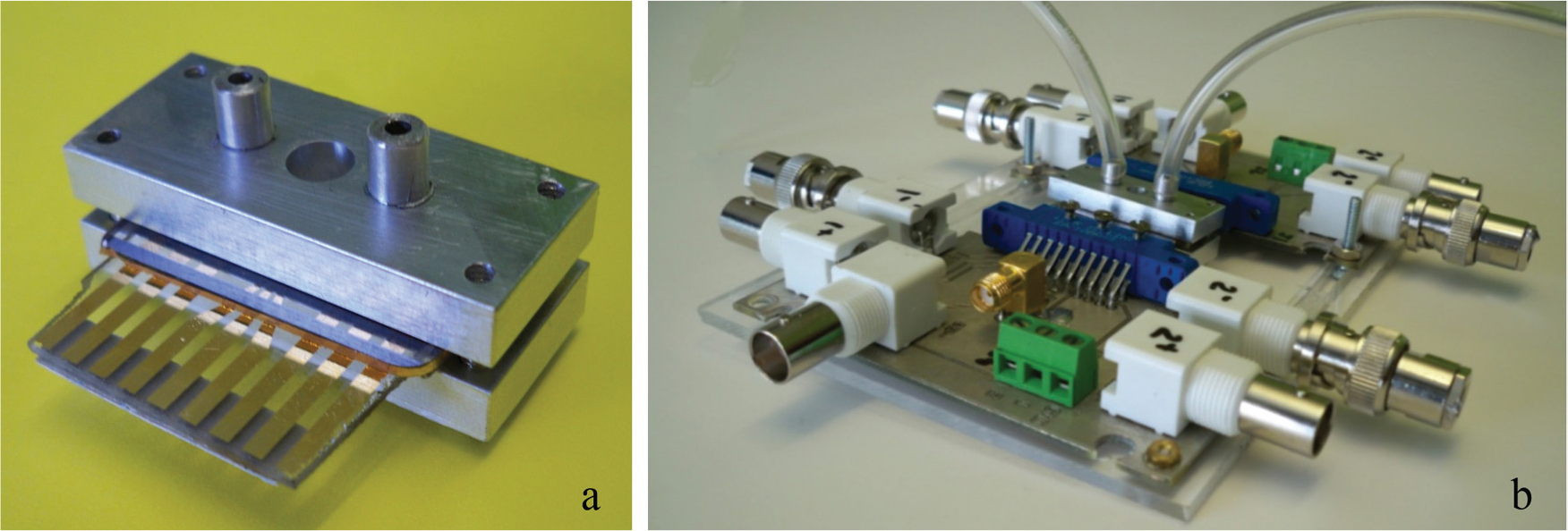
(a) Assembled structure of the microfluidic device. The two fused silica glass substrates are pressed together with two aluminum blocks. The patterned electrode material is in gold. The two studs on the top of one of the blocks are the inlet and outlet of the microfluidic device. The opening at the middle of the block is for the visualization of the microchannel under the microscope. (b) Integrated microfluidic channel with electronic circuits for system control and measurements. Connectors for DEP centering, low and high frequency measurements are incorporated in the circuit.
Results
The fabricated microdevice was experimentally tested to manipulate cells and particles. Multiple operation of the microfluidic device is demonstrated on polystyrene beads and Saccharomyces cerevisiae cells. DEP experimentation is performed using non-uniform electric field created by focusing patterned electrodes. Parallel facing electrodes in the microchannels are designed to create non-uniform electric field enabling DEP sorting of cells/particles. These electrodes are connected to AC voltage through electric wires. Figure 5 shows the electric connection of the electrodes to the low-frequency generator to create nDEP and pDEP forces. Attraction and repulsion of cells were observed under the microscope by varying the applied AC signal frequency. AC generator (RIGOL DG4062) was set to amplitude of 10 V peak to peak with variable frequencies from few KHz to 20 MHz. Different shapes of trapezoidal electrodes giving non-uniform electric field and inducing positive gradient of the electric field are designed to focus cells at the center of the microchannel 34 followed with other patterned electrodes for cell or particle detection and characterization at low and high frequencies. Control parameters used for nDEP and pDEP effects are media conductivity and the applied signal frequency on focusing electrodes.
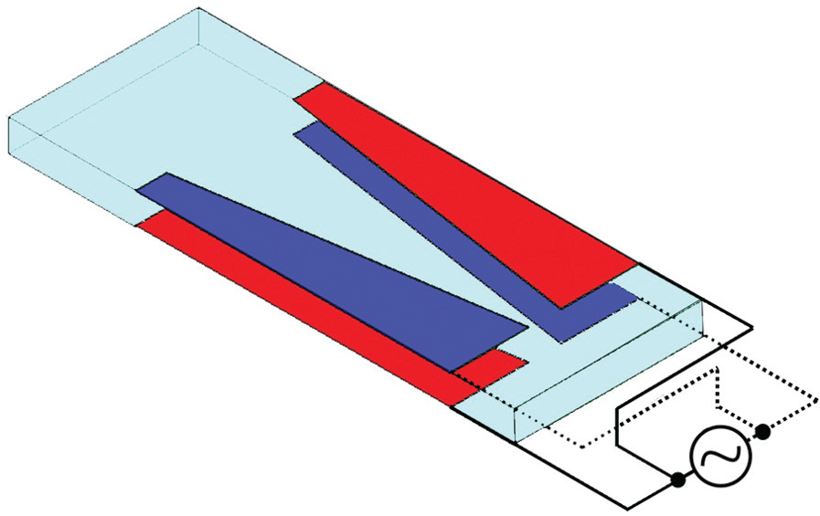
Electric connection of trapezoid electrodes to the AC generator. Depending on the dielectric property of the particle and the applied frequency, particles are subject to nDEP or pDEP.
Channel operation is verified and good operation is validated by investigating the nDEP and pDEP effect on microparticles and living cells. These particles and cells are diluted or suspended in prepared media. Suspended particles or cells are injected through the inlet port of microfluidic device through a syringe pump. The syringe pump “Pump 11 plus” from Harvard Apparatus, Inc. has characteristics of volume flow rates of 0.0014 µL/h to 474.6 mL/h. A syringe of 1cc volume is used with low flow rates of about 6 µL/h. Channel hermeticity was verified by injecting distilled water with different flow rates. Microfluidic chip preserved its integrity and no liquid leak was observed within the channel after multiple experimentations.
Figure 6 shows the movement of the 15 µm polystyrene bead within the channel with the beads focused at the center of the trapezoid electrodes of the channel by nDEP. The conductivity of the media was set to 20 mS/m. The applied voltages on trapezoidal electrodes are 10 and 0 V on opposite electrodes and the frequency is set to 500 KHz. In Figure 6, several snap pictures (a, b, c and d) show the movement of the 15 µm diameter beads through the focusing electrodes (flow direction is from bottom to top). Particles were successfully centered in the microchannel using the fabricated microdevice.
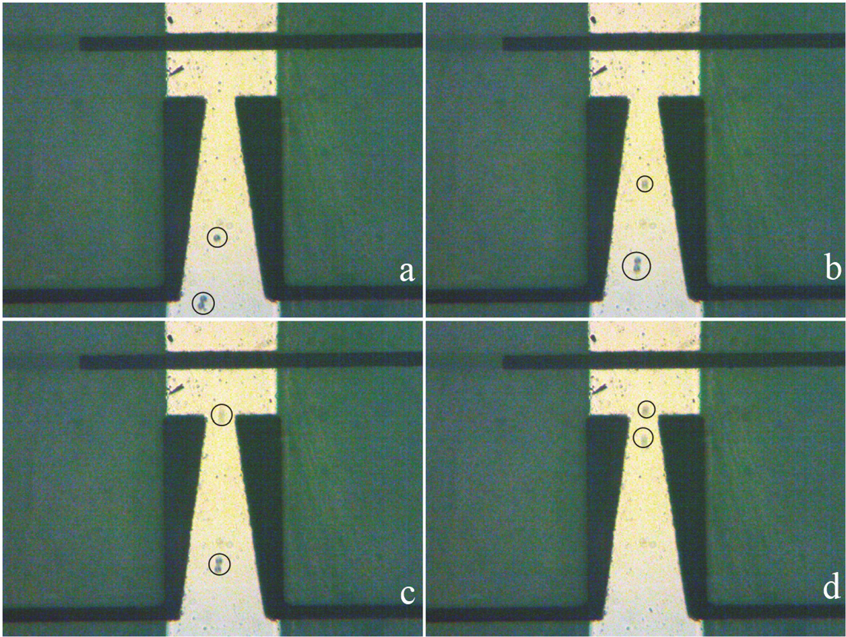
Polystyrene beads movement (pictures a–d) within the center of the microchannel. The polystyrene bead diameter is 15 µm and the flow rate is 6 µL/h. The conductivity of the media is 20 mS/m. The AC signal frequency is 500 KHz with amplitude of 10 V peak to peak.
Figure 7(a) and (b) shows the movement of the bulk Saccharomyces cerevisiae yeast cells within the microchannel fabricated using the method presented. The media conductivity was 330 mS/m; the signal frequency was 500 KHz with amplitude of 10 V peak to peak. Under these conditions, nDEP effect was observed on the yeast cells. Clearly, the cells (identified by arrows) were repulsed from the edges of the trapezoidal and Y electrodes and are focused to the center of the channel. Figure 7(c) and (d) show the effect of pDEP on the yeast cells under the same conditions except with a frequency of 2 MHz. In this case, the cells are attracted and gathered at the edges of the trapezoid and Y electrodes.
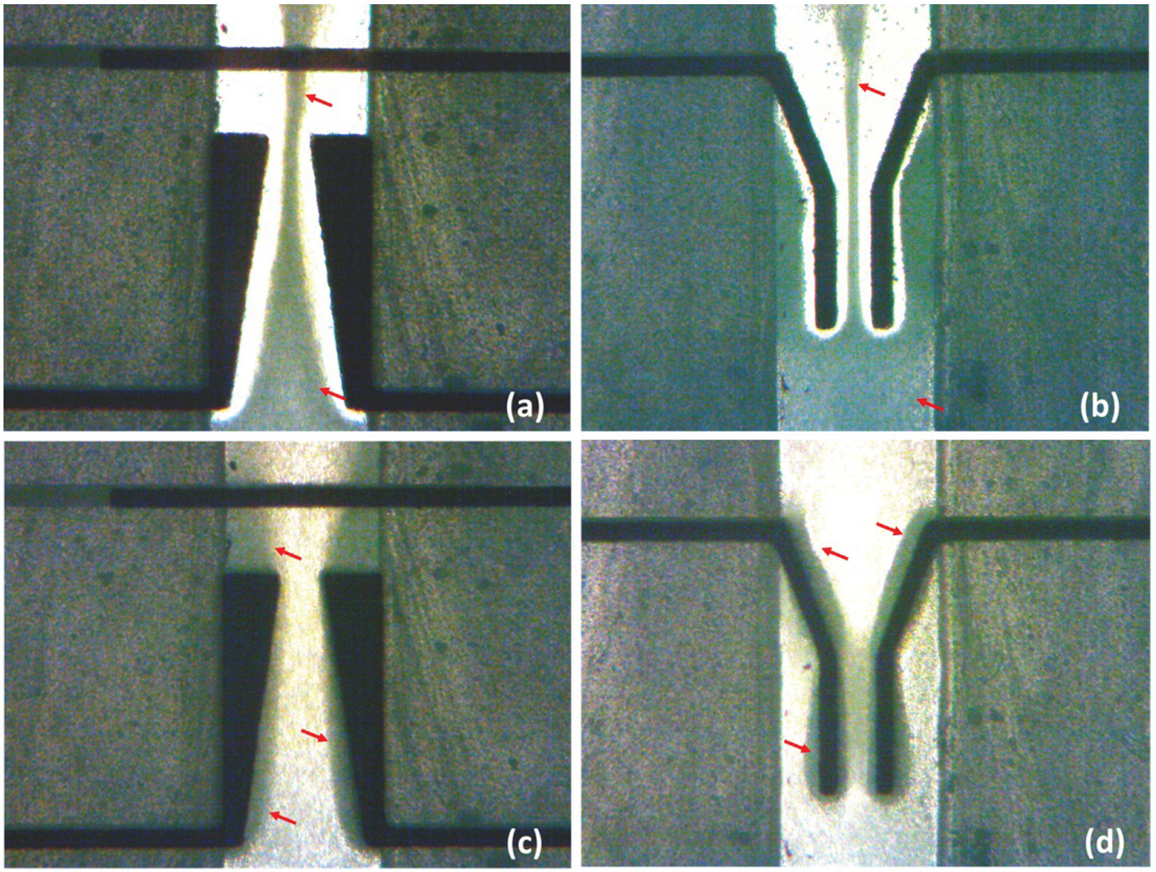
(a and b) Bulk stream of yeast cells movement under nDEP within the center of the microchannel between trapezoid and Y electrodes and (c and d) their movement under pDEP. The flow rate is 6 µL/h. The conductivity of the media is 330 mS/m. The AC signal frequency is 500 KHz for nDEP and 2 MHz for pDEP with amplitude of 10 V peak to peak.
Discussion
Fused silica and silicone rubber are used for the substrate and microchannel material respectively to create the microfluidic channel. Serigraphy technique with silicone rubber is used as low-cost and simple method of prototyping of microfluidic devices. The alignment of the two substrates for facing electrodes on two substrates was achieved within few minutes under a microscope with the help of alignment marks. A special jig could be made for alignment of a large number of devices. The two fused silica substrates are sandwiched between two thick blocks of aluminum plates. Four screws at the edges of the blocks tightened at the proper torque ensure the sealing of the channel. Several patterns of electrodes were added in the microfluidic device to manipulate particles and living cells. The operation and hermeticity of the microfluidic channel are validated by verifying the DEP operation in the microchannel and with several hundred operations with the same device. Several units are assembled with parallel facing electrodes. For all these units, the alignment of parallel facing electrodes is always less than 5 µm. DEP operations are repeated and 3D focusing of particles within the microchannel is ensured for all particles without exception.
In conclusion, a simple, low-cost and fast microfluidic device with 300 µm width by 50 µm height channel is fabricated using two fused silica substrates and screen printing silicone rubber acting as a gasket. A hermetic microfluidic chip is fabricated with parallel facing electrodes for cells/particles manipulation, detection and characterization. The microchannel dimensions and the biocompatible materials used to fabricate this microdevice would accommodate the single living cancer cell measurement. The reported technique enables the fabrication of microchannel with different patterned electrode structures. It permits the development of complex devices for biological applications such as single living cell detection, optical detection by introducing optical fibers, microwave detection of biological fluids and particles, and other assays.
Footnotes
Appendix 1
Acknowledgements
The authors would like to thank the Centre de Recherche En Electronique Radiofréquence (CREER) strategic group for providing the fabrication process facility.
Declaration of conflicting interests
The author(s) declared the following potential conflicts of interest with respect to the research, authorship, and/or publication of this article: The work does not present any product of any manufacturer but pure results of laboratory investigations.
Funding
The author(s) disclosed receipt of the following financial support for the research, authorship, and/or publication of this article: The submitted work is entirely original and was supported only by government granting agencies.