
Abstract
This article presents the research on the effect of crystallographic orientation and different cutting tool effect during micro-milling of (001) silicon wafer. Excessive generation of undesirable surface and subsurface damages often occurs when machined at thick depth of cut of several hundreds of microns. Up-milling operations along <100> and <110> directions were performed on a (001) wafer, and the results show that machining surfaces along <100> were of better quality than those of <110> and are in agreement with previous studies. In addition, comparative studies of diamond-coated, chemical vapour–deposited and single crystal diamond end-mills were performed along
Introduction
Hard brittle materials such as silicon, silicon carbide and gallium nitride are ubiquitously used in the semiconductor and micro-electro-mechanical systems (MEMS) industrial sectors. Fabrication of these materials at micro-scale level can be challenging when stringent specifications such as a good surface finish and high accuracy form factor are required. Additive techniques are not generally applicable for crystalline materials due to the difficulty of patterning the growth of good quality material. As such, subtractive techniques such as deep reactive ion etching (DRIE) and either isotropic or anisotropic wet etching were typically used in the MEMS/semiconductor industries. These techniques can achieve patterned subtraction by patterning etch stops via photolithography. These techniques lend themselves well to large-scale manufacture, but require lithographic processing and are largely limited to flat surfaces.1,2
Furthermore, laser-based lithographic techniques have been shown to achieve good quality finishing. However, it requires picoseconds lasing which is very slow and is less suitable for processing of transparent materials such as Gallium Nitride. Alternatively, silicon is also manufactured mechanically by grinding, lapping and polishing. Thus, mechanical micro-milling is a potential maskless alternative that could achieve new types of non-planar, potentially three-dimensional structures. Machining of crystalline materials with ductile mode cutting to achieve good surface integrity had been studied with different approaches using ultra-precision micromachining.3–6 In addition, Huo et al. 7 had also systematically characterized the surface and subsurface in micro-milling of monocrystalline silicon.
Despite micro-milling showing potential in micromachining of ductile materials such as aluminium, excessive generation of surface and subsurface damages remains a challenge in silicon micro-milling. This often occurs when silicon is machined at hundreds of microns in depth. Due to a lack in studies on the effect of crystallographic orientation and behaviour of different cutting tools on silicon micro-milling, this article aims to provide fundamental understandings on the anisotropic behaviour and the effect of different cutting tools on silicon during micro-milling.
Representation of silicon crystallographic orientation using Miller index
Silicon has a cubic crystalline structure in which its crystal lattice can be explained using a simple cube. Miller indices, denoted by three integers hkl which correspond to the respective XYZ axes, are used to represent the designated planes and directions with respect to the principal axes. 2 Specific direction and planes are represented by square and round brackets, respectively. In the case of an opposite direction or plane, a bar is used to denote the opposite of a specific direction or plane rather than a minus sign. 8
Furthermore, the integers which denote a specific plane are similar to the specific direction perpendicular to that plane. For example, the (100) plane represents the plane on the X axis. The direction of X axis represented by [100] is perpendicular to the X axis plane. Figure 1 shows the cubic structure of silicon crystal with its principal axes denoted using Miller indices. In addition, Table 1 also shows the definitions of each representation to the descriptor of either direction or plane.
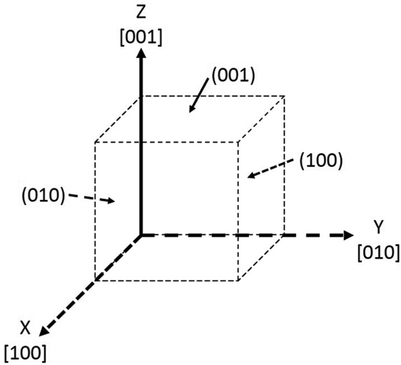
Miller index representation on a cubic system.
Definitions of Miller index notation for plane and direction.
Anisotropy properties of silicon
Location of the primary flat of a (001) silicon wafer is aligned with the [110] direction, with its natural cleavage plane usually running along <110> and <111>. 8 Fracture on silicon is orientation-dependent due to the different bonding forces between each atoms at different directions within the silicon lattice. Mechanical properties such as the Young’s modulus and fracture toughness were also studied to explain the anisotropic fracture behaviour of silicon during machining. Young’s modulus of the silicon can be calculated using equation (1) 9
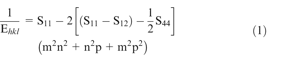
where E is the Young’s modulus; hkl is the three-integer triples corresponding to XYZ axis in a coordinate system; m, n and p are the cosine of angles between direction of interest denoted by [hkl]; S ij is the compliance constant (S11 = 7.68; S12 = −2.14; S44 = 12.6).
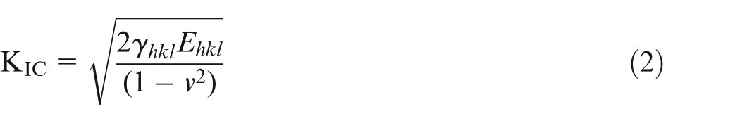
According to equation (1), Young’s modulus is similar on all crystallographic directions for a (111) wafer plane at 188 GPa. However, the Young’s modulus on a (001) wafer plane exhibits a fourfold symmetry behaviour at 169 and 130 GPa along the <110> and <100> directions, respectively. Fracture toughness of silicon, which determines its resistance against crack propagation, is also highly orientation dependent. Using Griffith 10 criterion, fracture toughness at each crystallographic direction can be computed using equation (2)
where
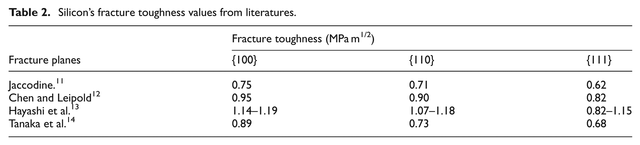
Values of the fracture toughness reported by several articles for {100}, {110} and {111} wafers are shown in Table 2. According to the behaviour of this fracture toughness shown in Table 2, it can be recognized that <100> direction has the highest resistance against crack propagations when compared to <110> and <111>.
Silicon’s fracture toughness values from literatures.
Review on the effect of crystallographic orientation on silicon micromachining
During the early discovery of surface anisotropy on silicon mechanical micromachining, Blackley et al. 3 show that the damages caused by orientation-dependence was contributed by the variation of resolved tensile stress in the {111} slip planes. In addition, relative changes between the machined orientation plane and cutting direction during micro-turning of silicon were also considered in the recent years to explain the machining quality of orientation-dependent silicon surface.
Shibata et al. 15 performed nanoscale ductile mode micro-turning on silicon with crystal surface of (001) and (111). A slip model was used in the qualitative analysis to explain the machined surface effect when turned at different directions. The experiment also shows the anisotropic effect of machined surface taking the form of a fourfold and threefold symmetric across the centre of (001) and (111) wafer, respectively. Hung and Fu 16 studied the effect of crystallographic orientation during ductile mode turning of (100) silicon wafer. The study shows that micro-pitting occurs along <100>, while ductile mode was achieved along <110>.
Cheung 17 had also performed ductile mode micro-turning on (001) and (110) wafers. Surface roughness measured across each crystallographic direction indicates a variation in roughness value when the relative machined surface plane and the cutting directions change during turning. O’Connor et al. 18 show the measurement of critical chip thickness as a function of crystallographic orientation under different cutting conditions and directions on a (001) wafer. Results from the experiments indicate that cutting force measured from dynamometer varies when turned at different directions and ductile mode cutting on (001) wafer can be achieved at a maximum depth of cut of 120 nm in [100] and 40 nm in [110]. Jasinevicius et al. 19 had also showed that the critical chip thickness in ductile material removal mode for (100) silicon wafer reaches a maximum of 285 nm in [100] and 110 nm in [110]. Cracks were also found to be easily formed along <110> when micro-turned at sub-micrometer depth of cut.
Review on the effects of different cutting tools on silicon micro-milling
Coated tungsten carbide (WC) and single crystal diamond tools are commonly used for micromachining of silicon. Rusnaldy et al. 20 had performed a comparative study on micro-milling with TiCN, TiAin and diamond-coated tungsten carbide tools on a (111) silicon wafer. Experiments were conducted in terms of ductile regime machining with an axial depth of cut at 0.3 and 0.5 µm. Results from the investigation show that micro-milling performed with diamond-coated tungsten carbide tool produces the least amount of fracture along the machined surface with a surface roughness measured at 60.7 µm.
Although coating helps to increase resistance against wear and resistance, the thickness of the coatings would increase in cutting edge radius, thereby causing the cutting tool to be blunt. Due to the size effect in microstructure affecting the machining quality of the work-piece, coating on micro-cutting tools might have a negative effect on the micromachining performance. Chemical vapour–deposited (CVD) and single crystal diamond tools possessing exceptional hardness have been introduced for micromachining during the recent years. 21 As the cutting edge radius is in sub-micrometer, the tool cutting edge is considered to be very sharp for micro-cutting processes.
Experimental methodology
Methods for effect of crystallographic orientation on silicon micro-milling
Workpiece and machining equipment setup
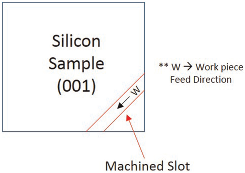
A 15 mm × 15 mm work-piece was cleaved from a (001) silicon with 500 µm and 100 mm in thickness and diameter, respectively, as shown in Figure 2. Micro-milling operations were conducted along <100> and <110> on the (001) surface. Each cutting direction was varied at 45° between 0° and 360°, and the machining conditions are shown in Table 3.
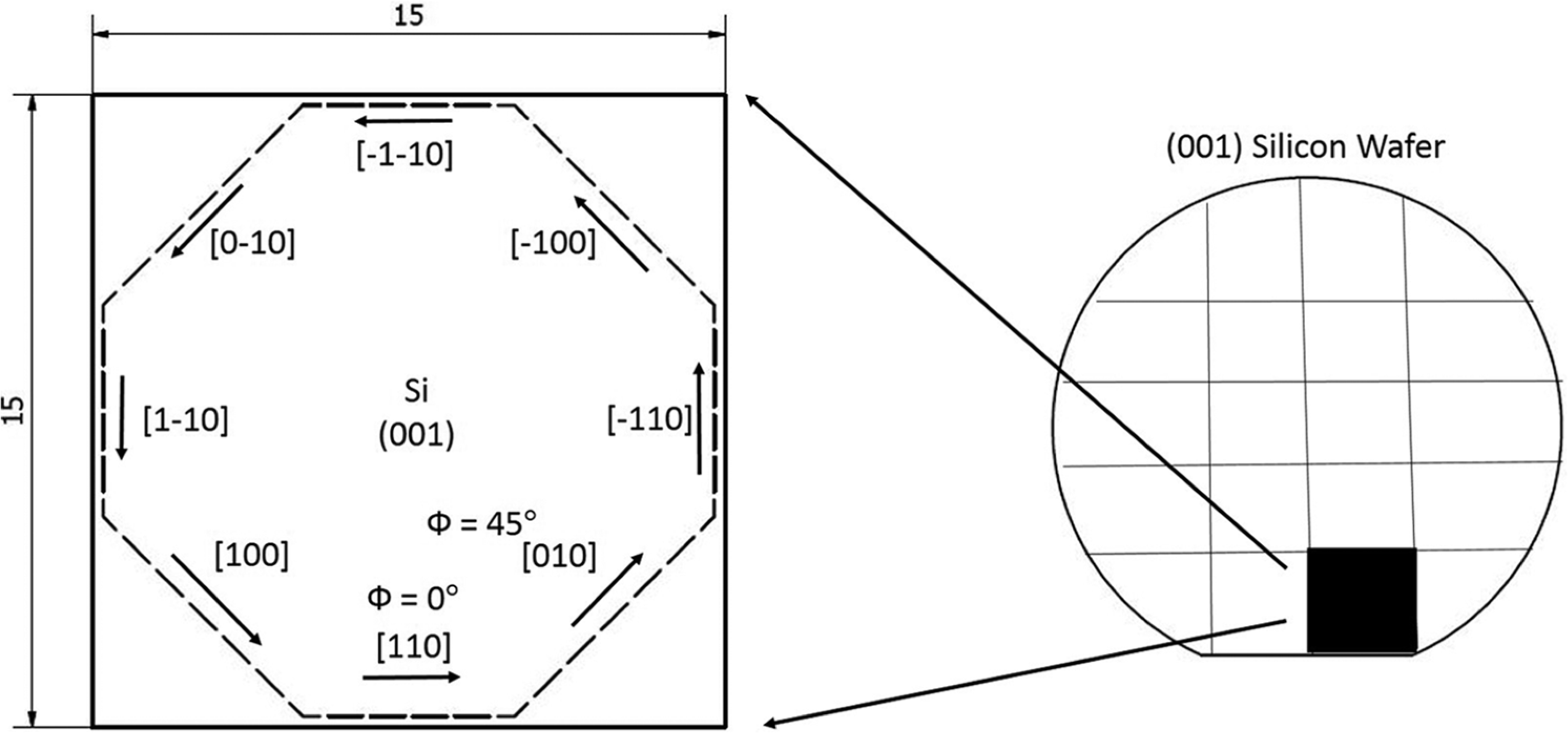
Illustration of silicon work-piece and machining schematic.
Machining conditions for micro-milling operations on a (001) silicon wafer.
The sample was bonded onto a ground metal plate and clamped onto a work-piece holder. Experiment was conducted on Nanowave MTS5R micro-milling system as shown in Figure 3. It consists of a three-axis motion stage, whereby the Y axis actuates the high-speed air-bearing spindle with a 0.5 mm diameter UT coated tungsten carbide end-mill by Air Bearings Ltd and Union Tool Co.. Furthermore, the X and Z axes actuate the work-piece holder and Kistler dynamometer for cutting force measurement during machining.
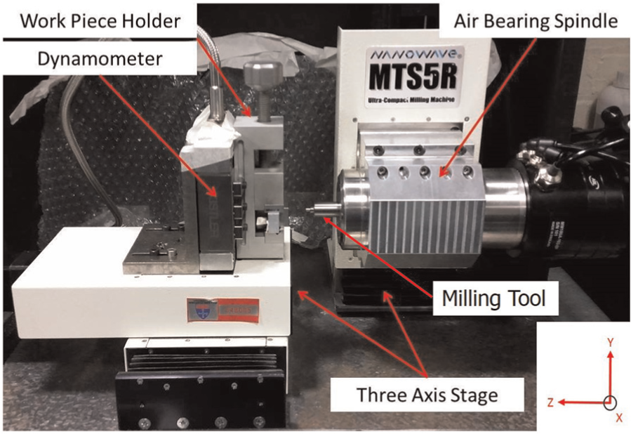
Nanowave MTS5R micro-milling system for performing milling along <100> and <110> directions on a (001) silicon wafer.
Cutting strategy – up-milling
Micro-milling mechanics include two cutting operations, namely, slot and side milling. Furthermore, there are two strategies within side milling comprising either up or down milling. 22 Chip formation in ductile mode occurs when the uncut chip thickness is sufficiently small with the ratio of tool cutting edge radius to uncut chip thickness > 1.
In an up-milling process as shown in Figure 4, the uncut chip thickness begins from a minimum value at the start of cut and approaches a higher value when the cutting tool rotates. This allows minimal material removal at the start of each cut, while its critical chip thickness will only be reached at the later stage. Due to the cutter rotating almost instantaneously along the respective cutting directions, the final machined surface is therefore formed by the exposed surfaces from removed materials in the ductile region during multiple cutting passes. As silicon is brittle, up-milling was applied to ensure minimal damages will be incurred on the final machined surfaces which are aligned with the cutter’s feed direction.
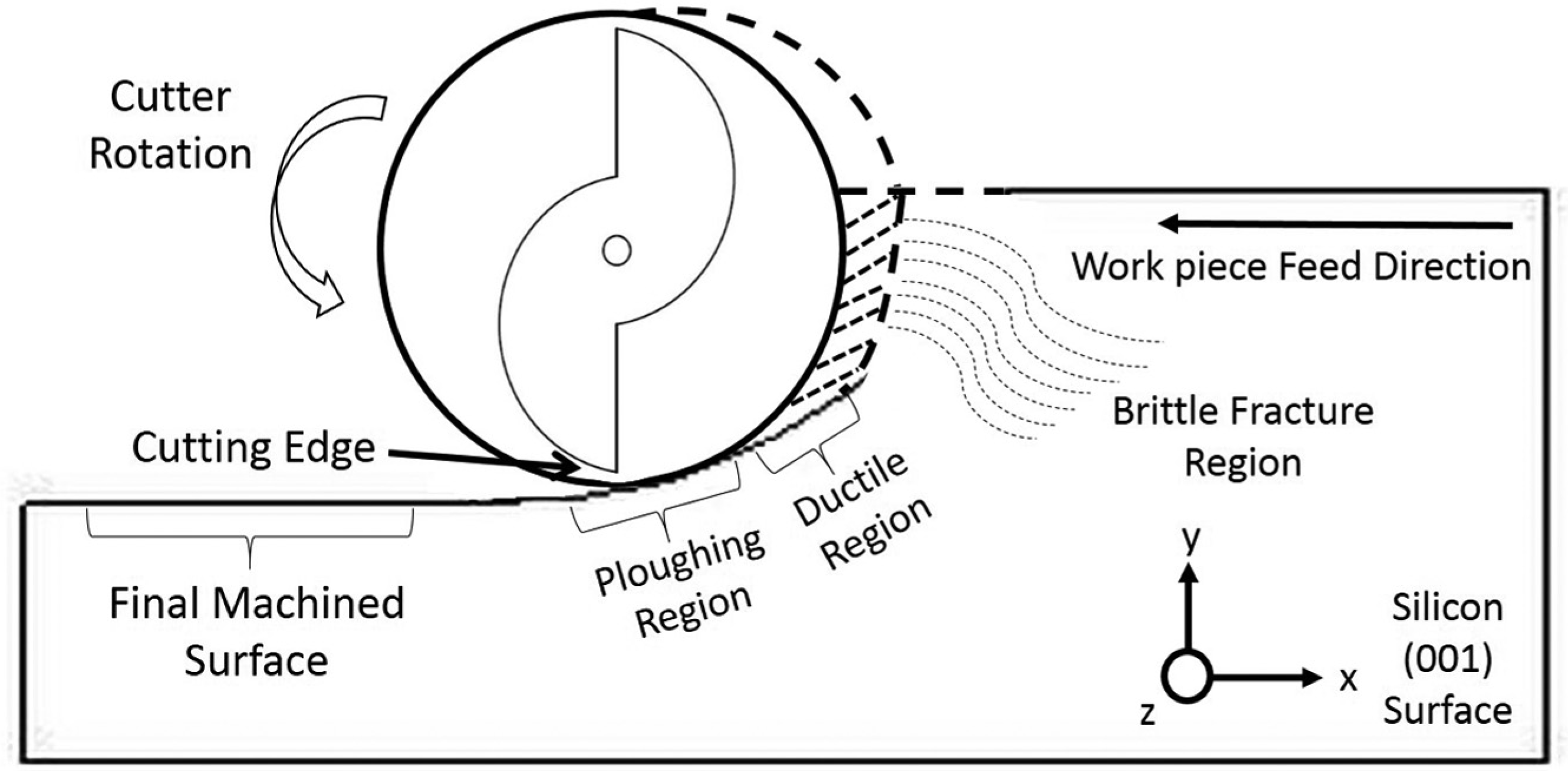
Schematic of up-milling process where the chip thickness begins at minimal and increases towards the end of each cut.
Effect of different cutting tools on silicon micro-milling
Comparative studies on the effect of different cutting tools on silicon micro-milling were conducted using three different end-mills, namely, diamond-coated tungsten carbide tool, CVD diamond tool and single crystal diamond tool. Diameter of each cutting tool was similar at Φ0.5 mm. Figure 5 shows a schematic of the machining plan on the (001) wafer. Table 4 also shows the parameters and profile specifications for machining of each wafer, and the conditions were kept constant throughout each milling operation.
Schematic of machining plan for investigation on the effect of different cutting tools on silicon micro-milling.
Machining conditions for comparative studies on different cutting tools.
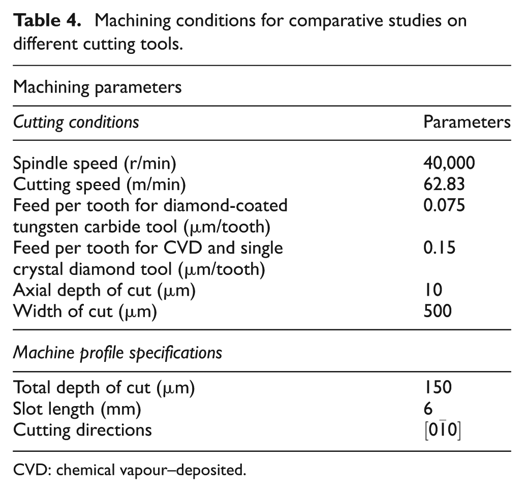
CVD: chemical vapour–deposited.
Results and discussion
Quantitative and qualitative analyses were conducted on the cutting performance of silicon after micro-milling operations. A distinct crystallographic orientation-dependence behaviour was observed. In this section, metrology techniques and the experimental results will be discussed.
Effect of crystallographic orientation during silicon micro-milling
Cutting force analysis
Drift compensation was performed by zeroing all the measured data prior to signal processing. Raw cutting force data were then processed with a second-order low pass filter to remove any high-frequency noises. Ten cycles of cutting force at each cutting directions were obtained for analysis. Finally, the average resultant cutting force at each direction was computed by equation (3)
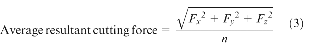
where Fx, Fy and Fz are the processed cutting force at each time point at a specific cutting direction [hkl]; n is the total time point at a specific cutting direction [hkl].
Figure 6 shows the average resultant cutting force of the eight directions as illustrated in Figure 2. Cutting forces measured along <100> direction were significantly larger than those of <110>, thus suggesting greater ductility characteristics along <100>. Such phenomena were expected due to a lower force required to cut the cleavage plane along <110> direction. A fourfold behaviour similar to the silicon cubic crystal structure repeats at every 90°.
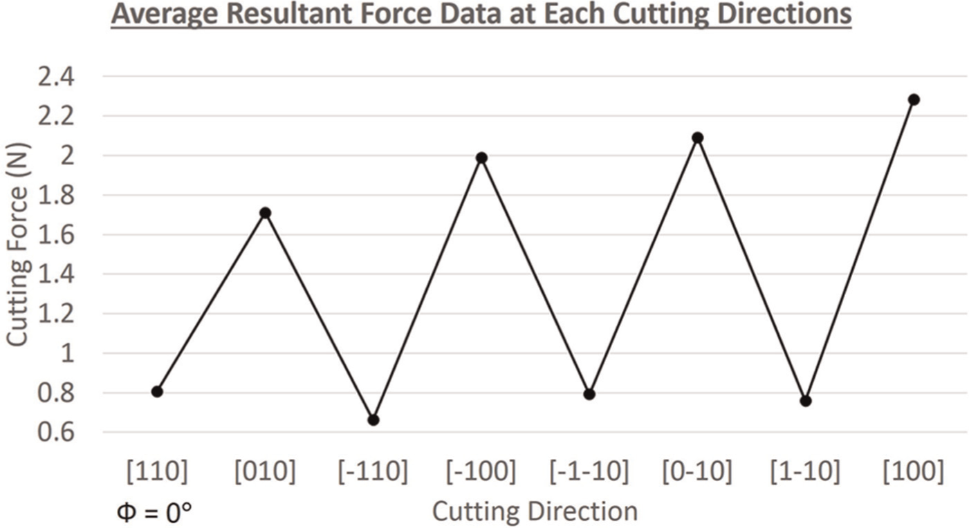
Results of average resultant cutting force at the respective cutting directions.
Analysis on surface roughness and edge chipping
Hitachi TM3030 scanning electron microscope (SEM) system and Zygo NewView 5020 optical surface profiler with 10× objective were used for both edge chipping and surface roughness analysis. Edge chipping was quantitatively characterized by measuring the length of edge chipping illustrated by the schematic shown in Figure 7. Assessment was performed in the middle region of each machined surface along [010] and [110] directions. Average measurement of the length of edge chipping was obtained from 50 equally spaced data points along an approximate length of 220 µm. Figure 8 and Table 5 show the SEM images and quantitative measurements of the respective machined surfaces.
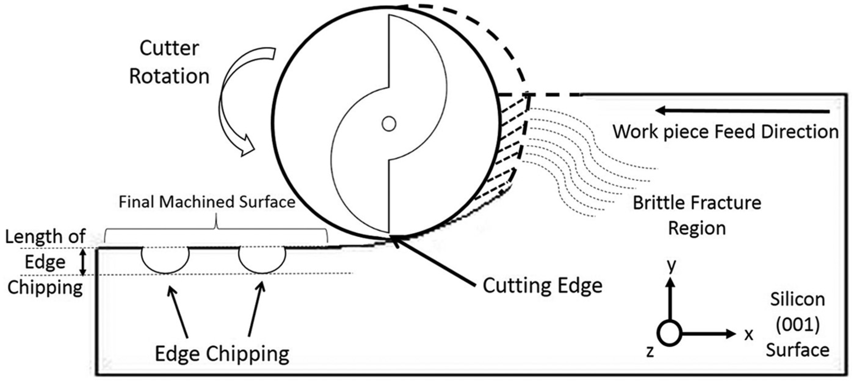
Schematic of micromachined surface with chipping usually formed on the top surface of silicon.
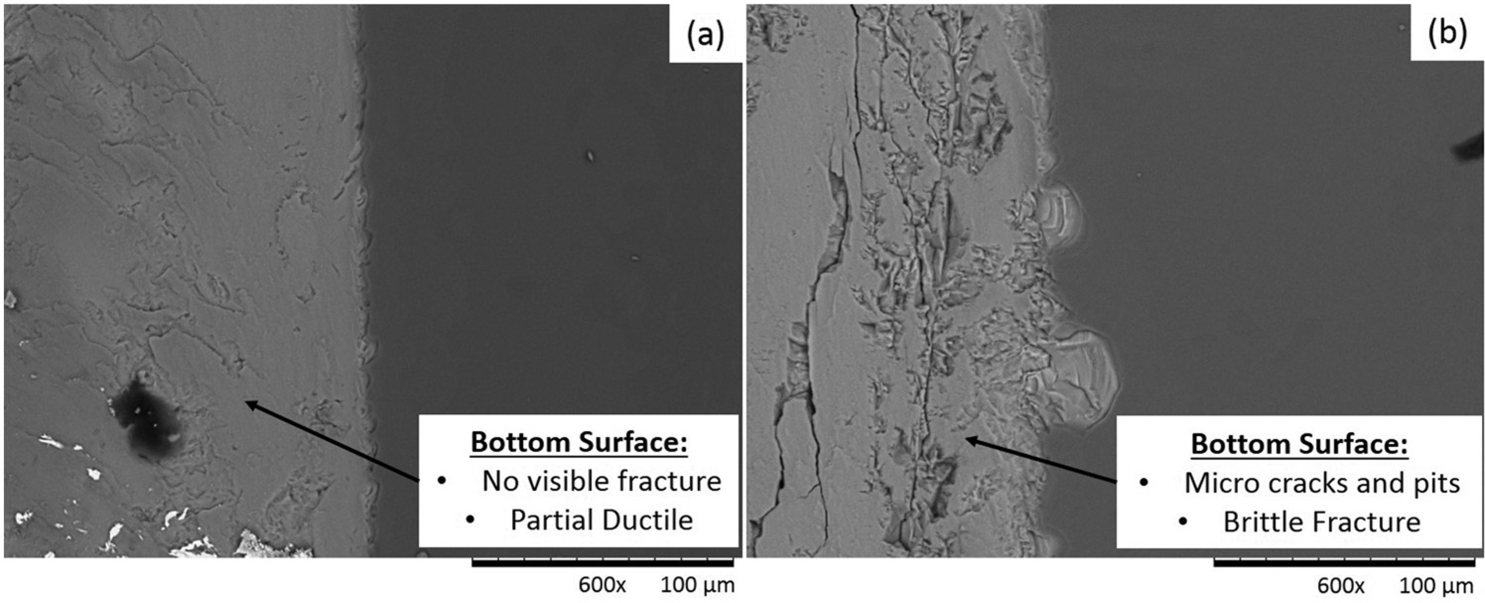
SEM imagery of (a) [010] and (b) [110] machined surfaces.
Surface roughness and edge chipping measurement of [010] and [110] machined surfaces.
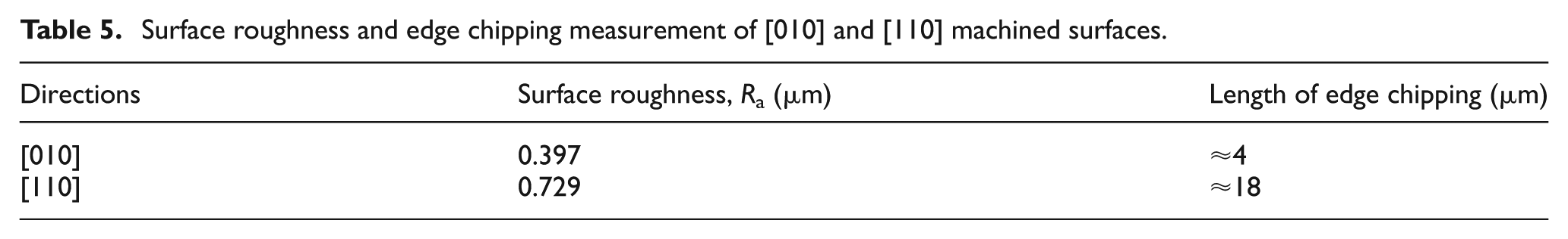
Results from both surface roughness and edge chipping measurement shown in Table 5 were in agreement with the orientation-dependent crack propagation behaviour of silicon. Relationship between fracture toughness of <110> and <100> shown in Table 2 suggests that KIC<100> > KIC<110>. In addition, possible contribution of vibration from the cutting tool causes higher cutting forces to be measured along <100> directions. Vibration causes periodic variation in the actual depth of cut which leads to large ploughing effect on the cutting edge of work-piece and high frictional force. This leads to minor edge chipping and partial ductile quality on the bottom surface as shown in Figure 8(a).
Effect of different cutting tools during silicon micro-milling
Analysis on surface roughness and edge chipping
Slot machining was performed along the
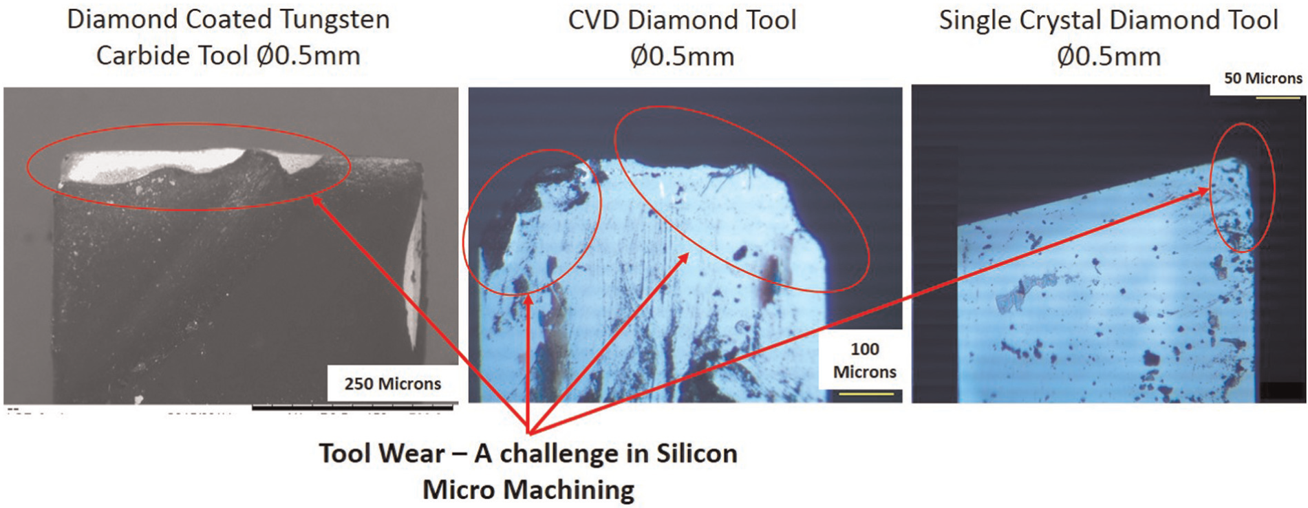
SEM images of tool wear on diamond-coated, CVD and single crystal diamond tools.
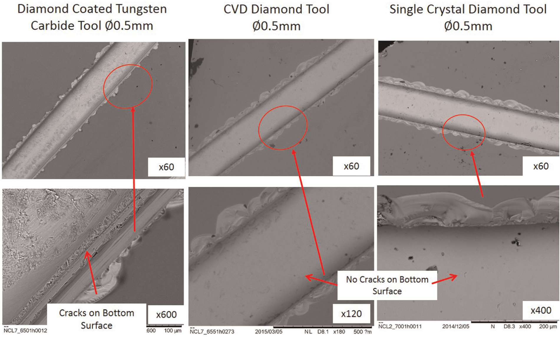
SEM images of machined slot on (001) silicon wafer by diamond-coated, CVD and single crystal diamond tools at ≈150 µm deep.
The bottom surface machined by CVD and single crystal diamond have no visible fracture because both tools have very sharp cutting edges due to the small cutting tool radius. This causes the impact force imposed on the sample surface during contact with the cutting tool to be small. Controversial results on the measured length of the edge chipping shown in Table 6 indicate that single crystal diamond tool generates the largest amount of edge chipping along the
Average and RMS edge chipping length.
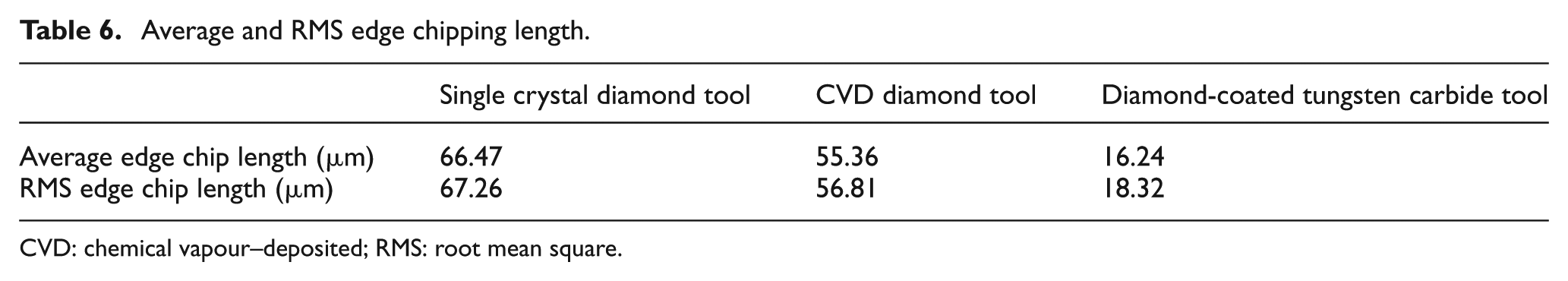
CVD: chemical vapour–deposited; RMS: root mean square.
Large negative rake angle is believed to create highly compressive hydrostatic pressure in the cutting zone, and the highly compressive hydrostatic pressure in turn can suppress the crack propagation. This might be a possible explanation to the large edge chip size generated during micro-milling with CVD or single crystal diamond tool. Although the method proposed to measure the length of edge chipping provides an estimation to quantify edge chipping, more precise method of quantification such as volume measurement of the generated chips should be investigated and applied in the future.
Conclusion
The effect of crystallographic orientation during micro-milling of silicon was investigated and assessed through its cutting performance in this study. Surface roughness and edge chipping measurement indicate that surface quality along <100> was better than that of <110>. Furthermore, cutting forces measured along <110> were lower due to lower fracture toughness and surface energies. This leads to easy dislocation of atoms along <110> direction. Results from the comparative studies of different end-mills show that diamond-coated tool generates the least edge chipping, while single crystal diamond and CVD tools both generate fracture-free bottom surface. Tremendous tool wear on diamond-coated and CVD tools remains a challenge after silicon micro-milling operations.
This research is in agreement with previous studies as a significant presence of crystallographic orientation effect affecting the quality of machined silicon by micro-milling. Furthermore, results from this research had demonstrated that by machining silicon along <100> directions, partial fracture-free machining quality was achieved. However, in conjunction with previous studies, it was recognized that fracture-free machining quality for brittle materials cannot solely depend on mechanical micromachining. Generation of edge chipping remains a challenge even if machining was conducted along <100> directions. Future perspectives to develop mitigating strategies for such challenge would include the introduction of protection techniques to the silicon to minimize edge chipping.
Footnotes
Declaration of conflicting interests
The author(s) declared no potential conflicts of interest with respect to the research, authorship and/or publication of this article.
Funding
The authors disclosed receipt of the following financial support for the research, authorship, and/or publication of this article: The authors wish to thank EPSRC (EP/M020657/1) and Newcastle University SAgE Doctoral Training Award scheme for supporting this work. The authors are also grateful to Air Bearings Ltd for providing the high-speed air bearing spindles which were used in the experiments.