
Abstract
Binding of metal powders using electrochemically deposited binders provides a novel approach to achieve metal additive manufacturing at ambient temperature. In this study, using an in-house built experimental setup, a single layer of copper powders were electrochemically bound together with the help of nickel binder and the deposits were studied by scanning electron microscope and energy-dispersive X-ray spectroscopy. Mechanical characterization performed on the deposits reveals that the yield strength of the deposit is comparable to that of laser-sintered parts made from Cu/Ni powder. Furthermore, Taguchi studies have been conducted to investigate the optimal process parameters required for minimum diameter of electrochemically bound spot, layer thickness and yield strength. Analysis of variance and signal-to-noise ratio were used to determine the important levels of process parameters and the results were then experimentally verified.
Keywords
Introduction
The demand for microproducts is ever increasing due to its application in a wide range of industries. 1 These microproducts are often required to be made of wide range of materials and have potential applications in varied industries including medical, automotive, optics, biotechnology and electronics sectors. To meet this demand for multi-material micromanufacturing, it is essential for continuous improvement in micro- and nanofabrication technologies. 2 There exists a broad range of microfabrication technologies each having its own capabilities, applications and limitations. Numerous classification systems are used to classify microfabrication techniques.1,3,4 Most of the microfabrication techniques are restricted when it comes to fabricating microproducts with diverse materials and complex three-dimensional (3D) microstructures with high aspect ratios. 5 Nevertheless, there have been some recent improvements in the micromanufacturing of 3D microstructures using different methods and materials. 6 Some of these improvements include methods such as soft lithography, 7 laser photoablation, 8 localized electrochemical deposition (LECD), 9 lithography, electroplating, and molding (LIGA) process10,11 and electrochemical fabrication (EFAB). 12 Most of the above processes were developed for 2.5D micromanufacturing and hence are not suitable for producing a real 3D micro part. Recently, micro additive manufacturing (AM) based on layer-by-layer manufacturing has been considered as an effective process that can manufacture true 3D microproducts.13,14
3D micro-AM is grouped into scalable AM processes—works at both the macro- and micro scales; 3D direct writing (3DDW)—works at the microscale and hybrid processes which are a combination of these two approaches. 14 Micro stereolithography (MSL) is a process developed by 3D Systems, Inc. and uses ultraviolet light to conduct layer-by-layer photo-sensitive resin polymerization. 15 MSL can produce microparts with 1–10 μm layer thickness and is used in areas such as micromachines and microsensors. 16 MSL processes still have a limitation of not fabricating a wider range of materials. In selective laser sintering (SLS), a high-temperature laser sinters layers of very fine powder. After each layer is sintered, a roller is used to spread a fresh layer of powder and the process is repeated.17,18 Selective micro laser sintering, a variant of SLS for micromanufacturing, needs to be performed in a vacuum chamber to avoid humidity and resulting oxidation.19,20 Furthermore, there are limitations with respect to powder handling, part removal and surface roughness. Since it is a thermal process, there are consequent limitations with respect to thermal damage of the part. For the selective laser melting process, yet another AM method is limited by the non-availability of specialized systems that can do micro manufacturing. 21 Inkjet printing is another AM process that employs layer-by-layer deposition of a liquid material in droplet form. 22 The material then turns into solid by cooling, chemical changes or solvent evaporation. A major limitation is the need of support structures for complex micro features. Also the removal of these support structures after the part is machined is a problem. 23 One of the problems of inkjet process is that the fluid which acts as the binder is ejected through a nozzle. The diameter of the orifice is usually less than 100 μm. Hence, the binder should have low viscosity and high stability to prevent orifice clogging.24,25 Also, the jetting process must be performed in a low-oxygen environment to prevent the formation of a surface oxide layer, thus resulting in changes to the physical properties of the jet surface.26,27 To overcome the existing limitations such as thermal damage, orifice clogging and support structures, a novel metal AM at room temperature by electrochemical deposition is being developed. 28 In this connection, in this article, the feasibility of binding metal powders using electrochemically deposited binders is studied to enable metal AM at ambient temperature.
Principle of binding of metal powders by electrochemical deposition
The process studied in this research combines the principles of 3D printing and LECD to present a novel micro-AM technique. In this feasibility study, a single layer of copper powder is spread on a substrate immersed in an electrolyte bath and the tip of an electrode is brought near it. Electric field is passed to perform electrolysis. Nickel from the electrolyte is deposited locally below the tip of the micro anode. This results in the copper powder located below the electrode to be electrochemically bound by the nickel deposit which acts as a binder.
The reactions taking place at the anode and cathode are shown as follows


A schematic of the process is shown in Figure 1.
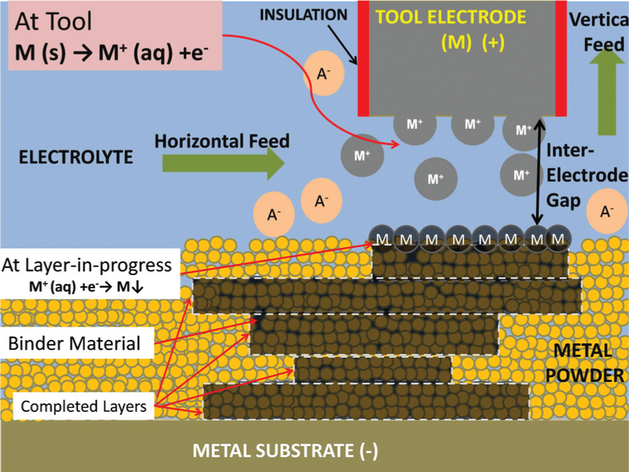
Schematic of binding process.
Experimentation
Experimental setup
The in-house built experimental setup for the process, shown in Figure 2, consists of a three-axis computer numerical control (CNC) stage and controller. An electrolyte tank fitted on top of the stage serves as the machining chamber. The movement of the axes of the stage is handled by three individual NEMA 08 stepper motors. The stage is connected to low-current stepper motor controllers which are in turn connected to a parallel port breakout board. This breakout board connects to the PC and acts as a liaison between the stage and the PC-based controller. Mach3, a PC-based controller, is used to control the movement of the axes of the stage. It takes in G codes and sends out step/direction pulses based on the G codes to control the movement of the stage. The axes of the stage can travel a maximum of 10 mm. The minimum movement of each axis is 1 μm. The feed rate is user defined and can range from a high of 32 mm/min to a low of about 1 μm/s. There is a spindle mounted over the electrolyte tank which houses the tool required for the machining process. The spindle is controlled by Mach3 and can be used to rotate the tool at a programmed speed.
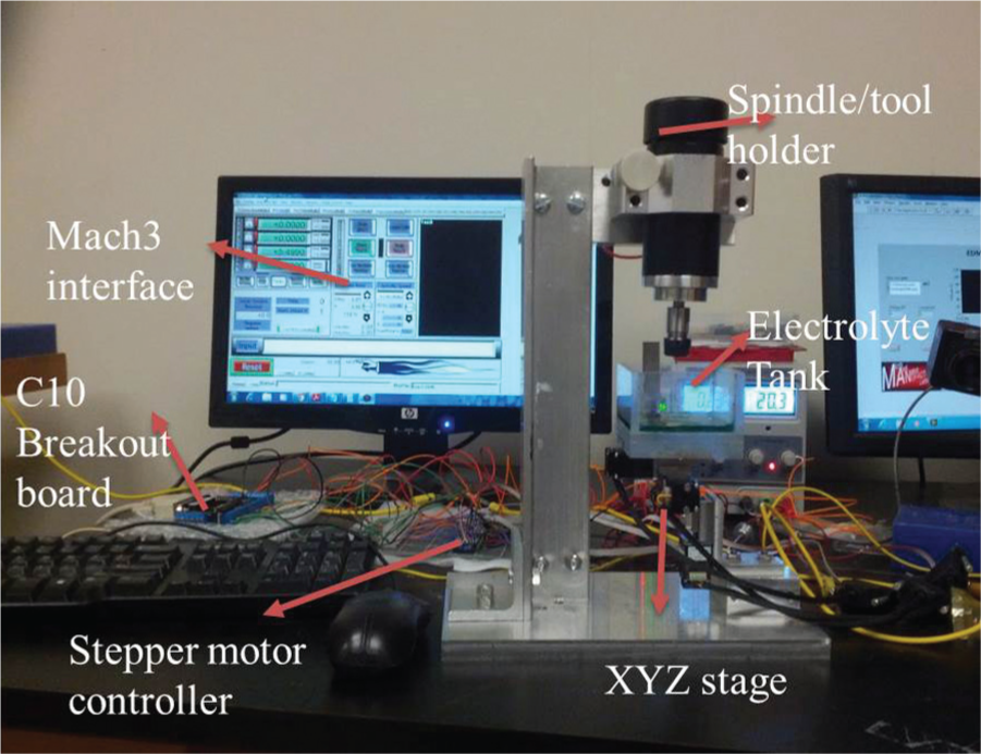
In-house built experimental setup.
Experimental detail
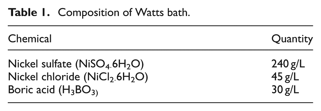
A platinum tool of 250 μm diameter was used as the anode. The tool was coated on the sides with an insulating material with only the tip exposed. Copper and brass plates were used as the substrate (cathode). The substrates were fine polished using different size sandpapers to get a smooth uniform finish. The substrates were then washed with deionized water and cleaned in an acetone ultrasonic bath for 3 min to rid it off any surface contaminants that might be presented. The literature suggests that powders having a grit size of more than 25 μm are suitable for both dry and wet deposition methods. 29 Therefore, in this study, copper powder of size 44 μm was used for the experiments. The substrate along with the copper powder was placed inside the electrolyte cell. A pulsed power supply was chosen for this process to achieve localized deposition. The composition of the electrolyte (Watts bath) is listed in Table 1. The initial experimental parameters used to study the feasibility are listed in Table 2.
Composition of Watts bath.
Experimental parameters.
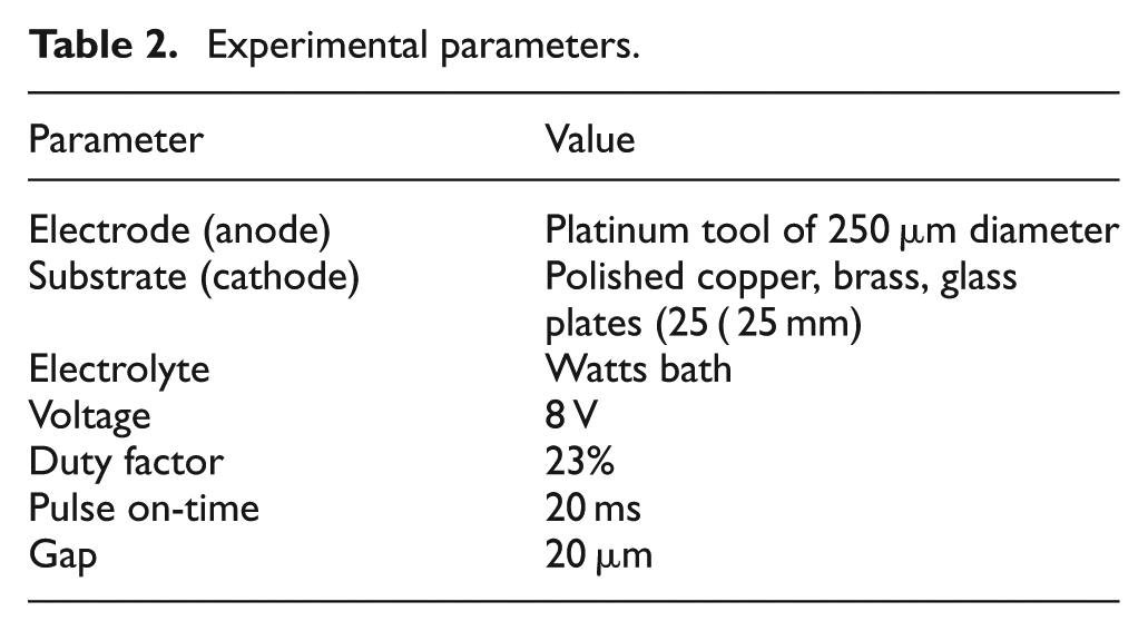
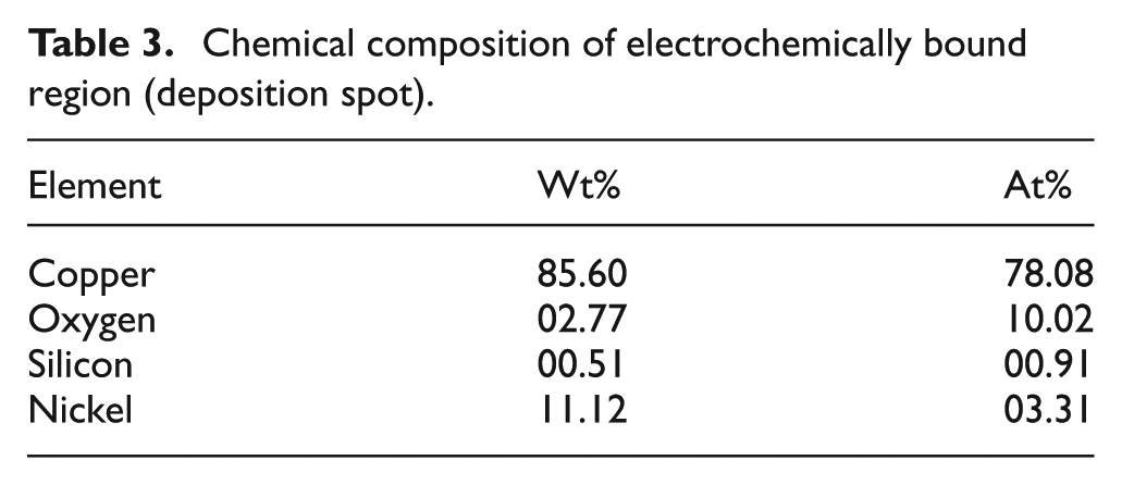
Figure 3 shows the binding of copper powders by nickel deposition. Energy-dispersive X-ray spectroscopy (EDX) results for the deposition spot can be seen in Figure 4 along with the chemical composition in Table 3.
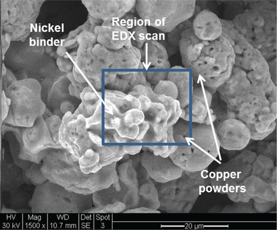
Copper powder electrochemically bound by nickel binder.
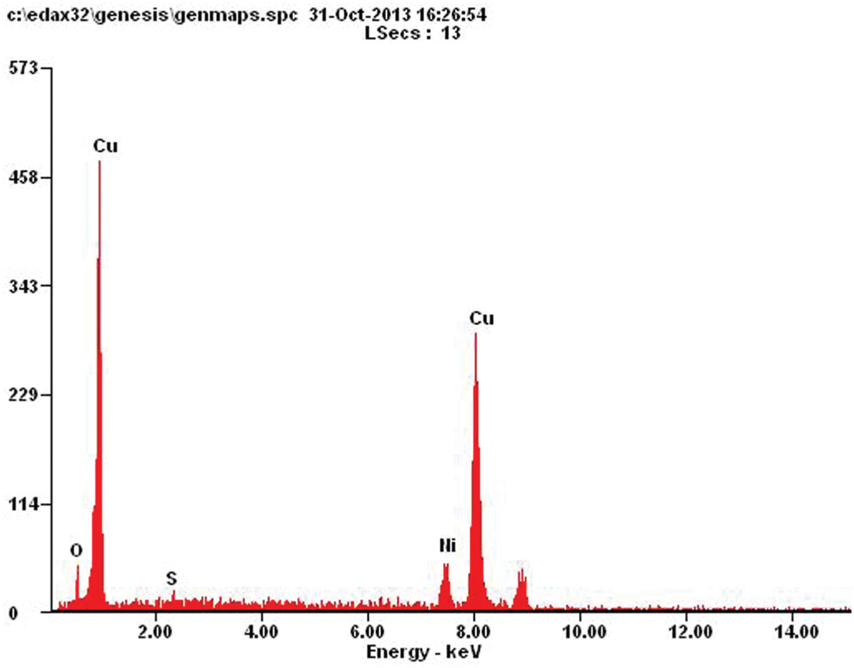
EDX of the electrochemically bound spot showing the presence of nickel binder and the copper powders.
Chemical composition of electrochemically bound region (deposition spot).
The amount of nickel binder present on the deposition spot depends on the time for which the deposition experiments are carried out. In traditional 3D printing, the binder material used is always significantly lesser than the amount of powder to be bound. During the experiments, it was found that carrying the deposition for 20 s gave the ideal amount of binder needed to bind the required amount of copper. Hence, there is a relatively lower amount of nickel at the deposition spot on the EDX results. Figure 5 shows X-ray diffraction analysis data of the deposition spot. This further corroborates the role of nickel acting as a binder during the process.
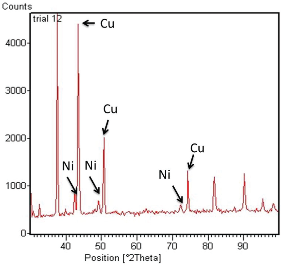
XRD analysis graph of the deposition spot.
Results and discussion
After the feasibility of the idea was established, experiments were carried out to optimize the process parameters which would give smallest diameter of deposition and minimum layer thickness of deposition.
Diameter of deposition spot
In a traditional 3D printing system, the diameter of the nozzle tip gives the diameter of the binding spot. This information helps in programming the system such that one pass of the nozzle will bind a certain area of the powders. Consequently, based on the area of the part, the number of passes of the nozzle is set and the process is run.
But in the case of the process proposed in this article, the binder is generated through LECD. Ideally, in LECD, the diameter of deposition must be as close to the diameter of the tool being used. 30 This means that each pass of the tool should glue an area proportional to the diameter of the tool. But the actual diameter of deposition is dependent on the process parameters being used and varies with respect to that. Hence, the diameter of deposition spot is considered as an output parameter and studied with respect to the input parameters to better control the process and be advantageous in gluing true 3D parts together.
Height of deposition
The height of deposition is the same as the layer thickness of each layer in a traditional 3D printing process. All 3D printers have a setting wherein layer thickness values can be set depending on the part to be printed. 31 The thickness of the layer plays a vital role in the strength and surface finish of the part.14,32 In the process proposed in the article, the binder is being generated through electrochemical reactions, and hence there is a need to find the process parameters which give minimum amount of binder generated thereby having better control over the process.
Taguchi methodology for design of experiments
Taguchi methodology was used to find out the influence of the process parameters on the selected outputs. Taguchi uses two important tools, namely, orthogonal arrays and signal-to-noise (S/N) ratios. 33 Orthogonal arrays help in conducting minimal number of experiments while still giving full information of all the factors affecting the output. S/N ratios give an indication of the effect of changing one process parameter on the entire process. 34
Taguchi methodology uses three quality characteristics, namely, smaller-the-better, nominal-the best and larger-the-better. 35 In this study, our objective was to reduce the diameter of deposition and get a minimum layer thickness of binder deposited. Hence, we have used the smaller-the-better quality characteristic in this study.
Selection of process parameters
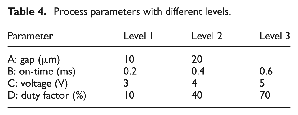
Numerous experiments were conducted to narrow down on process parameters and their levels. It was found that gap (A), on-time (B), voltage (C) and duty factor (D) had the most influence on the diameter and height of deposition. The ideal voltage lay between 3 and 5 V, and hence, 3, 4 and 5 V were selected as the levels of this parameter. It can be seen from the literature that a smaller on-time gives a localized deposition when compared to higher on-times. Hence, on-times of 0.2, 0.4 and 0.6 ms were used as the levels. The gap between the electrodes was set at 10 and 20 μm. Duty factor expresses the time duration for which the current assumes a non-zero value in a cycle. It is given as a percentage, that is,
Process parameters with different levels.
Selection of orthogonal array
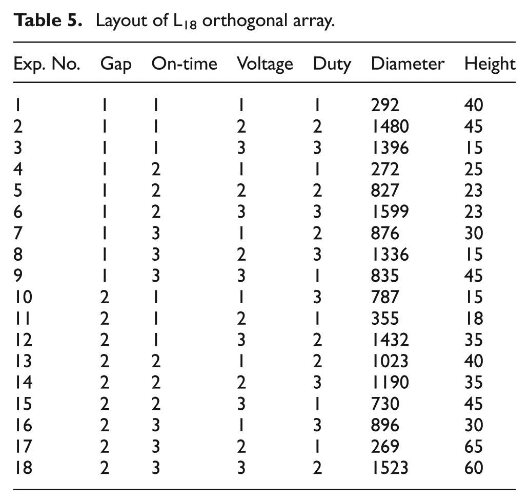
The selection of the orthogonal array depends on the total number of degrees of freedom (DOFs) of the process parameters. 36 DOF is defined as the number of comparisons that need to be made to determine the ideal level. 37 In this study, there are three parameters having three levels each and one parameter has two levels. Hence, the total number of DOFs is 7. The orthogonal array selected must have an equal or greater number of DOFs. 35 This study uses the L18 orthogonal array. Table 5 shows the layout of the L18 orthogonal array.
Layout of L18 orthogonal array.
Analysis
Output parameter 1—diameter of deposition spot
An optical microscope was used to determine the diameter of deposition spot.
For smaller-the-better quality characteristic, the S/N ratio was calculated using
where yu is the mean response value, u is the trial number, i is the experiment number and Ni is the number of trials for experiment I.33,36
Analysis of variance (ANOVA) was carried out at 95% confidence level. ANOVA results are given in Table 6.
ANOVA for diameter of deposition spot.
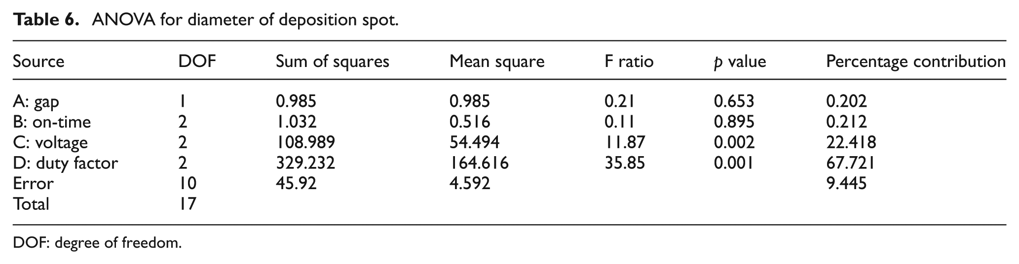
DOF: degree of freedom.
The p value and F ratio indicate the statistical significance of each factor. The p value is less than 0.05 for both voltage and duty factor. This indicates that these factors have a statistically significant impact on the diameter of deposition at 95% confidence level. This is consistent with what was observed during the experiments. A higher voltage coupled with a high duty factor resulted in a very large deposition area with vigorous bubbling which would invariably disperse the copper powder. A relatively lower voltage and duty factor gave a controlled deposition spot with minimum dispersion of copper powder due to bubbling. The F ratio is more than 4.5 for both voltage and duty factor. This indicates that the response variable (diameter) changes significantly with variation in the levels of voltage and duty factor in the range of selected levels.
The S/N ratio is given in Table 7. The ratios reveal that a gap of 20 μm (Level 2), on-time of 0.2 ms (Level 1), voltage of 3 V (Level 1) and a duty factor of 10% (Level 1) are the optimum parameters for a highly localized deposition spot. As explained earlier, a lower voltage and duty factor help in getting a highly localized deposition spot with the smallest diameter.
S/N ratio for diameter of deposition spot.
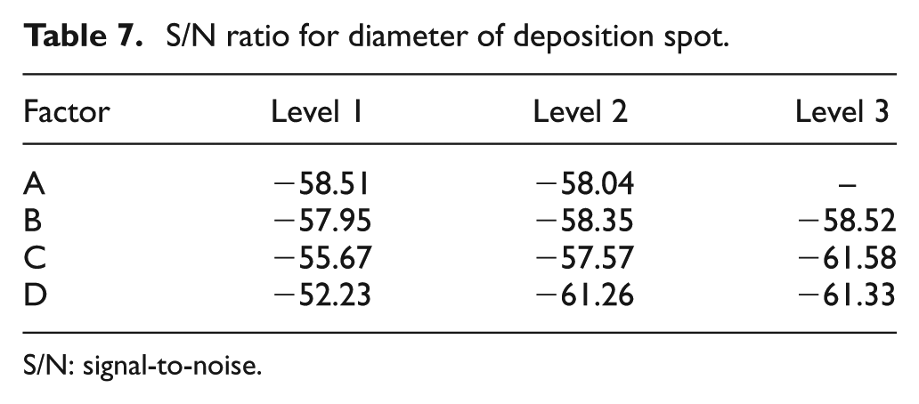
S/N: signal-to-noise.
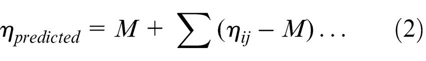
Confirmation experiments were done to verify the analysis results. The optimum value of diameter of deposition spot was computed as
where M is the overall mean of diameter of deposition and
Confirmation experiments.
Output parameter 2—height of deposition
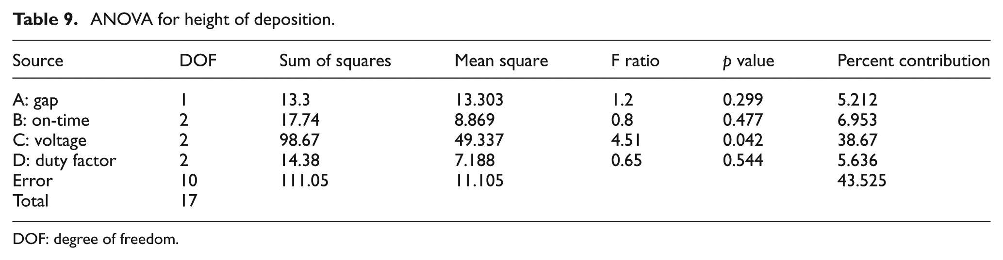
A commercially available Mitutoyo Surftest SJ-410 Series was used to measure the height of deposition. Smaller-the-better quality characteristic was used to calculate the S/N ratios. ANOVA was performed to find out the significant parameters at 95% confidence levels (Table 9). Data points were obtained from the profilometer which were then plotted using MATLAB to get graphs depicting the heights of deposition (Figures 6 and 7).
ANOVA for height of deposition.
DOF: degree of freedom.
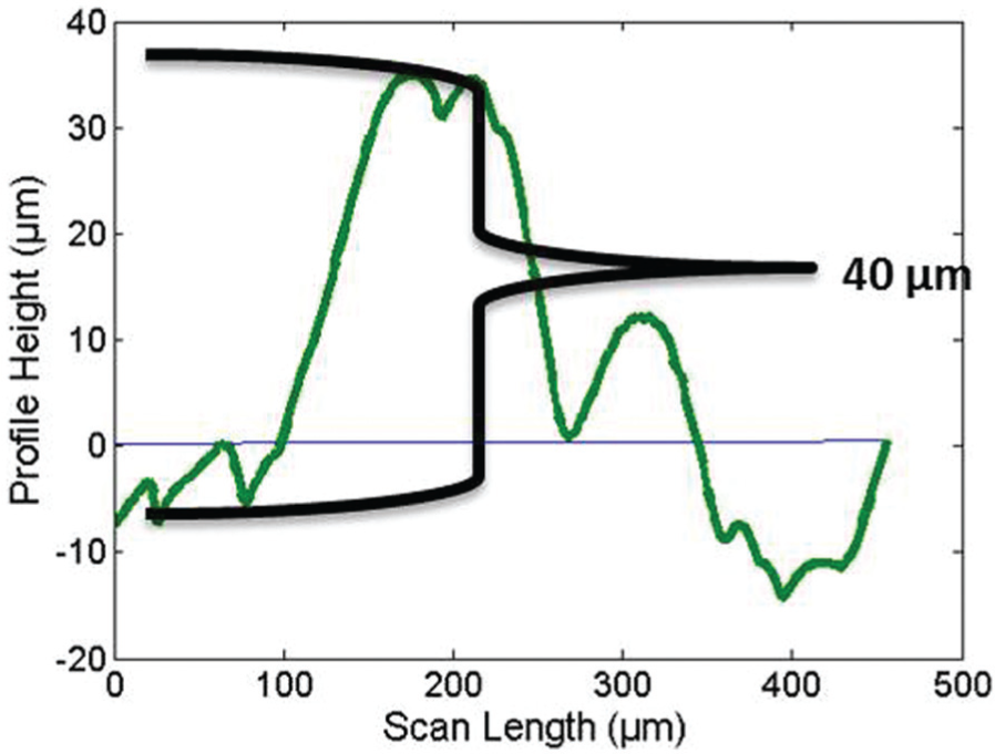
Height of deposition (Exp. No. 1).
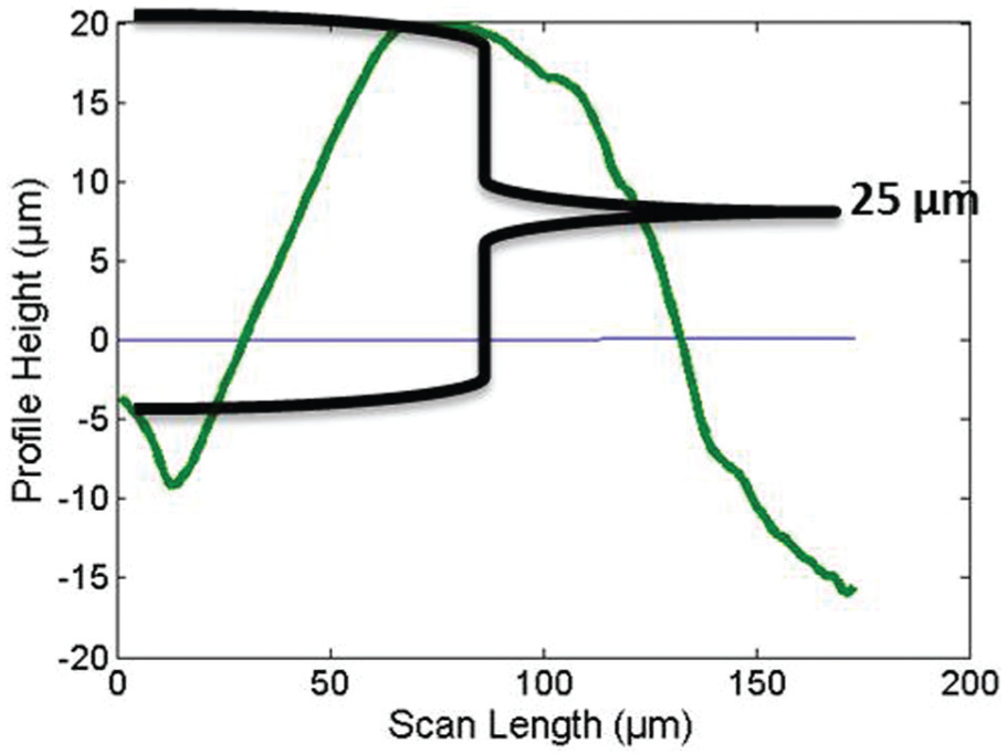
Height of deposition (Exp. No. 4).
The p value and F ratio indicate the statistical significance of each factor. The p value is less than 0.05 for voltage. This indicates that this factor has a statistically significant impact on the height of deposition at 95% confidence level. The F ratio is more than 4.5 for voltage. This indicates that the response variable (height of deposition) changes significantly with variation in the levels of voltage in the range of selected levels. Higher voltage gave vigorous bubbling and hence dispersed the copper powder at the deposition spot, thus affecting the thickness of deposition. Too low a voltage and there was little deposition which also affected the height of deposition. Duty factor of the pulse power affects the porosity and surface finish of the deposited structure. It is found that lower duty factors result in lesser pores and a smoother or controlled finish. This is explained by the mass transport of the ions during the off-time resulting in the replenishment of the ions. 38 Hence, it is found that duty factor is a significant factor in the study of diameter of deposition spot since this correlates closely with a smoother or controlled finish. However, since the height of deposition does not take into account the surface finish or the porosity of the deposit, it was found that duty factor was not significant in this study.
The S/N ratio is given in Table 10. The ratios reveal that a gap of 10 μm (Level 1), on-time of 0.2 ms (Level 1), voltage of 4 V (Level 2) and a duty factor of 70% (Level 3) are the optimum parameters to obtain minimum height of deposition.
S/N ratio width of deposition.
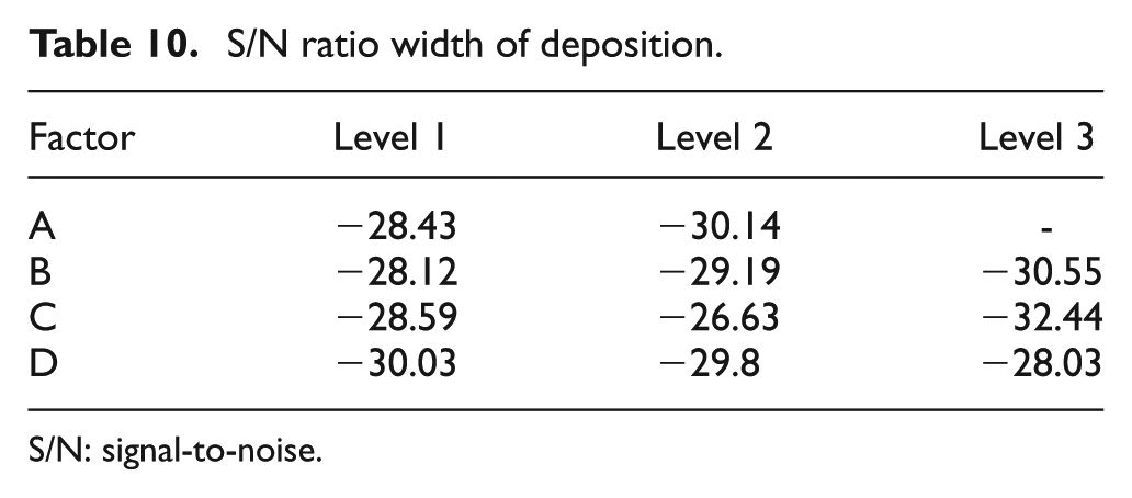
S/N: signal-to-noise.
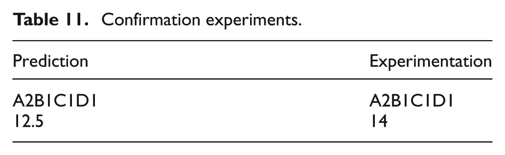
Confirmation experiments were done to verify the analysis results. The experimented and predicted values for diameter of deposition are shown in Table 11. The experimented values were found to be within 11.5% of the predicted value.
Confirmation experiments.
Yield strength study of the electrochemically bound part
The binding strength of the sample deals with the yield strength of the electrochemically bound part. Though 3D printing can print parts of complex shapes and sizes, the parts are usually flimsy, hence deforming under stress. Therefore, the strength of the part is an important parameter that needs to be studied. Hence, a detailed yield strength study was carried out by varying the process parameters and studying how they change the strength of the samples.
Characterization studies were performed on the electrochemically bound part to find out its yield strength. A CSM nanoindentation tester (NHT) was used to carry out the tests. The tester gave a hardness value in the form of a Vickers Hardness number (HV). The HV number was correlated to get approximated yield strength values using the following relationship
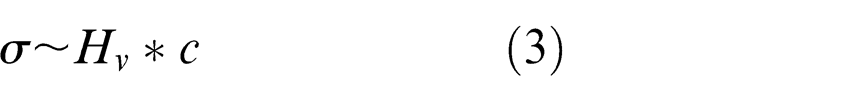
where σ is the yield strength of the bound part (MPa), c = 3.33 and Hv is the Vickers hardness.
For the study, three replicates were performed for a total of 18 × 3 = 54 experiments. The first set of 18 experiments was performed and the yield strength values were measured. Larger-the-better quality characteristic was chosen as the aim was to maximize the yield strength of the electrochemically bound part.
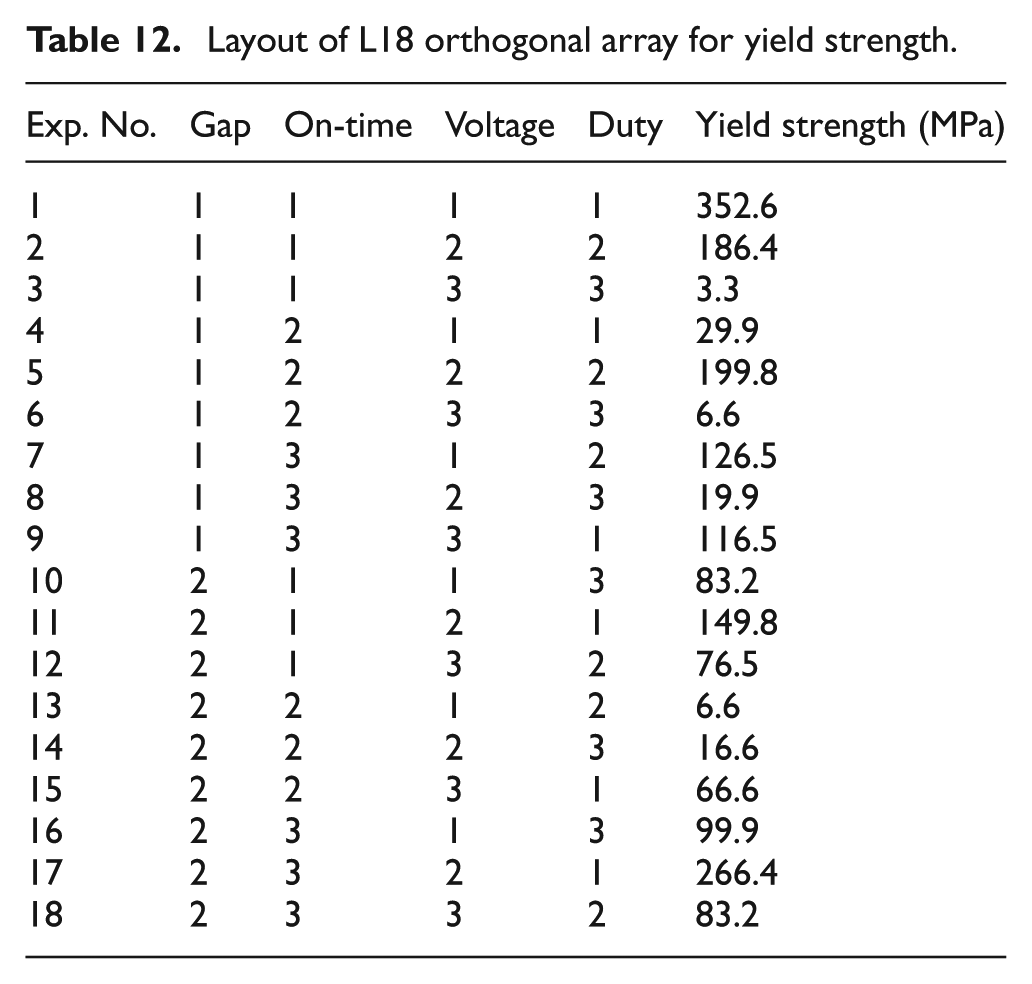
For the first set of experiments, Taguchi and ANOVA analyses did not yield any significant factors which would affect the yield strength. Another set of 18 experiments were performed using the same input factors and the yield strength value was measured. Taguchi and ANOVA analyses were performed again. This trial showed that duty factor was a significant factor at 95% confidence level. The experiment was repeated for a third time with the same input factors. Again Taguchi and ANOVA analyses yielded duty factor to be significant. The yield strength values obtained during the second and third trials were more or less similar. The yield strength values for the third trial are shown in Table 12. The yield strength values measured on the electrochemically bound part were similar to the values of laser-sintered parts made using Cu/Ni powder. 13
Layout of L18 orthogonal array for yield strength.
ANOVA results are given in Table 13. The p value and F ratio indicate the statistical significance of each factor. The p value is less than 0.05 for duty factor. This indicates that this factor has a statistically significant impact on the yield strength of the electrochemically bound part at 95% confidence level. The F ratio is more than 4.5 for duty factor. This indicates that the response variable (yield strength) changes significantly with variation in the levels of duty factor in the range of selected levels. A higher duty factor results in a rough deposit having a loose structure. The deposit appears as an aggregate of loose powders. This adversely affects the yield strength of the electrochemically bound part. This is in accordance with the literature on LECD which shows that high duty factors tend to give loose deposits. 38 Also a higher duty factor results in a very large deposition area with vigorous bubbling, which would invariably disperse the copper powder. This tends to affect the yield strength of the electrochemically bound part.
ANOVA for yield strength.
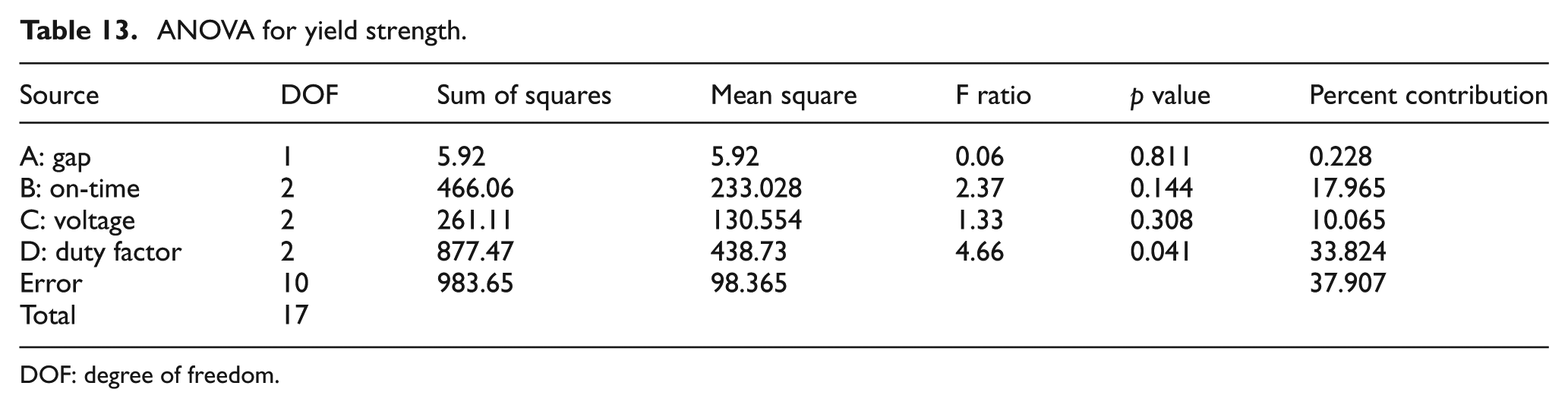
DOF: degree of freedom.
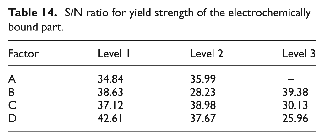
The S/N ratio is given in Table 14. The ratios reveal that a gap of 20 μm (Level 2), on-time of 0.6 ms (Level 3), voltage of 4 V (Level 2) and a duty factor of 10% (Level 1) are the optimum parameters for maximum yield strength of the bound part. As mentioned earlier, a low duty factor with medium voltage gives the bound part which has the best yield strength value.
S/N ratio for yield strength of the electrochemically bound part.
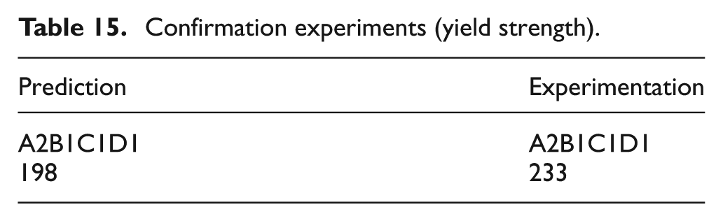
Confirmation experiments
It is noted that the optimal combination of parameters, that is, gap of 20 μm (Level 2), on-time of 0.6 ms (Level 3), voltage of 4 V (Level 2) and a duty factor of 10% (Level 1) coincidentally matches with one of the experiments in the orthogonal array (Trial 17). Hence, no confirmation experiments are needed to verify the design.36,39 Confirmation experiments were still carried out to verify the analysis results. The experimented and predicted values for yield strength are shown in Table 15.
Confirmation experiments (yield strength).
Conclusion
Taguchi method–based experimental design was used in this work to study the binding of copper powders with electrochemically deposited nickel binder and the following conclusions were drawn:
Voltage and duty factor were found to have the maximum influence on the diameter of deposition and in turn the diameter of copper powder bound.
The validation results confirmed that shorter pulse on-time with low voltage and duty factor coupled with a higher inter-electrode gap gave the smallest diameter of deposition and hence the smallest diameter of bound metal powders.
Voltage was found to have the maximum influence on the height or layer thickness of deposition.
The validation results confirmed that shorter pulse on-time with high duty factor and medium voltage coupled with a smaller inter-electrode gap gave a minimum height or layer thickness of deposition.
Duty factor was found to be the most significant factor influencing the yield strength of deposition.
The validation results confirmed that a longer pulse on-time with medium voltage and a low duty factor value coupled with a high inter-electrode gap gave the best yield strength values in the electrochemically bound part.
Footnotes
Appendix 1
Declaration of conflicting interests
The author(s) declared no potential conflicts of interest with respect to the research, authorship, and/or publication of this article.
Funding
The author(s) disclosed receipt of the following financial support for the research, authorship, and/or publication of this article: This material is based on the work supported by the National Science Foundation under Grant No. CMMI-1400800.