
Abstract
In this article, quality analysis of the assembled phase-only liquid crystal on silicon devices is presented based on experiences using the flexibility and scalability of die-level assembly process. The research contents mainly consist of quality control and optimisation of liquid crystal filling process and device overall quality assessment including the thickness uniformity of liquid crystal layer with post-assembly inspection. To summarise, pre-production prototype phase-only liquid crystal on silicon devices with high quality has been developed in high reproducibility using a die-level assembly process, the robust glue deposition is performed, liquid crystal filling process in isotropic phase is presented and thickness variation can be controlled in the range of λ/4.
Introduction
Liquid crystal on silicon (LCOS) devices assembly technology has been considered previously for ferroelectric LC devices 1 and nematic LC devices. 2 Commercial amplitude modulating LCOS devices utilise wafer-level assembly techniques 1 adapted from established liquid crystal display (LCD) 3 high-volume production lines. For instance, the successful JVC D-ILA projectors use the VAN mode LCOS devices produced by wafer-level assembly process. 4 The wafer-level approach assembles large size glass panels on whole silicon wafers, and then the assembled samples are diced into individual LCOS modules. However, for phase modulating LCOS devices, the assembly quality is required to be better than that of the amplitude modulating ones because the uniformity of optical response across the device is demanded for customised applications of high accuracy of wavelength selective switches (WSS), 5 reconfigurable optical add-drop multiplexers (ROADMs),6–8 optical correlators,9–11 adaptive optics in medical sciences (e.g. ophthalmology 12 ) and defence industry. 13 Since many applications mentioned above are still in the early stage of their development, therefore the corresponding silicon backplanes are not widely available yet. Additionally, in order to meet the different requirements of the proposed applications, glass substrates and LC materials need to be selected accordingly. To summarise, for pre-production device prototyping,14,15 a die-level assembly process 16 is most applicable and appropriate because of its high flexibility and efficiency in combining different backplanes and materials. It allows not only individual examination and optimisation of each process step for the quality control of the fabricated phase-only LCOS devices but also low-cost fabrication with inexpensive commercial equipment in comparison with those used by a wafer-level process.
A die-level assembly process is a procedure for prototyping phase-only LCOS devices. Some complicated multi-step procedures were previously reported by Choubey et al.17,18 and Cuypers et al., 2 respectively. These include mechanical and thermal treatments and optical inspection of the individual substrates, such as polyimide alignment treatment, glue dispensing and LC material filling and sealing. After these steps, the LCOS device is interfaced to external components so that it can be placed in an optical characterisation system for specified applications. However, the good quality of those assembled devices cannot be guaranteed because some of the processes are manually manipulated. Therefore, a robotic semi-automatic machine 19 has been employed to complete the step-by-step packaging procedure of the die-level assembly of phase-only LCOS device with excellent quality. 15 Figure 1 indicates the reported work 16 including pre-assembly inspection for the curvature match of the glass and silicon substrates and robust glue dispensing process. Baking program is utilised to evaporate the solvent of polyimide materials, rubbing process is to create ‘grooves’ in order to align the LC materials on the substrate surface with desired orientation and glue-curing process under high-efficiency ultraviolet (UV) exposure is taken to further age the adhesive sealing materials.
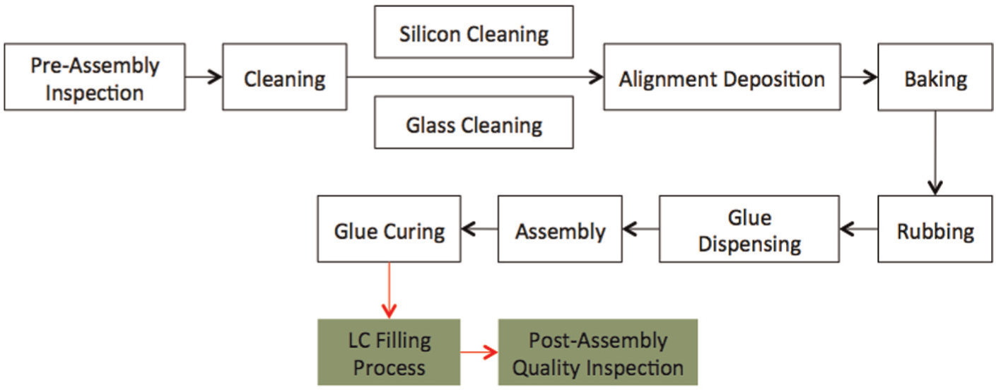
Designed assembly process for phase-only liquid crystal on silicon devices.
In this research, some further development of the die-level assembly process for phase-only LCOS devices is presented, particularly the techniques for LC filling and overall device quality assessment. The details of the LC filling process using an in-house designed equipment with a temperature-adjustable system are described. In addition, an optical microscope is employed to inspect the assembled LC layer and measure its thickness. As a result, the assembled phase-only LCOS devices show in the post-assembly inspection the required thickness tolerances for the LC layer (<λ/4) and a high reproducibility. These devices support our own research such as free space 20 and fibre switches,21,22 optical interconnects in crosstalk mitigation as well as other research institutions and industrial users for their system development and product evaluation.
LC filling process
LCOS devices should be filled before mounting and bonding in order to avoid uncertain contamination to ingredients of LC materials. The alignment quality should also be assessed before filling process. 23 For example, the rubbing cloth might be left on the substrates during the rubbing process. Contamination from the sealing glue lead to two major effects: one is the creation of secondary electric layers that decrease the effective voltage across the LC layer; the other is the weakening of the alignment strength by bonding to the surface of the alignment material.
The filling hole with a premeditated size should be left so that the LCs can be efficiently filled without any blockage. In general, for non-linear LC materials, three major aspects of material parameters should be considered: the birefringence, viscosity and temperature requirement for the phase transition from the nematic to the isotropic. In practice, on one hand, heating might help for the filling process; however, composition of LC materials might be changed during the heating process and this leads to the reduction in the optical properties of LC materials such as birefringence and dielectric anisotropy.24–26 On the other hand, if the isotropic phase temperature of the LC is not reached during the filling process, there is a possibility that the nematic filling flow will affect the alignment of the LC so that the molecules do not lie in the rubbed grooves. This will affect the LC off-state alignment and degrade the switching performance of the LCOS device ultimately. Therefore, an optimised heating process to the nematic phase is required with a high degree of experience. The steps change when different LC materials are applied. In practice, phase-only LCOS devices are filled with the LCs in the isotropic phase as fast as possible without changing the composition of LC materials.
The filling process uses in-house designed vacuum filling rig as shown in Figure 2. This filling rig consists of two heating stages (red), the LC container (blue), joystick (green) and pumping system (grey). The joystick is used to dip the needle into the LC material and feed the device at the filling hole. It allows the device and the LC to be heated separately. An appropriate heating of the LC material will speed up the outgassing process so that gas bubbles in the material can be released more efficiently. This can help to avoid gas bubbles being created in the filled devices and the desired optical performance can be guaranteed.
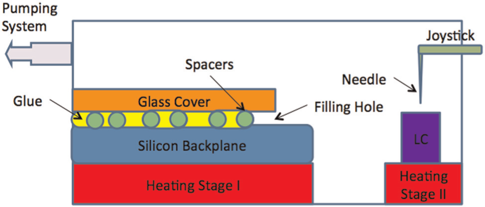
Cross-sectional schematic of the designed LC filling rig.
Inspection of the filled LCOS device reveals any problem in the assembly process, such as scratches on the substrates, filling flow effects and glue deposition quality. It is an essential step in the quality control of the LCOS device, offering feedback that will allow improvement of the assembly technique.
In Figure 3, pictures are taken by the BX51 microscope through crossed polarisers in the dark state. Figure 3(a) and (b) shows a comparison between an empty and filled LC device. As can be seen in the empty device, the glue line is deposited uniformly and does not come into contact with pixel array. Note: the visible stains are on the front surface of the glass outside the device. However, inspection of the filled devices reveals alignment defects caused by microscopic damage to the alignment layer during handling. For example, the scratches observed at the left upper corner on the glass substrate. The LC filling process spreading corrugations from the filling hole can also be inspected. These corrugations are caused because the environmental temperature does not reach the clearing point (isotropic phase) during the filling process (so-called flow alignment). Furthermore, corrugations may occur if the speed of LC material filling is too fast, due to either an abrupt release of the air pressure in the vacuum chamber or an oversized filling hole because of poor control of the glue dispensing. In brief, LC filling is a critical process step which requires accurate temperature control and suitable gas releasing. Also, it needs to be completed as quickly as possible in order to avoid changing the composition of the LC. Figure 3(c) shows an example of an LCOS device filled with LC in isotropic phase; thus, no flow alignment occurs and the planar alignment with 2° pre-tilt angle is obtained using the rubbing machine AZ-LCD MF7.
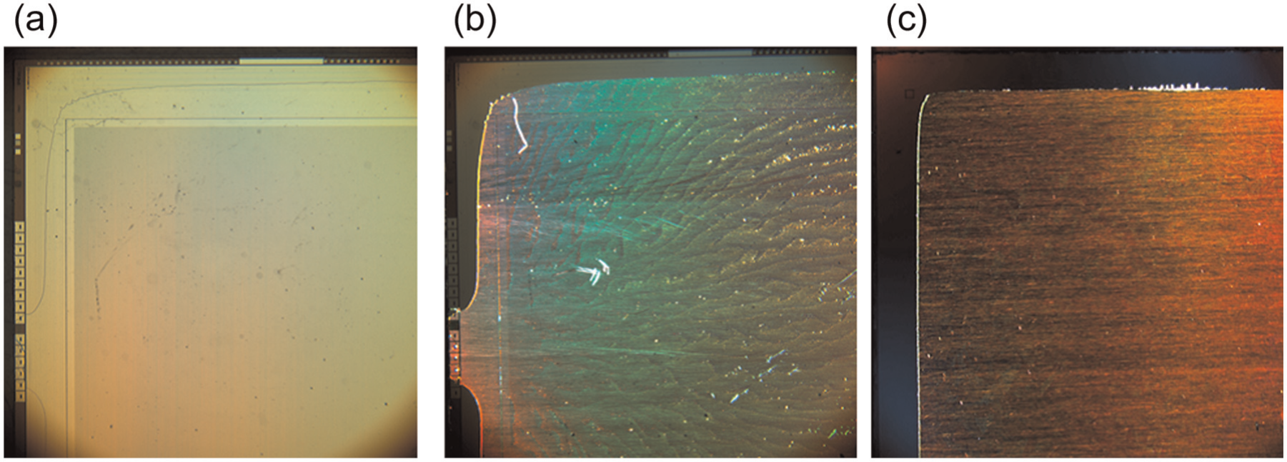
Comparison of LC filling process at the same area of a phase-only LCOS device between the (a) empty and (b) filled states; (c) the typical example for the LC filling process in isotropic phase.
Overall quality assessment
A die-level assembly process for assembling pre-production prototype phase-only LCOS devices of high quality has been developed using a semi-automated program-controlled robotic tool (SET Technology Kadett). The overall assembly assessment can be summarised in three major parts which are device thickness uniformity, glue line robustness and in-cell characteristics including LC filling process, alignment rubbing and so on. Figure 4 shows an example of the desired quality of devices to illustrate the overall quality of assembled device. In Figure 4, the interferogram is taken using mercury light (365–436 nm) and Xenon arc light. The image was captured between cross-polarisers, including differential interference contrast (DIC) prism and objective. These two images normally indicate a number of characteristics of assembled cell. Firstly, the uniformity of the LC layer thickness can be evaluated by observing the colour variation across the pixelated area using an optical microscope through cross-polarisers. For instance, the red colour is observed in most of the areas and the rest is mainly green as shown in Figure 4(a). This shows that the cell is likely to achieve the desired quality for thickness uniformity and it is worthwhile to proceed to the next step of the detailed thickness measurement as shown in Figure 4(b). Secondly, the glue dispensing characteristics shown in Figure 4(a) are also inspected. The width of the deposited glue line should be controlled wide enough (about 1.5–2 mm) to seal the device firmly but without approaching the pixel area depending on the layout of the VLSI circuitry (20 mm × 15 mm). In addition, the size of the LC filling hole should be 1–3 mm depending on the layout of pixelated array in order to maintain the device uniformity and guarantee an efficient material filling process. Thirdly, the alignment layer is formed by rubbing the deposited polymide in order to avoid reverse tilt. The effect of LC alignment can be seen as the color difference at the boundary of the applied voltage in Figure 5. Because of the colour uniformity shown in Figure 5, it indicates that LC filling process has been executed in isotropic phase. The thickness contour in Figure 4(b) is employed for thickness measurement. The details of thickness measurement are shown in Table 1, where ‘N’ denotes the device has been divided into 15 areas (3 × 5); the measurement for each area is calculated and then the mean value and standard deviation are obtained.
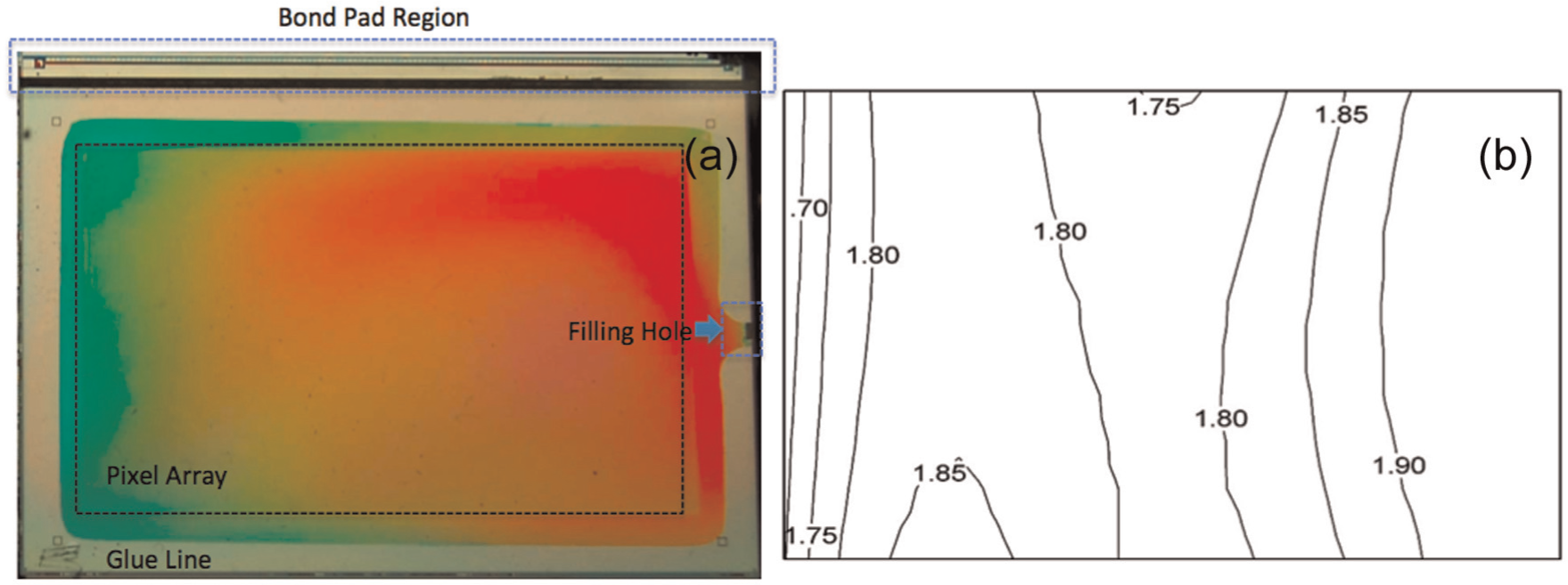
(a) Interferogram and (b) the thickness measurement of a high-quality phase-only LCOS device using an Olympus BX51 microscope. Note: the interferogram is taken by the BX51 microscope through crossed polarisers; the method of thickness measurement is summarised in a separate section at the end of this article.
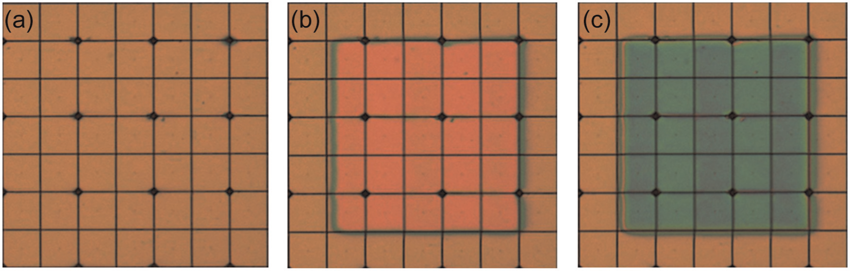
An enlarged view of a 5 × 5 pixel array displayed with different voltages through cross-polarisers using BX51 microscope: (a) without any applied voltages, (b) 1.4 V is applied across the device and (c) 1.6 V is applied to the same area. The pixel pitch is 15 µm.
Statistics of thickness for the device (Figure 4).
Average LCOS thickness is 1.816 µm; the standard deviation is 90 nm.
Conclusion
An established LC filling process and statistical overall quality analysis have been developed for die-level assembly process to ensure the excellent quality of pre-production prototype phase-only LCOS devices. A designed rig is able to implement the LC filling process with moderate filling speed and appropriate filling temperature so that the LC composites can be maintained and injected to the cell without producing the damage to the alignment layer during the filling process. It indicates that ‘proof-of-principle’ phase-only LCOS devices are successfully assembled with the flexibility in choosing the right LC materials and different silicon backplanes. More importantly, the quality of the assembled devices is comparable to that from a commercial high-volume production line. To summarise, the die-level assembly quality for phase-only LCOS devices can be produced with a number of distinguished features: (1) excellent spatial uniformity (less than of λ/4 ≈ 150 nm), (2) robust glue sealing process and effective UV exposure to maintain the seal strength, (3) LC materials uniformly aligned with no ‘flow alignment’ effect, and (4) quality assurance of individual devices by inspections at each assembly stages.
Method
Robotic tools are from SET called K1 Kadett, and the die-level assembly process has been performed in class 100 and class 1000 clean room. Thickness measurement using an optical microscope is introduced.
The cell thickness of an empty device was measured using an interference method. When the cells are illuminated, some of the incident light is reflected directly, and some is transmitted and reflected from the back of the glass plate. There is a phase difference δ between rays of wavelength λ given by
where n is the refractive index, and d is the cell thickness. It is assumed that the intensity of further reflections is negligible. At certain wavelengths, a phase difference of some odd multiple of π occurs, causing the two sets of rays to interfere destructively and result in minimum transmission. For two consecutive wavelengths that satisfy this condition in air (n = 1.00)
This suggests that plotting successive values of 1/λ min against integer steps will give a straight line with slope of 1/2 d. In the cell thickness calculation, the minima were found using MATLAB. Local minima were found based on their first and second derivatives, and more accurate values were obtained for the minima by approximating each ‘valley’ as a parabola. This was necessary because some of the minima were asymmetric or noisy. The thicknesses were evaluated using a least squares regression. As an example, the transmission spectra for one of the cells both empty and filled are shown in Figure 6. A correlation coefficient of 0.9999 or better for each linear regression performed on data from each cell confirms the above equation.
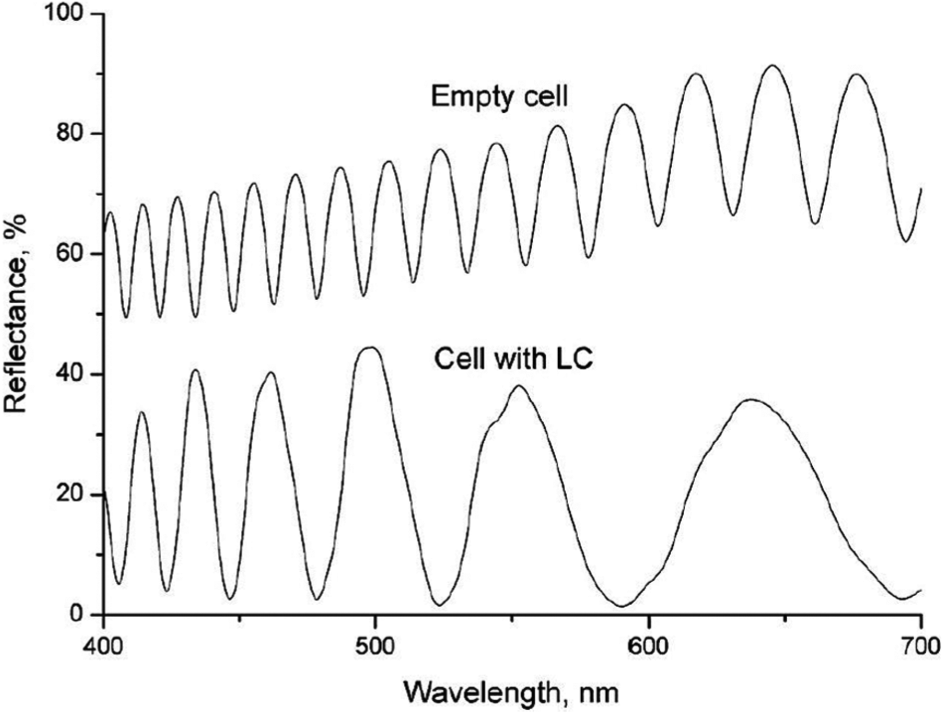
Reflection spectra for an empty device and a device filled with LC between crossed polarisers.
The spectra of a cell filled with LC show clear points of minima at near-zero intensity corresponding to phase shifts of 2π. The wavelengths λm at which these occurred were used to calculate the phase shift across the spectrum by interpolation.
Footnotes
Declaration of conflicting interests
The authors declare that there is no conflict of interest.
Funding
This work was supported by State Key Laboratory of Precision Measurement Technology and Instruments, Tsinghua University. It was also supported by National Natural Science Foundation of China (61307077), Beijing Natural Science Foundation (4144076), China Postdoctoral Science Foundation (2013M530613), the UK Engineering and Physical Sciences Research Council (EPSRC) through the Platform Grant in liquid crystal photonics (EP/F00897X/1) and the Cambridge Integrated Knowledge Centre (CIKC) through projects PASSBACK and PASSBACK3.