
Abstract
A newly developed sol-gel (SG) polishing pad can satisfy the processing demands of SiC wafers by providing scratch-free polished surfaces with nano-roughness. The main characteristic of this polishing tool is the semi-fixed abrasive together with the flexible matrix. In this article, contrastive experiments involving polishing of SiC wafers with three different types of tools were conducted to confirm the machining mechanism of the SG polishing pad. The results indicate that the abrasives in the pad exhibit yielding effects during the polishing process, contributing to the achievement of a mirror-like wafer surface. In addition, larger abrasives can be chosen for the SG polishing pad to obtain relatively high wafer surface quality instead of smaller ones, thereby avoiding the agglomeration problem of ultrafine abrasives.
Introduction
Polishing is a process of removing excessive topographic variations and achieving global and local planarisation. 1 As a crucial procedure of finish machining, the precision of polishing determines the value of the other preceding mechanical processes, especially in the microelectronic device fabrication industry, which requires a mirror-like surface with extremely high integrity.2–5 Common polishing methods can be divided into free abrasive polishing and fixed abrasive polishing according to the fixation state of abrasives. Free abrasive polishing has been considered as the main method of precision and ultra-precision machining because it can obtain micro- or even nano-scale smooth surfaces.6–8 Chemical mechanical polishing (CMP), as a typical method of free abrasive polishing, is widely and effectively used and has been regarded as a key technology to achieve high-quality surfaces by reducing roughness and removing damaged layers.9–11 However, CMP is prone to form agglomerated particles, resulting in pits on the wafer surface because free abrasives are uncontrollable during polishing. From the tribological perspective, free abrasive polishing belongs to a three-body wear mechanism, in which abrasive particles are free to roll and slide between two surfaces and cause wear on at least one of the two surfaces.12,13 Compared to free abrasive polishing, abrasives are inlayed in the matrix in the fixed abrasive polishing to confirm that each particle has its own position. However, it is difficult to get the abrasives uniformly distributed in the tools, especially when ultrafine particles are aggregated together. Moreover, the lack of uniformity is prone to cause mechanical damages due to the uneven exposed heights and the hard matrix.14–16
To minimise the problems existing in free and fixed abrasive polishing, many approaches have been attempted to create non-traditional polishing tools. Semi-fixed abrasive polishing is a promising breakthrough. Yuan et al. 17 proposed semi-fixed machining tools with a ‘trap in effect’, for which surface damage induced by the larger abrasive particles can be reduced or even eliminated. Shih et al. 18 embedded diamonds in a polishing pad mixed with a surfactant, a polymer and a curing agent. Nakamura et al. 19 introduced a new gel granulation method to fabricate SiO2, Al2O3 and Cr2O3 polishing discs. Liu et al.20,21 and Hu et al.22,23 created sol–gel polishing pad with alumina and diamond abrasives, respectively. In this article, a SG polishing pad, a flexible semi-fixed polishing tool with diamond abrasives uniformly distributed utilising sol–gel technology, is introduced. The difference between the SG polishing pad and other polishing tools is the flexible matrix made of sodium alginate (AGS). Contrastive experiments involving fixed abrasive polishing, semi-fixed abrasive polishing and free abrasive polishing are conducted to investigate the machining mechanism of polishing of SiC wafers using SG polishing pads. The surface roughness (Ra), surface morphology and material removal rate (MRR) of each of the polished wafers together with the wear of the tools are analysed.
Experimental
Fabrication process of the SG polishing pads
AGS are linear chains of (1,4)-linked monomers of b-
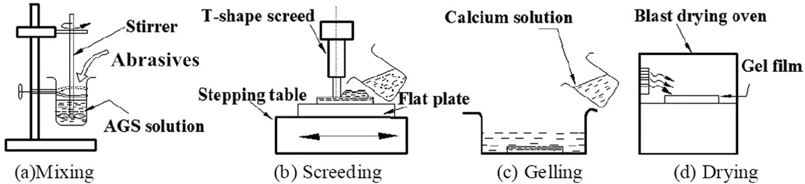
Schematics of the fabrication process of the SG polishing pads.
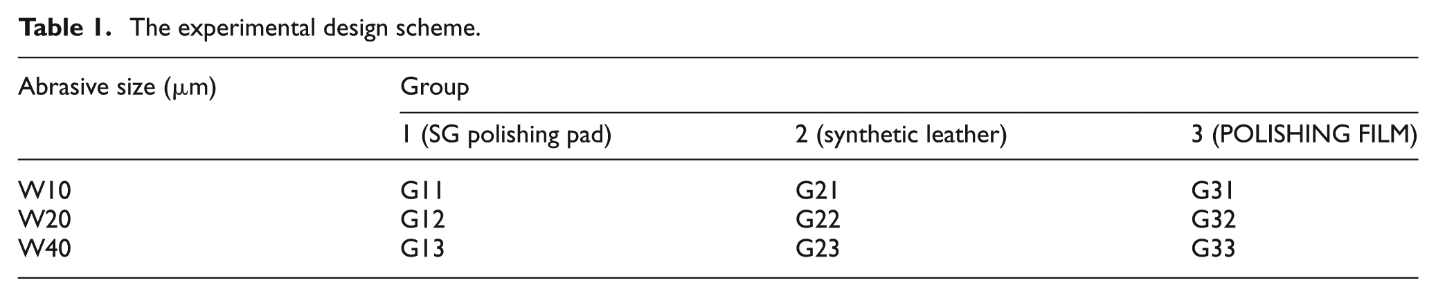
Experimental design
The experimental design involves three groups of tools. The polishing tools used in group 1, group 2 and group 3 were SG polishing pad, synthetic leather pad with free abrasives and POLISHING FILM, respectively, representing three different types of polishing, that is, semi-fixed abrasive, free abrasive and fixed abrasive. Each group contained three types of diamond abrasives with different particle sizes. All of the experiments were performed under the same conditions to exclude the influence of external factors. In group 2, the synthetic leather pad was used to hold the slurry with 1 wt% diamond abrasives. The POLISHING FILM used in group 3 is an industrial polishing pad manufactured by electrostatic absorption. The SiC wafers with surface roughness varying from 80 to 90 nm had a diameter of 2 in and a thickness of 400 µm. The surface morphologies of the SiC wafers and the polishing tools were observed using a Hirox KH-8700 optical microscope attached to a digital video system. The surface roughness (Ra) was measured using a ZYGO three-dimensional (3D) optical surface profiler. A total of 10 different areas were measured to reflect the overall situation of the polished surface. Meanwhile, a Sartorius balance was used to weigh the mass loss of the polished wafers. The weighting was repeated three times and the mean value was calculated for the sake of decreasing the errors due to the measurements being performed manually. Surface morphologies together with the values of Ra and MRR were detected every 20 min to reveal the whole polishing process in detail. The experiment design scheme is presented in Table 1.
The experimental design scheme.
All of the experiments were performed on a UNIPOL-1000s auto press polishing machine, as shown in Figure 2(a). The SiC wafers were stuck on the sample holder by paraffin. The polishing tools were pasted on the lapping plate by the double-faced adhesive tape. The sample holder and lapping plate rotated in the opposite direction drove by the electromotor, as shown in Figure 2(b). The difference between the three groups was the slurry feeding system. In groups 1 and 3, the circulating pump was used to provide circulatory deionised water. An automatic slurry feeder, such as the one shown in Figure 2(c), was selected because free abrasives were required in group 2. Free abrasives could not only alleviate the aggregation of diamond abrasives to a certain degree by stirring the slurry uniformly but also steadily provide the slurry. The rotation speed ratio of the lapping plate and sample holder was set as 1.1 according to the abrasive path simulation. All of the polishing parameters were set to ensure the relative appropriate condition for the three types of polishing. The experimental parameters are presented in Table 2.
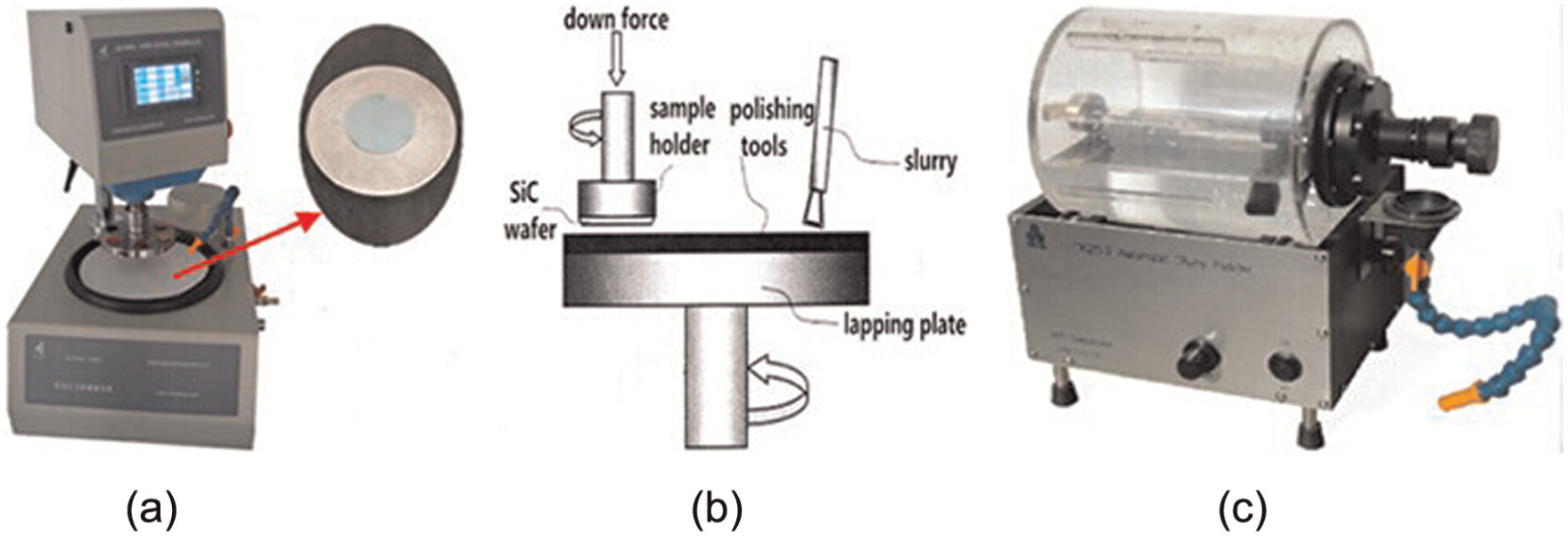
Experimental facilities and conditions: (a) polishing machine, (b) illustration of experiment and (c) automatic slurry feeder.
The experimental parameters.
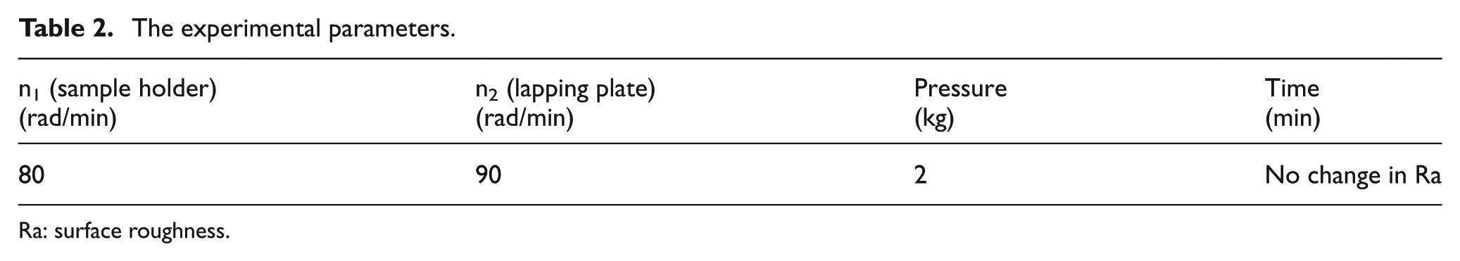
Ra: surface roughness.
Results and discussion
Abrasives with the same size: working nearly in the same horizontal line
Figure 3 shows the mean value and variance of Ra obtained on the surfaces polished by three polishing tools with 20 µm abrasives. The surfaces of the original wafers are uneven, with variance of Ra more than 10. The variance decreases as the polishing process proceeds. The surface polished by the SG polishing pad has the most distinct range of decrease, with the variance changing from 11 to 0.1 (shown in Figure 3(a)), while the other two groups exhibit decreases of 11 to 1 (shown in Figure 3(b)) and 11 to 0.9, respectively (shown in Figure 3(c)). The ultimate variance of G12 only takes 20% of G22 and 10% of G32. Moreover, the variances of G12 are far below the other two during the entire process. The result indicates that the surface polished by the SG polishing pad is extremely uniform. Surface morphologies can reveal the difference of surface homogeneity directly. Compared to the pits and scratches appearing for the other two methods, hardly any defects are found on the surface polished by the SG polishing pad.
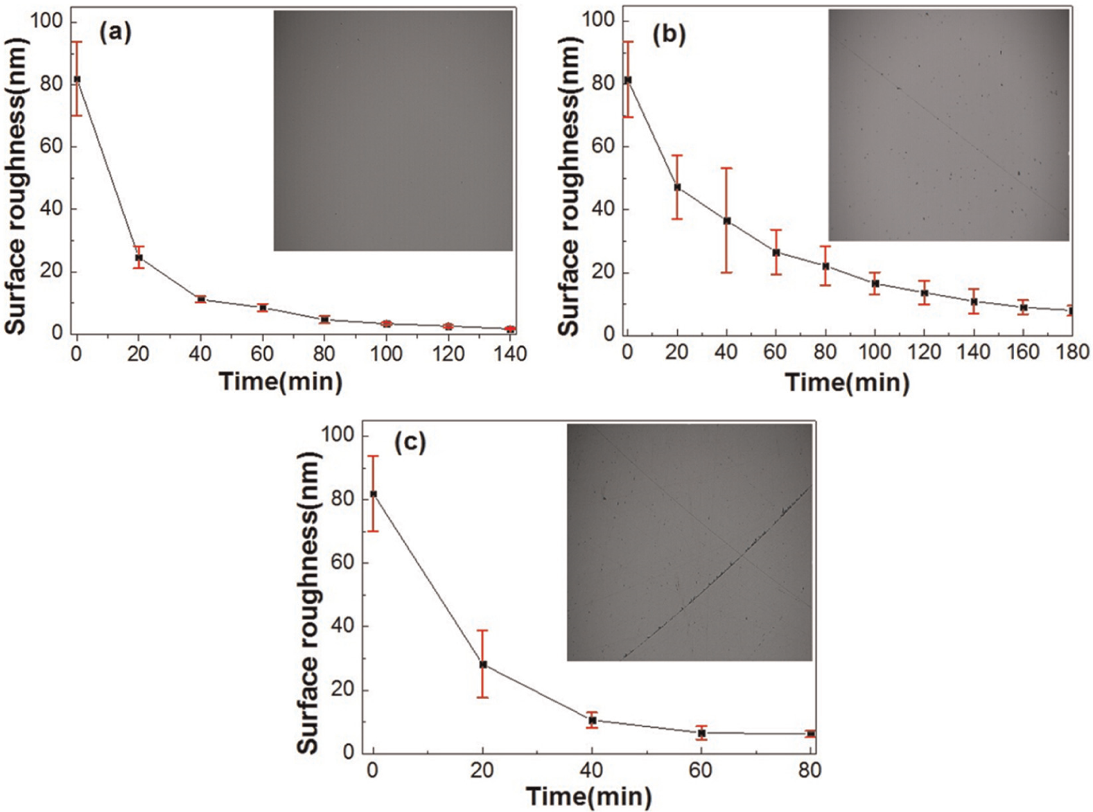
The mean value and variance of Ra obtained on the surfaces polished by (a) W20 SG polishing pad (G12), (b) W20 free abrasive polishing (G22) and (c) W20 POLISHING FILM (G32). The inset shows the corresponding surface morphologies (1000×).
The surface profile reveals the grinding effect of abrasives on the wafers: the top is produced by the scratch stagger of different abrasives, and the bottom represents the grinding depth. Therefore, the surface profile could reflect the state of the working abrasives. As shown in Figure 4(a), the gaps between the bottom and its nearest top are almost the same, approximately 1.7 nm. Taking into consideration the surface profile of the SiC wafer polished by the W20 POLISHING FILM, just as that shown in Figure 4(c), the gaps are extremely uneven, varying from 3 to 15 nm, which suggests the abrasives with different exposing heights grind the surface at the same time. The synthetic leather pad is relatively soft and can provide a flexible matrix that is similar to that of the SG polishing pad; thus, the gaps are approximately several nanometres, as shown in Figure 4(b).
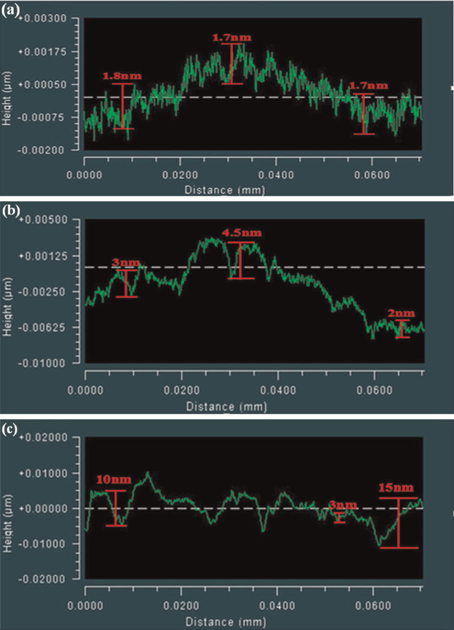
Surface profile of SiC wafers polished after 80 min by (a) W20 SG polishing pad, (b) W20, free abrasive polishing and (c) W20 POLISHING FILM.
The morphologies of the polishing tools at different times are presented in Figure 5. As shown in Figure 5(a), white circles emerged around the abrasives after 20 min of polishing, which indicated that the abrasives would swing under a certain pressure. With further progress of the polishing process, the grinding height of the abrasives became smaller because the wear became increasingly serious. As a result, the matrix comes into contact with the wafer surface to a certain extent, leading to the generation of the flow patterns. This manifestation of this phenomenon was extremely distinct after polishing for 80 min. However, no broken abrasive was found, although some abrasives fell off from the flexible matrix. Compared to the variation of the SG polishing pad, removed SiC dust emerged on the matrix of the POLISHING FILM (Figure 5(b)) after polishing for 20 min. The broken abrasives started to emerge and became worse as the polishing progressed.
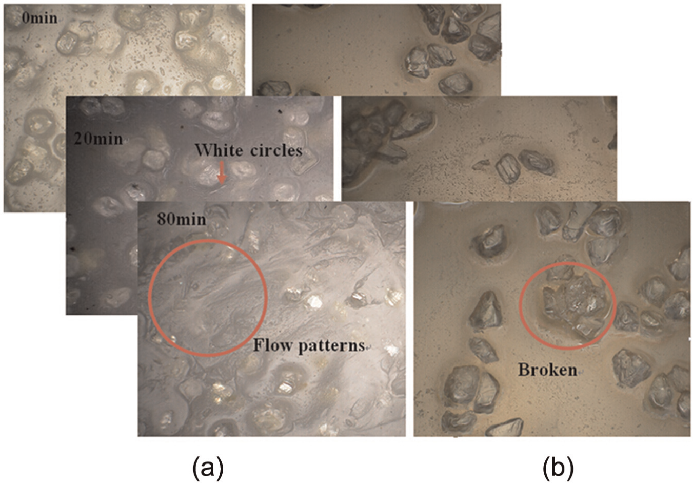
Morphologies (350×) of the polishing tools at different times: (a) W20 SG polishing pad and (b) W20 POLISHING FILM.
For the SG polishing pad, the pinnacle abrasives will yield to the flexible matrix partly when they come into contact with the wafer surface. The higher the abrasive particle is, the more it yields to the flexible matrix. Abrasives with different exposed heights can work nearly in the same horizon line, as shown in Figure 6(a). The white circles are the result of abrasive yielding in the flexible matrix. When grinding force of abrasive is so high that the flexible matrix cannot provide sufficient bonding force, the abrasive particles will fall off, thus avoiding the formation of scratches on the wafer surface. In the common polishing process, the locations of the abrasives are basically fixed due to the hard matrix. As shown in Figure 6(b), for the abrasives at higher positions that come into contact with the wafer, scratches form under the motion of these higher abrasives that ‘trap’ them into the wafer. Subsequently, scratches with different depths intersect with one another. Abrasives are more likely to break down if the grinding depth changes sharply or the wear becomes more serious.
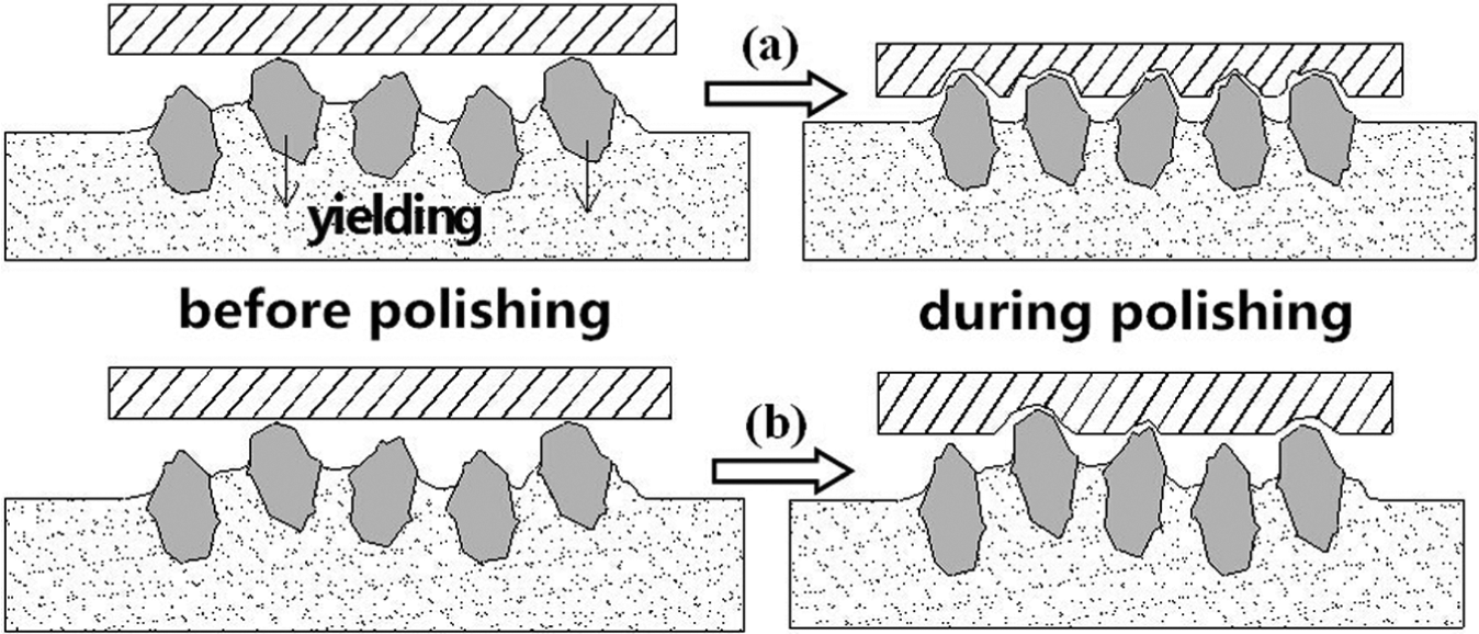
The state of the abrasives before and during the polishing process: (a) SG polishing pad and (b) common polishing tools.
Abrasives with different sizes: exhibiting exposed heights with little difference
Figure 7 presents the MRR of SiC wafers after polishing for 80 min. The MRRs of the wafers polished by the SG polishing pad are much smaller than those of the others under the same conditions. A smaller MRR signifies that the polishing pad is less prone to produce surface and subsurface defects. The 3D white light interferometric micrographs of the polished wafers shown in Figure 8 indicate that many pits are produced on the surface machined by free abrasive polishing and that deep scratches instead of pits are found on the surface polished by the POLISHING FILM. In contrast, hardly any defects are found on the surface polished by the SG polishing pad.
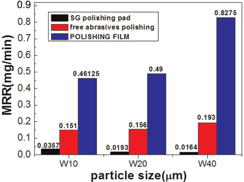
MRR of the SiC wafers after polishing for 80 min.
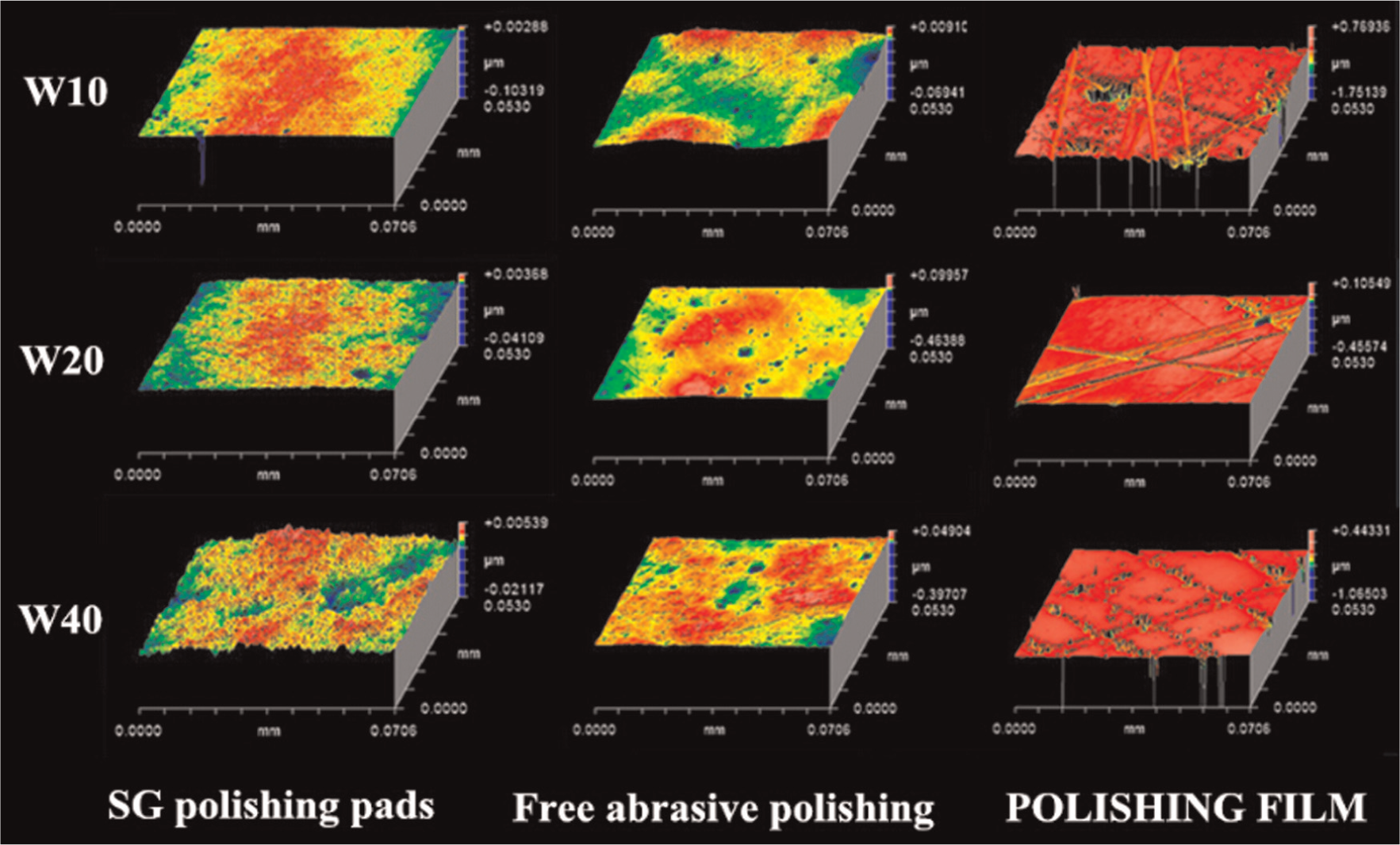
Three-dimensional white light interferometric micrographs of the polished wafers.
The changing trends of Ra obtained on the surfaces polished by the three different tools are presented in Figure 9. As shown in Figure 9(a), the machining effects of the SG polishing pad with different abrasive sizes are quite similar. In the case of polishing for 80 min, when the abrasive size varies from initially 10 µm up to 20 and 40 µm, the increases in the range of Ra are 3.41 and 1.89 nm, respectively. The results of the POLISHING FILM shown in Figure 9(c) indicate that the increased range of Ra is 5.51 and 20.95 nm for the abrasive sizes of 20 and 40 µm, respectively, which are much higher than the case of the SG polishing pad. This phenomenon exists throughout the entire polishing process. Figure 9(b) shows the changing trend of Ra measured on the surface polished by free abrasive polishing. Because the soft synthetic leather provides a matrix similar to that of the SG polishing pad, the polishing effect is similar to that of the SG polishing pad.
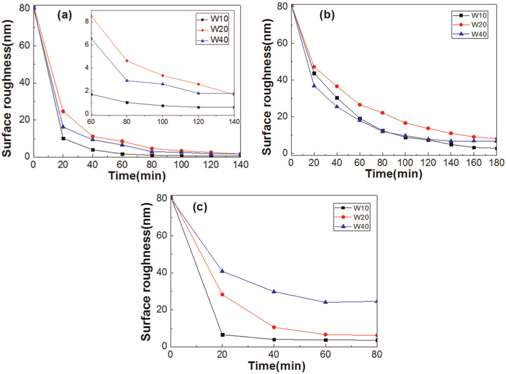
The trend of Ra obtained on the wafer surfaces polished by (a) SG polishing pad, (b) free abrasive polishing and (c) POLISHING FILM.
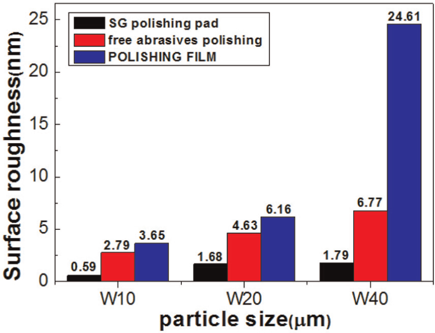
The ultimate Ra obtained on the wafer surfaces is shown in Figure 10. The values of Ra of the surfaces polished by the SG polishing pad are far less than those polished by the other two tools using the same abrasives. The phenomenon is most obviously manifested in the situation of W40 abrasives. The ultimate Ra obtained on the surface polished by the W40 SG polishing pad is 1.79 nm, while the values are 6.77 and 24.61 nm for the free abrasive polishing and the POLISHING FILM, respectively. Ra of 1.79 nm is even much lower than the values of 2.79 nm (Ra obtained in G21) and 3.65 nm (Ra obtained in G31). Taking into consideration the changing trend of Ra in Figure 9, the SG polishing pad is found to provide better surface precision using larger abrasives instead of the smaller ones.
Ultimate Ra obtained on SiC wafer surface.
The abrasives will yield to the flexible matrix during the polishing process. Within a certain range, the larger the abrasives are, the deeper they yield to the flexible matrix. The effects of abrasive yielding in the polishing process reduce the size differences of the abrasives, enabling the abrasives to have a relatively smaller grinding height. As a result, higher surface precision can be obtained using the SG polishing pad with larger abrasives. When the abrasives are so small that they have a particle size on the order of micro- to nanometre, it is difficult to avoid the agglomeration of the ultrafine abrasive powders, which will reduce the processing precision to a large extent.
Conclusion
The machining mechanism of the SG polishing pad on silicon carbide wafers was clarified through experiments comparing three different types of polishing methods. Scratch-free wafer surfaces with nano-roughness can be obtained after being polished using the SG polishing pad. The flexible matrix made of AGS in the SG polishing pad allows abrasives to yield when they come into contact with the wafers. The effect of abrasive yielding in the polishing process leads to the results below.
First, abrasives with different exposed heights can grind the work-piece uniformly, almost on the same horizon line; thus, no scratches or pits are produced.
Second, within limits, abrasives with different sizes have almost identical exposed and grinding heights. Finer abrasives, which are typically used to obtain higher machining precision, can be replaced by more coarse ones, resolving the agglomeration problem of the ultrafine abrasive powders in the tools.
Footnotes
Declaration of conflicting interests
The authors declare that there is no conflict of interest.
Funding
The authors appreciate the support from the National Natural Science Foundation of China (Grant No. U1034006, 51105149), the Specialised Research Fund for the Doctoral Program of Higher Education (Grant No. 20133501130001) and the Fujian Education Department (No. JA13006).