
Abstract
The light trapping surface of micro–nanostructure can significantly improve the performance of optical transmission and can greatly reduce the broadband domain of material surface reflectivity, which means the material surface absorptivity on wide-spectrum signal is enhanced. Several commonly used methods for manufacturing micro–nano surface of light trapping structure with low reflectivity are introduced first, including chemical etching, mechanical grooving, reactive ion etching, common long-pulse laser grooving, and ultra-fast pulse laser processing. This is followed by a comparison of the advantages and disadvantages of these methods. Among these methods, ultra-fast pulse laser processing is an ideal manufacturing technology for fabrication of light trapping structures. The research status of the micro–nano manufacturing technology of structured surfaces for light trapping with low reflectivity is reviewed, and emphasis is given to their application prospects. The research directions and trends of the micro–nano manufacturing technology of structured surfaces for light trapping with low reflectivity are summarized, and broad application prospects and research value in many fields, such as solar cells, solar water heater, building wave-absorbing materials, information acquisition of mechanized equipments, high-radiation heat exchange equipment, solar heating equipment, and solar air conditioner, are pointed out.
Keywords
Introduction
There is an ever-growing worldwide energy demand, which has also resulted in a recent global energy shortage. Traditional fuels used in the production of energy such as fossil fuels have raised various environmental concerns. As a result, research and development along with the utilization of renewable energy sources are being given priority and sources such as solar energy are becoming increasingly important.1–3 In addition, there is an impetus toward the development of various appliances such as solar cells, solar water heater, solar heating equipment, and solar air conditioner. The development and utilization of solar energy are closely tied to the research on development of low surface reflectivity of materials and their utilization to enhance energy efficiency. Meanwhile, with the rapid progress and development over the recent years in various technology fields such as acoustics, optics along with electrical engineering has greatly enriched the means of information acquisition. Information acquisition refers to techniques related to the measurement, storage, perception, and collection of information from a variety of sources. 4 Among these techniques, the important information technology and of particular interest here is direct acquisition. 4 Currently, the main information acquisition techniques are sensor technology, telemetry, and remote sensing technology. 4 Information acquisition techniques that use low reflective material surfaces would allow the use of surfaces on buildings and mechanized equipment, allowing electromagnetic waves to be easily absorbed and reduction of signal reflection. Low reflective material surfaces on buildings would isolate and continuously reduce aggravated electromagnetic pollution. Whereas low reflective material surfaces on mechanized equipment would allow implementation of effective information acquisition by allowing capture of electromagnetic waves to gain information, as well as preventing information loss.
At present, there are many methods that can be used to reduce the material surface reflectance, the most widely and commonly used method is in which a material with lower reflectivity is directly applied or coated onto the surface of the material.5–9 Such a special material treatment method mainly focuses on the research and development of lower reflectivity materials and belongs to the category of material treatment. However, because of different thermal expansion coefficients of different materials and instability after heating, the special material treatment of surfaces with low reflectivity often fails. It is also very important that the method for reducing reflectance can accommodate the surface shape of material with special structure without directly changing the physical structure or morphology of material surface to increase the material’s surface roughness.10–13 This reduces the reflectance of material surface to achieve high absorption of the signals. Such a processing method belongs to the category of material surface–structured processing and has the advantage of long service life.
The studies found that micro–nanostructured material surfaces with unique optical properties result in new phenomena; they especially greatly reduce broadband domain reflectivity of the material surfaces and enhance the absorptivity of wide-spectrum signal on the material surface.14–17 In order to improve the solar energy utilization efficiency of solar cells, solar water heater, solar heating equipment, and solar air conditioner along with reduction of electromagnetic pollution from buildings and mechanized equipments with the goal to improve environmental protection consciousness and effects of information acquisition, we present micro–nanostructured material surface processing using advanced micro–nano manufacturing technology to increase the material’s surface roughness and reduce reflectivity of the material surface. It is necessary to increase the effective absorption of wide-spectrum light wave signal, and it has important practical significance. Based on this, several commonly used methods in the micro–nano manufacturing of structured surfaces for light trapping with low reflectivity are introduced in this article, and their advantages and disadvantages are analyzed. The research status of the micro–nano manufacturing technology for light trapping structure with low reflectivity of material surface in China and abroad is also summarized, and application prospects are discussed.
Micro–nanostructure manufacturing methods with low reflectivity of material surface
Micro–nanostructure manufacturing for low-reflectivity material surfaces commonly uses methods such as chemical etching,18–21 mechanical grooving,22,23 reactive ion etching (RIE),24–26 common long-pulse laser grooving,27,28 and ultra-fast pulse laser processing.29–31 Among these methods, chemical etching method and mechanical grooving method are the most widely used and the most mature technologies. In addition, common long-pulse laser grooving technology is another method that is also frequently used. The benefits and limitations of commonly used manufacturing methods for micro–nanostructure surfaces with low reflectivity are shown in Table 1.
The benefits and limitations of commonly used manufacturing methods for micro–nanostructure surface of low reflectivity.
RIE: reactive ion etching.
Chemical etching methods18–21 use chemical etchants such as dilute sodium hydroxide solution, aqueous solution of hydroquinone phosphate, and aqueous solution of ethanolamine to etch the surface of the materials and form a rough surface. Chemical etching methods can be broadly classified into two categories based on the etch directionality as anisotropic etching and isotropic etching. For civilian applications of silicon-based materials commonly used in solar cells, anisotropic etching methods are suitable for surface treatment of monocrystalline silicon to prepare the light trapping structure. The light trapping structure is formed by 2–10 µm uniform-sized pyramid-like structures on the surface of monocrystalline silicon. This structure can improve the efficiency of the monocrystalline silicon solar cells from 9.9% to over 15%.32,33 However, it is not suitable for surface treatment of multicrystalline silicon, which is due to the random distribution of the crystallographic orientation for the crystal grains of multicrystalline silicon. As a result, it cannot form the uniform surfaces of the pyramid, and at different inter-granular boundaries, a difference in the corrosion rate will cause a large number of stairs and affect the subsequent production of the solar cells. The caustic etchant used for isotropic etching is generally an acid solution with the same corrosion rate in each crystallographic orientation for the crystal grains of silicon, which is suitable for fabricating the light trapping structure and the surface treatment of multicrystalline silicon and would improve the light absorption performance to a certain extent.34,35 In Tsujino et al., 34 multicrystalline p-type silicon wafers were textured in hydrogen fluoride (HF) solution by chemical etching, and the solar cell device manufactured from these textured silicon wafers showed significantly reduced surface reflectance with efficiency as high as 16.6%. Ju et al. 35 used an acidic solution of HF:HNO3:CH3COOH:deionized (DI) water (8:21:10:8 ratio) and the vapor-textured HF:HNO3 (7:3 ratio) with 8 g of silicon on the multicrystalline p-type silicon wafers to achieve an etching depth of about 4 µm in 3 min after etching on both sides of mc-Si wafers and a nanoscale porous surface with pore size less than 50 nm after 8.5 min. For these surfaces, the average reflectance was 22.16% and 6.5%, and the efficiency of solar cells was about 15.43% and 15.98%, respectively. However, chemical etching methods require a large volume of chemical solutions, which result in serious environmental pollution and are hazardous to human health. Also, for the formation of light trapping structure, chemical etchants offer poor control to regulate the shape thereby limiting the light absorption rate.
Mechanical grooving technology22,23 is mostly surface grooving with multiple blade grinding wheel to form a V-textured structure. This method has the advantages of being a simple, low cost, with higher processing efficiency, precisely controlled structure shape and arrangement, but it is limited by the grinding wheel processing precision. Mechanical grooving technology can be used to produce microstructures with a minimum depth of 50 µm. Therefore, it requires material thickness that is above 200 µm to reduce the effect of mechanical stress and damage resulting from the mechanical grooving process, which easily forms the defects that influence the utilization performance. In Spiegel et al., 22 solar cells with mechanically V-textured multicrystalline silicon on low-reflectivity surfaces obtained efficiencies as high as 16%−16.3%, which show 4%−7% relative improvement in efficiency when compared to untextured reference cells.
RIE24–26 can be used to fabricate light trapping structures with high precision at the micro- or nanoscales by etching material using plasma etching, but it requires a relatively complex process and an expensive processing system which can cause mechanical stress and damage. Light trapping surface texturing processed by RIE techniques can reduce reflection and improve efficiencies of solar cells. This method can obtain the pyramids of needle-like structure with diameters ranging from 50 to 70 nm on the surface of silicon, which the minimum reflectance of wavelength ranging from 400 to 1200 nm reaches about 5.6%.24–26
Conventional common long-pulse laser grooving technology27,28 is used to fabricate light trapping structures on material surfaces by common long-pulse laser ablation processing method; its advantage lies in the fabrication of different grooving styles, such as striped and inverted pyramid shape and the flexibility to adjust the shape characteristics of the light trapping structure. These advantages contribute to the improvement and optimization of the light trapping structure. However, conventional common long-pulse laser grooving technology similar to the mechanical grooving technology can process larger scale microstructures to restrict the material thickness and increase the cost. At the same time, the surrounding area of microstructures would be affected from heat damage due to thermal effects resulting from long-pulse laser processing and requires post-processing methods based on chemical etching to negate the effects of thermal damage. Narayanan et al. 27 used common pulse laser–grooved texturing multicrystalline silicon surfaces with low reflectivity to produce multicrystalline silicon cells of efficiency well above 18%. Dobrzanski et al. 28 used Nd:YAG laser processing to form parallel and perpendicular grooves on the surface of multicrystalline silicon wafers, with about 10% surface reflectance.
The inherent defects of the above manufacturing methods weaken the micro–nano manufacturing advantages for light trapping structures and limit the applications and promotion. For thin film silicon solar cells, because the depth of the light trapping structure manufacturing is far more than the thickness of the film itself, the above manufacturing methods fail.
For ultra-fast pulse laser processing technology,29–31,36–41 the laser energy can be concentrated in extremely short times (<10−10 s), thus the material can be instantaneously and directly converted from a solid into plasma state without the hot-melt process. It is almost a no heat effect process for material removal and allows high processing accuracy and minimum processing size ranging from submicron to nanoscale. There is almost no effect to the surrounding material of the processing area. Therefore, ultra-fast pulse laser processing technology is a breakthrough in the field of micro–nano manufacturing, and it is a kind of potential “cold” processing technology. The structure shape and arrangement can be precisely controlled by changing the laser processing parameters, such as laser beam, polarization characteristics, power, and repetition rate. Due to inherent low efficiency in the fabrication of large-area microstructures by using ultra-fast laser processing technology, its wide application is restricted to a certain extent. However, the studies have found that the irradiation area of various materials with ultra-fast laser will appear as inerratic regular nanostructure, and the surface reflectance of these nanostructures is about 2% over a wide spectral region, while the photocurrent of silicon solar cells reaches more than 30% in the laser nanostructure-treated zones.37–41 The nanostructure size is related to many factors, such as the laser wavelength and the laser incident angle. When the laser irradiates vertically, the nanostructure width is about 1/4 to 1/2 of the laser wavelength. Generated nanostructure does not require high laser energy density and small focusing spot; a vast amount of nanostructure can be obtained by the laser single scanning in a large area. The ablation efficiency of the nanostructure is far higher than the efficiency of the microstructure with ultra-fast laser.
From the above discussion, combined with Table 1, comparing the benefits and limitations of commonly used various manufacturing methods for micro–nanostructure surface of low reflectivity, it can be seen that ultra-fast pulse laser processing technology is one of relatively ideal manufacturing technologies for generating light trapping structure surfaces with low reflectivity. It can not only avoid the damage problems caused from mechanical grooving technology, laser grooving technology, and RIE technology but also overcome the difficulties of poor precise controllability in size and potential environmental pollution problems caused by chemical etching methods and also achieve a large-area micro–nano light trapping structure fabrication.
Worldwide research status outside China
The study of micro–nanostructure processing to reduce the reflectivity and increase the absorptivity of material surface has become a research hotspot over the recent years.6–9,11–13,42–44 While the studies to reduce reflectivity of material surfaces were mostly focused on areas for material treatment along with others focusing material surface–structured processing. The studies on the material surface–structured processing focused more on the use of non-metallic materials than metallic materials.
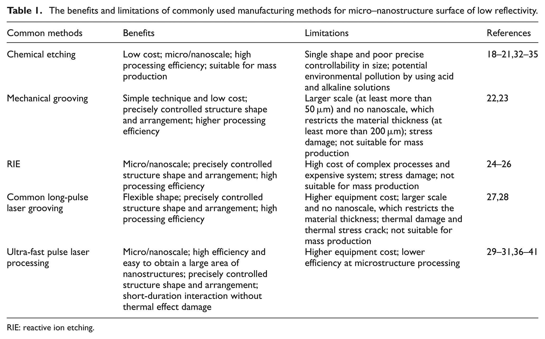
Various research groups have published articles related to low reflectivity and high absorptivity of material surfaces for light trapping structures, especially for non-metallic material surfaces. For example, a reduced optical reflectivity and enhanced absorption was obtained using routine micro–nanostructure manufacturing methods on low-reflectivity crystalline silicon surface, as shown in Figure 1. Nishimoto et al. 45 investigated the reflectance of textured multicrystalline silicon solar cells by using chemical etching technique, based on a maskless acid etching of silicon. They found that the reflectance was dependent on the ratio of the depth and width of texture. Lu and Barron 49 fabricated nanopore-type black silicon anti-reflection layers using one-step silver-assisted chemical etching and obtained the lowest reflectivity of 0.17% over a range of 300–1000 nm with the nanopore diameter being less than 30 nm and the shortest nanopore length was less than 250 nm. Shuai et al. 50 realized high-performance broadband membrane reflectors based on Fano resonance principles in photonic crystals using magnetically guided metal-assisted chemical etching. Bender et al. 46 mechanically textured V-grooves through conventional mechanical grooving process and obtained an average reflectivity of 6.6% between 500 and 1000 nm on the surface of multicrystalline silicon. Rabha et al. 51 carried out texturization of monocrystalline silicon wafers using the mechanical grooving method and reduced the total reflectivity from 29% to 7% in the 300–950 nm wavelength range. They also used mechanical grooving method for surface treatment of multicrystalline silicon wafers, and the total reflectivity dropped to about 5% in the 400–1000 nm wavelength range. 52 Yoo et al. 53 reported large-area multicrystalline silicon solar cell fabrication using RIE and observed an average surface reflectance of 13.3% for 15 min RIE-textured samples, with the conversion efficiency of solar cell reaching 16.1%. Kong et al. 47 developed nanosized pyramid column structures on a silicon surface for crystalline silicon solar cells by RIE and obtained an average surface reflectance of 1.16% in the wavelength range of 400–1000 nm without any anti-reflection coating. Mundo et al. 54 investigated RIE plasma process–based nanotexturing on the surface of crystalline silicon by using single-step maskless method to improve anti-reflective and photovoltaic behavior. Untila et al. 48 prepared V-grooves with minimal effective reflection of 2.7% with a width of 35 µm and the lowest aspect ratio of 1.56 (height to half-width of the V-grooves) on the surface of crystalline silicon solar cells by common pulse laser grooving at a wavelength of 1.06 µm, an average output power of 16 W, and a spot of about 30 µm in diameter with perpendicularly projected onto the substrate surface.
Examples of SEM image of the morphology of the textured crystalline silicon by commonly used micro–nano manufacturing methods for structure with low-reflectivity surface. (a) SEM image of an acidic textured multicrystalline silicon wafer by chemical etching of HF:HNO3 = 12:1. (b) Cross-sectional SEM image of a 35°V-grooved texturization of multicrystalline silicon by mechanical grooving. (c) Cross-sectional SEM images of RIE-textured crystalline silicon wafer for 5 min. (d) Cross-sectional SEM image of the laser V-grooved crystalline silicon wafer.
In addition to the methods discussed above, there are many other methods for manufacturing low-reflectivity surface structure, as shown in Table 2, such as the one by Zhou et al. 55 from University of Virginia, USA, who used natural lithography with SiO2 spheres of 100-nm diameter and an inductively coupled plasma to etch the surface of 4H-SiC to obtain the texture with an anti-reflective layer in a wide-spectrum range, the normal incident reflectivity of the surface was less than 5% over a wide-spectrum range from 250 to 550 nm. Choi et al. 56 from Massachusetts Institute of Technology, USA, presented and experimentally demonstrated a novel method of multiple shrinking mask etching to fabricate silica nanocone arrays with ultra-high aspect ratio of about 7 for multifunctional surfaces having excellent self-cleaning, anti-fogging, and anti-reflective properties. Guerrero et al. 57 developed a new bottom anti-reflective coating that can be incorporated into multipatterning lithography schemes by using scanner track–only processing, and the most promising anti-reflective process produced 110-nm-deep trenches with approximately 1:1 space ratio. Kettle et al. 58 from the United Kingdom fabricated anti-reflective structures with reflectivity below 6% by using a low-temperature thermal nanoimprint lithography for low band gap flexible organic solar cells. Lee et al. 59 successfully demonstrated a novel fabrication method for an anti-reflective plastic lens with millimeter-sized structures for various illumination and imaging applications by using plastic duplication with a nanoporous aluminum oxide template for a two-step anodization with lens curvature which obviously increases the transmittance and significantly reduces reflectivity. Choi and Huh 60 from South Korea reported a one-step processing method to fabricate a hierarchical dual-scale biomimetic structure for a transparent anti-reflective, self-cleaning surface layer with light transmission in organic solar cells by using the template-mediated ultraviolet (UV) replica mold to directly produce a multifunctional surface with an acrylate-functionalized perfluoropolyether without complicated fabrication steps. The surface exhibits superhydrophobic characteristics and self-cleaning properties with an obvious improvement of photovoltaic power conversion efficiency by about 10% as a result of transmittance enhancement and reflection suppression. Dasgupta et al. 61 from Stanford University, USA, reported the highest value for nanowires over the recent years and fabricated the metallic NixSi nanowire arrays for anti-reflective electrodes in organic photovoltaics by a simple, low-cost, and bottom-up method based on the thermal decomposition of silane without the need for catalysts, etching, or lithography on the surface of flexible Ni foil substrates, and the optical properties of these nickel silicide nanowire arrays showed broadband reflection suppression to levels below 1% from 1100 to 350 nm. Dhamodaran et al. 62 grew GaN nanoflowers on diverse commercial substrates by a ordinary catalysis-free chemical vapor deposition (CVD) technique; the normal incident reflectivity on the nanostructures revealed a very low reflectivity of 5%, and the wettability of the surface for the static contact angle of water-drop showed the maximum hydrophobic nature with a large static contact angle of about 145°. Cho et al. 63 proposed and demonstrated a metal-dielectric thin film with high absorption and low reflection over the entire measured visible spectrum. The thin film consisted of SiO2, Cr, SiO2, and Al layers successively deposited on glass substrate, and the total thickness of the film was only about 220 nm. Measured absorbance and reflectance of the film were 99.3% and 0.7%, respectively, with an average throughout ranging from 380 to 780 nm. This thin film became the thin black film with high absorption across the entire measured visible spectrum with both high-contrast characteristics and broadband anti-reflection.
Other methods of manufacturing low-reflectivity surface structure.
UV: ultraviolet; CVD: chemical vapor deposition.
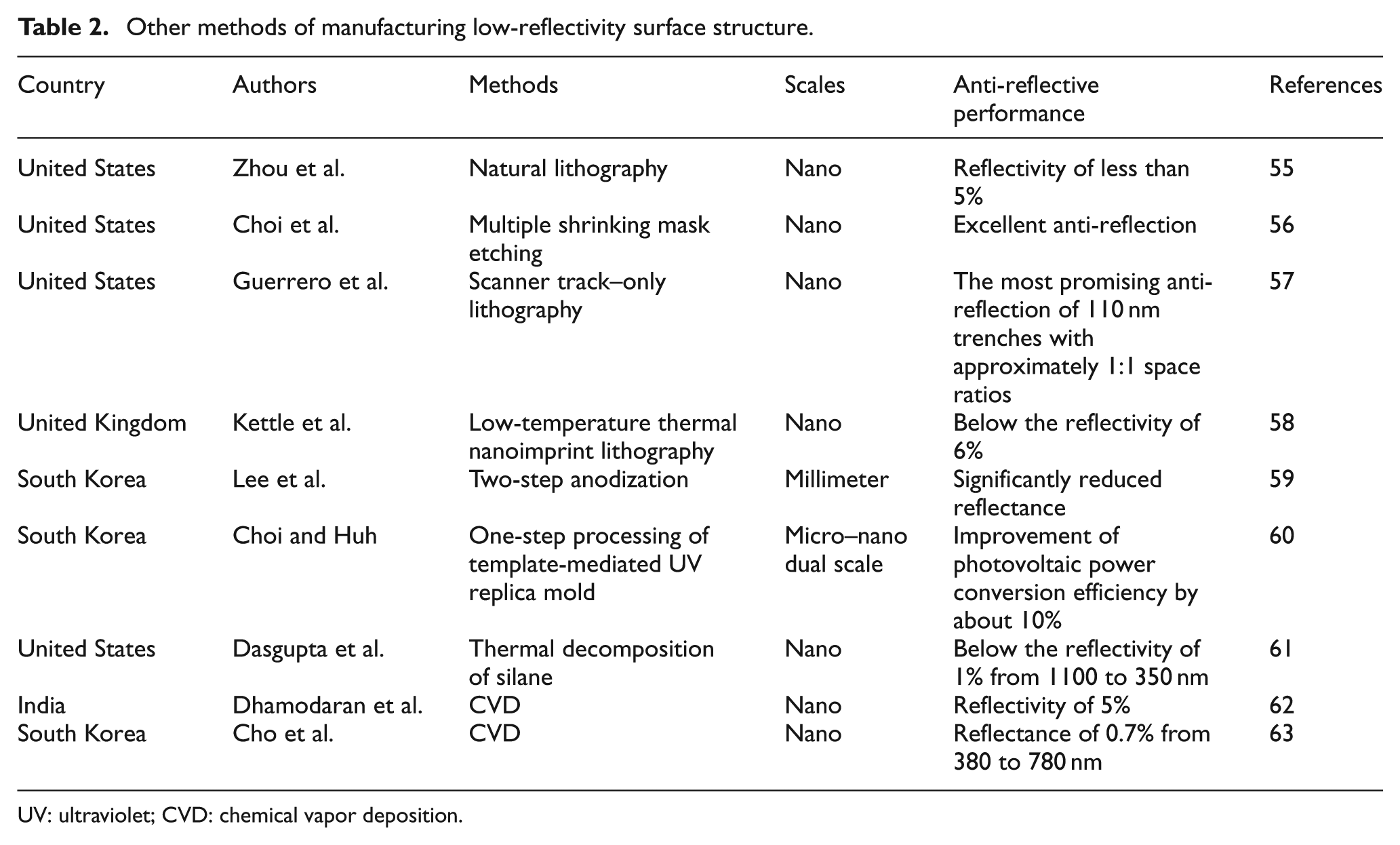
The research of micro–nano light trapping structure for low reflectivity and high absorption rate of non-metallic material surface with ultra-fast pulse laser manufacturing technology has also been presented in literature reports over the recent years. Zuev et al. 38 fabricated optimal black regimes for uniform nanotexturing of a multicrystalline silicon surface by nanosecond pulse laser radiation and produced the laser-textured black multicrystalline silicon samples with the reflectivity of 2%−3% throughout a wide spectral region. Dobrzański et al. 39 proposed a method of laser texturization, which is a common process for suppression of light reflection losses in solar cell manufacturing and investigated the microstructure of laser-textured multicrystalline silicon surface used for solar cells. The loss of light reflection was greatly reduced in their work, and the solar cells’ efficiency was 2.4% higher in comparison to untextured cell surfaces’ improving performance of the solar cells. In the process of research to study femtosecond ultra-fast laser interaction with matter, Mazur research team 64 from Harvard University, USA, found that silicon surfaces developed quasi-regular arrays of sharp conical spikes with the same crystallographic orientation as the bulk silicon while irradiated by 500 laser pulses of 100 fs duration and 10 kJ/m2 fluence in SF6 at a pressure of 500 Torr. The orientation always points along the incident direction of laser. These nanospikes had about 90% of the absorption rate in the wavelength of 300–2500 nm and change the silicon to “black silicon” (as shown in Figure 2(b)). Halbwax and colleagues40,41 also used femtosecond laser on a silicon surface to obtain a similar “penguin”-shaped nanostructure with the photocurrent of silicon solar cells increasing by more than 30% in the laser nanotextured zones (as shown in Figure 2(a)).
Examples of micro–nanostructures for light trapping with low reflectivity on non-metallic material surface with ultra-fast pulse laser manufacturing technology. (a) SEM image of penguin-like structures created by femtosecond laser (top left corner is a picture of a real penguin colony in Antarctica, photograph by Guillaume and Jennifer Dargaud (www.gdargaud.net); top right corner is a real sample photograph of a laser-structured silicon (penguin-like)). (b) SEM image of sharp conical spikes produced on silicon by 500 laser pulses of 100 fs duration and 10 kJ/m2 fluence in SF6 at a pressure of 500 Torr viewed from the surface normal (bottom left corner is parallel to the surface).
Many scholars have also carried out research related to micro–nano light trapping structures for low reflectivity and high absorption rates for metallic material surface with ultra-fast pulse laser manufacturing technology. For example, Teperik et al. 14 found that the distributed nanoporous metal surface can absorb almost all the incident light through theoretical study. Coyle et al. 65 from the United Kingdom pointed out that the light absorption rate was easily tunable by changing the nanoscale structure. These results confirmed that the nanostructured treatment of metal material surface could effectively increase the absorption rate and decrease the reflectivity to achieve effective absorption of electromagnetic waves with accurate information acquisition to make full use of light energy. As shown in Figure 3, Vorobyev and Guo66,67 produced technologically advanced black titanium alloy, black gold, black tungsten, and black platinum with absorbance of about 85%−95% throughout a broad wavelength range from infrared to UV by using a femtosecond laser pulses processing technology, which have low reflectivity. And they performed a shot-to-shot comparison research of the platinum metal absorption change in vacuum and air, which indicated that the blackening process for the platinum metal is more efficient in vacuum. Their research team has carried out research work over several years focused on the preparation and optical property evolution of nanostructure on all kinds of metal surfaces.68–72 They fabricated a group of parallel microgroove structure in the titanium metal surface by using the femtosecond laser scanning method with the absorption rate of 4.2 THz wave (70 µm) increased by 51%. Through the optimization of microgroove structure characteristics, the titanium metal surface can obtain a higher absorption rate for terahertz and sub-millimeter wave. Singh et al. 73 from University of Nebraska–Lincoln, USA, studied femtosecond pulse laser–induced modification of surface structure and optical properties of gold and aluminum and found that a low-reflection surface was formed by optimized ablation parameters for the two metals over the wavelength range from 0.3 to 50 µm. That is to say, laser ablation can form a unique surface structure with micro–nanosized features to obtain the “black gold” and “black aluminum” metal surfaces. Nayak et al. 74 from University of Virginia, USA, formed a regular array of sharp conical nanotextured microstructures on the titanium metal surface irradiated by ultra-fast pulse laser of 130 fs duration time and 800 nm centered wavelength in 100 mbar He, or in vacuum, the microstructures were over 25 µm tall, and the tip diameters of taper were about 500 nm, which greatly reduced the surface reflectivity throughout the entire visible spectrum. Tang et al. 75 from the United Kingdom formed homogenously distributed and highly organized microstructures by using the nanosecond laser pulses of 12 ns processing of copper at the wavelength of 532 nm and fabricated a large-area black copper with the surface absorbance of over 97% between 250 and 750 nm, and a broadband surface absorbance of over 80% in the wavelength range of 750–2500 nm, which has a low-reflectivity surface in the broadband range.
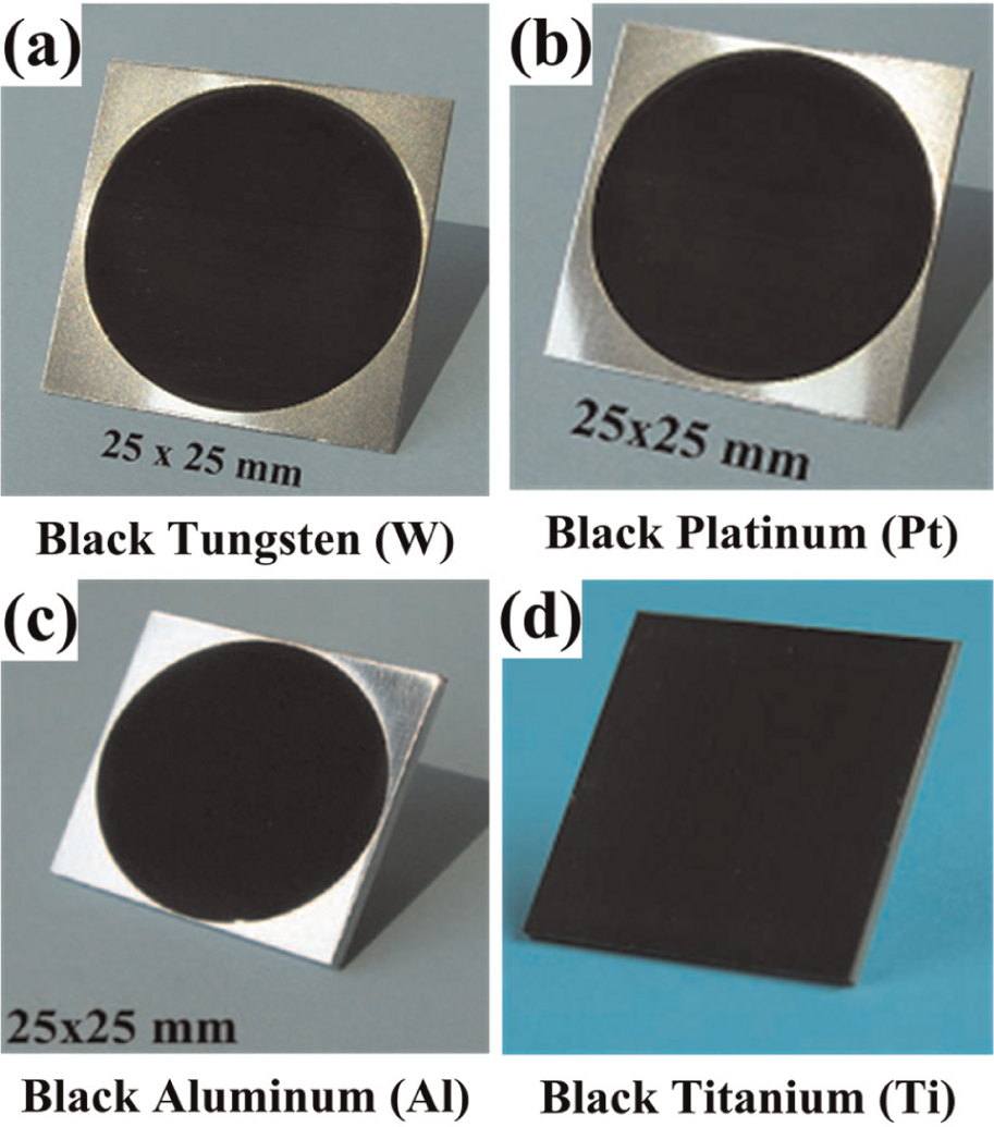
Examples of photograph of the black metal samples after femtosecond laser pulses processing: (a) black tungsten sample, (b) black platinum sample, (c) black aluminum sample, (d) black titanium sample.
Research status in China
Compared to worldwide research efforts, Chinese research of micro–nano manufacturing technology for wideband wave-absorbing light trapping structure is still in its infancy, and the research of micro–nanostructure optimization for wave-absorbing light trapping structure has not been reported, while it is seldom in the ultra-fast laser micro–nano fabrication. There exists a certain gap between the research level of China and the research being conducted outside China. Li et al. 76 from Chinese Academy of Sciences prepared an anti-reflective surface–coated calcium fluoride in the spectral range of 170–230 nm by the thermal evaporation method for applications in diffusely tunable deep UV diode-pumped solid-state laser. The reflectance of an anti-reflective fluoride coating in thickness 3 mm was measured to be in the range of 4.2% at 170 nm to 2.9% at 230 nm, with the minimum residual reflectance of 0.04% and the maximum transmittance of 99.2% appearing at 195 nm. This method significantly improved the transmittance and reduced the reflectivity. Zhang et al. 16 from Chinese Peking University reported the fabrication and optical characteristics of large-area broadband anti-reflective micro–nano dual-scale structures; fabricated microstructures by anisotropic wet etching on the surface of silicon, including V-shaped grooves and inverted pyramids, with controllable feature sizes (e.g. depth, width, and pitch); and then formed highly dense arrays of high aspect ratio nanostructures atop the microstructures by an improved maskless deep-RIE process. These micro–nano dual-scale structures further reduced the optical reflectivity to less than 0.6%, and the total light absorbance reached 95%, forming the micro–nano composite structure of the black silicon surface. Wu et al. 77 from Chinese Beijing Normal University prepared nonuniform and asymmetrical one-dimensional Si nanostructure arrays, with lengths of 1.5–7.6 µm and diameter ranging from 80 to 300 nm; the average reflectance obtained was less than 1% below 1000 nm wavelength. Yue et al. 78 from Chinese Nanjing University of Aeronautics and Astronautics fabricated anti-reflective pyramid nanostructures on the surface of silicon wafers in a RIE system at room temperature without any negative voltage pulses and obtained the reflectance of 4.72% in the wavelength range of 400–800 nm under etching time of 20 min. Yang et al. 79 from Chinese Nankai University investigated the enhanced absorption properties in the wavelength range of 0.2–25 µm for nickel–titanium alloy targets structured by femtosecond pulse laser in air and produced three different types of surface microstructures with varying pulse laser fluences. Measured surface absorbance of these microstructures was improved greatly over the broadband wavelength range from mid-infrared to UV region.
Application prospects
Special micro–nano light trapping structures fabricated on material surfaces can obtain many excellent characteristics, including a large specific surface area, low reflection and good absorption of electromagnetic waves, high energy absorption, high heat exchange capability, and heat dissipation potential, with a wide range of application prospects.80–82 The micro–nano manufactured surfaces of semiconductor materials used for light trapping structures with low reflectivity have a high absorption rate of the incident light energy and in certain cases can even fully absorb the light energy. This is particularly useful in improving the photoelectric transformation efficiency of solar cells. Metal material surfaces also have a high absorption rate of light energy, can fully absorb the light energy, and are typically used to improve the photo-thermal conversion efficiency of solar water heater. In addition, the micro–nano light trapping structure with wideband low reflectivity of material surface can be applied to absorbing the electromagnetic waves incident on building material surfaces. This improves the environmental protection consciousness by isolating continuously aggravated electromagnetic pollution. Also, it weakens signal reflection from the surface of mechanized equipment or even makes the signal vanish. Thus, effective information acquisition was implemented. And this structure also can be applied to high-radiation heat exchange equipment, solar heating equipment, solar air conditioner, and so on.
Application to solar cells
The basic principle of transforming solar energy into electricity is the photovoltaic effect. Solar cells with photovoltaic effect of silicon-based semiconductor materials are currently one of the most potential sources for renewable energy utilization.2,3,82–84 Solar photovoltaic technology is being developed for more than half a century, starting with the first practical silicon solar cells developed in the 1950s; solar cells entered into space applications in the 1960s and into the ground applications in the early 1970s, with its development continuing to the present day. According to the 2010 British Petroleum (BP) Statistical Energy Survey, the annual output of the world’s solar cells module was more than 4.6 GWP, and the world cumulative installed capacity of various solar energy photovoltaic system for the deployed applications has been more than 22.9 GWP. Solar power capacity is growing at an average of 30%, to the middle of the 21st century, which will account for 15%−20% of the world’s gross actual power generation, more than nuclear power, and is becoming one of the basic energy sources.83,84
However, the low photoelectric conversion efficiency and cost of solar cells restrict its rapid development. The main cause for low photoelectric transformation efficiency of solar cells lies in the light loss, mainly related to surface light reflection loss, loss of electrode material, transmission loss of the wafer, and so on.2,84 While the micro–nano light trapping structure manufacturing of low-reflectivity surfaces is one of the effective ways to reduce the reflection loss in solar cells. We can process the micro–nano light trapping structure with low reflectivity and high absorptivity on the material surface of solar cells by using previously mentioned various manufacturing methods. As mentioned before, these methods increase material surface roughness and effectively reduce the light loss by minimizing surface light reflection to achieve the light trapping properties of the interface. This overall improves the photoelectric transformation efficiency of solar cells and solves the performance, efficiency, and cost issue for solar cells. In the previous reviewed commonly used techniques, the problem of cost can be solved by using chemical etching or mechanical grooving to process the light trapping structures on the material surface. Chemical etching methods, however, form structures of a single shape and have poor controllability, which limits improvement in photoelectric conversion efficiency. Mechanical grooving methods fabricate structures at larger scale and without nanoscale features and also have limited improvement capacity for photoelectric conversion. The photoelectric conversion efficiency can be significantly improved by using either RIE or ultra-fast pulse laser processing to produce the micro–nano light trapping structures with low reflectivity on the material surface, but the equipment cost is relatively high. As we can see, based on analyzing the pros and cons of the manufacturing methods, there is no one best way to resolve and achieve both high photoelectric conversion efficiency and reduced manufacturing cost. Hence, research efforts should be focused on methods to improve the efficiency and reduce cost of photovoltaic systems. This can be achieved by taking advantage of available government financial incentives, which can be used to encourage citizens for photovoltaic power installations.83,85
Overall, the micro–nano manufacturing of material surface for light trapping structure with low reflectivity has important application prospects in the field of solar cells.
Application to solar water heater
Solar water heaters are presently one of the most popular and commercialized solar energy utilization devices with significant effects in the developing world.80,84,86–88 The core component of flat-plate solar water heater is a collector; it is an important device for absorbing solar radiation and converting radiant energy into heat energy, and its basic structure consists of solar panel (absorber), transparent cover plate, thermal insulating layer, and a shell. When the incident light energy strikes the heat absorption plate at a certain angle, due to the spectral selectivity of plate, almost all the wavelengths in the short wavelength of solar heat radiation are absorbed. 89 Due to thermal radiation, the temperature of the plate is far below the surface temperature of the sun; the thermal radiation of the plate belongs to long-wave radiation. The plate with long-wave radiation has extremely low reflectivity, to increase the absorption rate of the solar collector and reduce heat loss due to radiation. The wavelength range of the solar spectrum distribution does not overlap substantially with thermal radiation, so as to achieve the best solar–thermal conversion. A large surface area of the material absorbs the light in the solar spectrum, with a high absorption rate and low radiation loss in the wavelength range of thermal radiation with low reflectivity.90,91 Radiation energy is related to the types, properties, and surface state of the object, whereas the absorption rate is associated only with the properties and surface state of the object along with variation in the wavelength and intensity for the incident radiation energy.
If the panel of solar collector uses the plate with micro–nano light trapping structure with metal (aluminum) surface, there will be both multiple reflection and multiple absorption events, when incident light strikes the surface of the solar collector. The thermal absorptivity of the solar collector is significantly greater than the thermal absorptivity of material surface resulting in an improvement in the performance and heat absorption efficiency of the collector. Based on this, the micro–nano porous structure obtained on the material surface of solar water heater by using previously mentioned manufacturing methods can reduce the reflectivity of the surface and improve the solar water heating.92–94 It can promote wide application of solar water heater in real life.
Therefore, micro–nano manufacturing of material surfaces with light trapping structures and low reflectivity have important application prospects in solar water heater.
Application to building wave-absorbing materials
With the rapid development of electronic technology, electronic products, especially the popularization of mobile communication, computer, and household electrical appliances, people’s living environments are suffering from serious pollution due to electromagnetic waves. Along with the enhancement of people’s environmental protection consciousness, reducing electromagnetic pollution has been a widespread concern, and the use of microwave-absorbing materials on buildings surface is an effective way to reduce electromagnetic pollution.95,96 Now, its application has been involved in many fields of electromagnetic compatibility, computer security, anti-electromagnetic radiation, and so on. 97 According to different requirements for many different kinds of building materials, more research on the building materials for wave absorption and radiation control with applications expanding continuously, and their performance requirements increasing. While the rapid development of electronic technology, wave-absorbing materials require an increasingly wide operating frequency range. For wideband, building wave-absorbing materials are mainly used in anechoic chamber, which have a high thickness, but also very costly and difficult to apply to a wide range of applications. A significant reduction in cost is one of the key problems that need to be resolved for the application of wave-absorbing materials in buildings, especially for civilian applications.
Micro–nanostructured material surfaces have a wide range of effects on reflection and absorption within a frequency range and can have superior performance. This problem can be well solved by using previously mentioned various manufacturing methods of micro–nanostructure with low-reflectivity surfaces. Compared to other building wave-absorbing materials, the material surface of porous structure has the characteristics of large use and low cost.98–100 Current wave-absorbing materials offer a wide range of performance characteristics capable of absorbing microwave, infrared, and acoustic waves primarily used in the military. Whereas wave-absorbing, sound absorption, and insulation are primary requirements in civilian applications. We can process a micro–nano porous structure onto the material surface of the building wave-absorbing materials by using previously mentioned manufacturing methods which can solve multi-band and multifunctional requirements of buildings.101,102
Therefore, the micro–nanostructures with wideband low reflectivity using metal or composite material surfaces can be applied to building material surfaces, which is a good method with important applications to improve the absorbing performance of electromagnetic waves on building material surfaces.
Application to information acquisition of mechanized equipments
Due to rapid development of technology and need to gain information, there are competitors in all sectors resulting in industrial, commercial, and government espionage. To gain access to the relevant information from competitors, many mechanized equipments are faced with external signal detection. These mechanized equipments need to be protected against electromagnetic radiation preventing the detection of signals from outside due to signal reflection which could result in loss of private information to competitors. There is also a need to absorb electromagnetic wave signals from outside; this allows acquisition of information from competitors to gain competitive advantage. It is important to avoid private information loss to competitors. 103 The information acquisition away from mechanized equipments mainly includes the design of the surface shape and material selection to absorb detection signal, 104 which weakens or prevents reflection of signals defeating the purpose of information acquisition and camouflage or shelter the equipment from information loss. So, with an intention to improving the ability to gain information and acquire an information edge over competition, it is better to protect from information loss and allow to effectively compete against the opposite side.
Based on this, the method for special structural treatment to change material surface shape for mechanized equipments is a very important information acquisition method. This method directly changes the physical structure or morphology of material surface to increase the material’s surface roughness, significantly reduces reflection characteristic of signals, and achieves the high absorption rate for optical signals. For example, Zhang et al. 105 from Chinese Nankai University have processed compact textures into porous structures based on the theory of effective media to achieve the high absorption mechanism of infrared wave signal and improve the low-reflection characteristics of the signal itself. In some cases, the strength and other properties of the base material need to be maintained, so we can process the micro–nano porous structure or other structure on the material surface of mechanized equipments by using previously mentioned manufacturing methods to improve the wave-absorbing properties. For surface porous structure, pore size, relative density, and thickness are important factors influencing the performances of porous materials. 102 Surface porous structure material does not only have the characteristics of small environment impact but also can effectively realize both multiple reflection and multiple absorption on the material surface of porous structure, thereby greatly increasing the effective absorption coefficient.
Therefore, the micro–nano manufacturing of material surface for wave-absorbing structure with low reflectivity has important application prospects in the field of mechanized equipments’ manufacturing.
Application to high-radiation heat exchange equipment
High-radiation heat exchange equipment is widely used in the petroleum, chemical, power engineering, food industries, and so on. In the face of this global energy shortage problem, effectively taking advantage of high-radiation heat exchangers to enhance heat transfer capacity and reduce equipment investment and operation cost is the focus of continuous research.106,107 Since the 1960s, it is known that the heat transfer process can be enhanced by changing the shape or property of the heat exchange equipment surface to improve the overall efficiency of the heat exchanger.108,109
Due to the surface of porous structure enabling high-efficiency boiling heat transfer, low differential temperature boiling, high critical heat flux density, and good anti-clogging capability, it has wide industrial application prospects in heat exchange equipment.110–113 We can process the micro–nano porous structure on the material surface of high-radiation heat exchange equipment by using the previously mentioned manufacturing methods for micro–nanostructures on low-reflectivity surface. The metal surface of radiation pipes or radiation walls with micro–nano porous structure can be utilized for heat transfer to improve energy efficiency. If we provide a vertical solid wall surface with high surface porosity with micro–nano porous structure along the hot gas flow path, most of the gas heat will convert to a solid thermal radiation heat, thus the formation of a large heat drop points to the upstream of fluid movement. Since the space is surrounded by porous walls in the case of application for heat exchange equipment such as a heating furnaces or radiator, there exists a strong radiation field. This solid wall with uniform temperature distribution can evenly heat the object. The porosity of wall can be set by using various structures such as rectilinear, curvilinear, single-layer, multilayer, and honeycomb sandwich structure, to improve performance of high-temperature gas radiation heat transfer. Normal high-temperature ceramic, foam ceramic, ceramic fiber, alloy fiber networks, and specialty metals can be used for this application. 114
Therefore, the micro–nanostructure manufacturing of material surface with low reflectivity has important application prospects in the field of high-radiation heat exchange equipment.
Application to solar heating equipment
Energy consumption in buildings represents a large share of global total end use of energy. 115 Heating system and lighting system consume about 40% and 15% of the total use. 116 Residential and commercial buildings require approximately 35% of the total energy used. 115 In addition to this, energy is also used to power buildings in the industry. Globally, buildings account for nearly 40% of total end use of energy.115–117 In view of the increasing energy cost, it is of great interest that government mandates for energy efficiency, the rising human comfort requirements, and controlling natural ventilation to make effective use of natural resources can reduce energy consumption.116,118 In addition, greenhouses can also provide a suitable microclimate for various crops and protect them from severe and variable outdoor weather conditions. 119 However, in cold climate, the greenhouse structure for human and crops is usually not sufficient to keep the inside air temperature at an appropriate level, so auxiliary heating systems are required. Solar heating equipment can be used in these cases.119–121 Energy storage can make it possible to use the solar heating equipment to collect energy in the daytime for space heating when is required.
According to the different heating methods, solar heating equipments are classified into two kinds: active and passive.84,119,122–124 Active solar heating refers to the heating system that requires the installation of a solar–thermal collector on top of buildings, and placing storage tank (water as the heat transfer medium systems, thermal storage medium is hot water; air as the heat transfer medium, thermal storage medium is pebbles) and the conventional radiator in the interior, the heat transfer medium is transported by the water pump or draught fan, through the pipe connection into a forced circulation. Passive solar heating refers to the heating system depending on the natural characteristics of low solar elevation angle in winter to accomplish the functions of heat collection, heat storage, and heat release using the shape structure design of the building itself; its essence is the use of solar energy–efficient buildings. If we process the micro–nano light trapping structure on the material surface of the building’s structure or the collector in solar heating equipment by using previously mentioned manufacturing methods, the absorption efficiency of solar energy and the photo-thermal conversion efficiency of heating equipment can be greatly improved to meet the needs of human comfort requirements and various crops in greenhouse environment.
Therefore, the micro–nano manufacturing of material surface for light trapping structure with low reflectivity has important application prospects in the field of solar heating equipment.
Application to solar air conditioner
Human comfortable living environment, except for the need of heating at low temperature, also needs refrigeration at high temperature. The use of air conditioning is essential in modern society. Solar air conditioners do not use Freon and have no destructive effects on the ozone layer. These solar air conditioners have attracted wide attention as they do not use electric energy, resulting in energy saving, no pollution, and long working life.120,125–127
Solar air conditioning, in general, is the use of photovoltaic technology to produce electric power to drive the conventional compressor refrigeration and heating or making a solar–thermal conversion to produce heat as energy refrigeration and heating. The micro–nanostructure for light trapping obtained on the material surface by using previously mentioned manufacturing methods can be used for solar air conditioners with the use of photovoltaic technology or photo-thermal conversion technology to produce low-reflectivity surfaces. This greatly improves absorption efficiency of solar energy and photovoltaic capacity or photo-thermal conversion efficiency for applications in solar air conditioning. For example, Cabrera et al. 127 reported use of parabolic trough micro–nano light trapping structures on the material surface of solar collectors for solar refrigeration and air-conditioning applications.
Therefore, the micro–nano manufacturing of material surface for light trapping structure with low reflectivity has important application prospects in the field of solar air conditioner.
Conclusion
It can be seen from the research status in China and abroad that the micro–nanostructured material surface can significantly improve the performance of optical transmission and greatly reduce the broadband domain reflectivity of material surface to enhance the absorptivity of wide-spectrum signal on the material surfaces. This feature has broad application prospects and research value in many fields. In this article, several commonly used methods for manufacturing micro–nano surface of light trapping structure with low reflectivity are introduced, including chemical etching, mechanical grooving, RIE, common long-pulse laser grooving, and ultra-fast pulse laser manufacture, and their advantages and disadvantages are analyzed. Among these methods, ultra-fast pulse laser manufacture is one of the relatively ideal manufacturing technologies for light trapping structure. In addition, the research status of the micro–nano manufacturing technology of structured surfaces for light trapping with low reflectivity is reviewed, and emphasis is given to the application prospects. It has important research value in many fields and finds application in solar cells, solar water heater, building wave-absorbing materials, information acquisition of mechanized equipments, high-radiation heat exchange equipment, solar heating equipment, solar air conditioner, and so on.
For the research of the micro–nano manufacturing technology for light trapping structure with low reflectivity of material surface, although there are some research achievements from laboratory appearing at home and abroad, it is seldom on the research of formation mechanism and control method of micro–nano light trapping structure on the material surfaces. The light trapping mechanism of reflectivity is reduced by controlling the micro–nanostructure, and this area needs further systematic research. Meanwhile, the influence mechanism of nanostructure and micro-nano composite structure on the absorption characteristics to optical wave remains to be further explored. There is currently no established mature micro–nano light trapping structure preparation technology; industrial preparation of many material surfaces and application instance still need to be practical. These material surfaces can be used for solar cells, solar water heater, building wave-absorbing materials, information acquisition of mechanized equipments, high-radiation heat exchange equipment, solar heating equipment, solar air conditioner, and so on. Therefore, the research of the micro–nano manufacturing technology for light trapping structure with low reflectivity of material surface has an important scientific significance and practical application value in the field of solar cells, solar water heater, building wave-absorbing materials, information acquisition of mechanized equipments, high-radiation heat exchange equipment, solar heating equipment, solar air conditioner, and so on.
Footnotes
Declaration of conflicting interests
The authors declare that there is no conflict of interest.
Funding
This work was supported by the Major Research Plan of the National Natural Science Foundation of China (grant no. 91123024), the Development Program for Changjiang Scholars and Innovative Research Team in University of Ministry of Education of China (grant no. IRT1172), and the Fundamental Research Funds for the Central Universities of Ministry of Education of China (grant no. xjj2012113).