
Abstract
This article discusses an overview of microforming, microcasting and microwelding processes. In the case of microforming, the processes reviewed are micro deep drawing, microforging, microextrusion, microrolling, microstamping, microhydroforming and incremental microforming. This section also throws some light on how the lasers have been used for microbending and micropunching purposes. The work done in the area of physics of microforming processes has also been discussed briefly.
This article also deals with different types of microcasting processes particularly permanent mold and investment microcasting processes. The applications of these microcasting processes have been specified in different fields of engineering, biomedical and so on. Some areas in which further research work is needed have been identified. It includes both theoretical and experimental works which need attention. The last part of this article deals with microjoining in general and laser microjoining in particular. This section discusses the types of the lasers that are being used for microjoining purposes. The process parameters (laser, optics, system and material) have been explained, and some work done on the parametric analysis has been reported briefly. Various applications of laser microjoining have been elaborated before the last section on concluding remarks. This last section presents, in very brief, the areas in which further work is required in microjoining processes.
Introduction
In continuation to Micromanufacturing: A Review—Part I, this article as Part II deals with the review of some of the micromanufacturing processes, which could not be covered in Part I due to space constraint. This article reviews the processes, namely, microforming, microcasting and microjoining (MJ). In this article, an attempt has been made to present a review of the available literature related to these micromanufacturing processes. Their weaknesses and the directions for future research work also have been indicated.
The last decade saw significant progress in the development of microforming setups. It is noted that mere scaling down of macroforming setups is not enough. Due to relative higher precision requirements, different types of actuators and measurement devices are needed. Moreover, flow stress and friction behavior in microforming are different from macroforming. Nevertheless, a proper design of microforming system can provide an economic means of mass manufacturing. Nonconventional microforming processes are laser-based forming and incremental forming. These processes have provided promising applications, but their industrial applications need to gain popularity. There is still ample scope for developing efficient microforming setups, and modeling and optimization of these processes. The precision and optimization issues should be micromaterial specific. It is better to consider both metallurgical and mechanical aspects in microforming. Some of the issues have been discussed in the following sections.
Microcasting is a challenging task from many points of views as is obvious from various references cited in this article. The work done related to microcasting can be categorized as permanent mold microcasting and investment microcasting, for example, vacuum microcasting and centrifugal microcasting. This article discusses the work related to theoretical as well as experimental investigations including parametric analysis, castability, mold filling and thermal issues. Finally, some applications and concluding remarks are presented.
The last section of the article presents classification of joining processes with a special emphasis on laser MJ processes. It elaborates available literature related to the types of lasers for MJ processes, laser MJ system and their limitations and their characteristics. Transmission welding by an incremental scanning technique (TWIST) and stepless high speed accurate and discrete one pulse welding (SHADOW) are briefly discussed. Relevant process parameters and their effects on the principal responses are brought out in section “Process parameters.” The applications of laser joining in different fields including engineering are also discussed. Some concluding remarks along with possible fields of research in laser beam MJ are brought out.
Microforming
Microforming can be defined as the process of manufacturing a part or a feature by plastic deformation, whose at least one orthogonal view can be enclosed in a square of 1 mm size. 1 Microforming is also defined 2 as the production of parts or structures with at least two dimensions in the submillimeter range. The small-sized components are used in microsystem technologies and microelectromechanical systems (MEMS). Typical examples for such components are pins for Integrated Circuits (IC) carriers, fasteners, microscrews, lead frames, sockets and various kinds of connecting elements. 3 Figure 1 shows some typical microformed components, namely, gear, battery cell, cup, coin and so on. Virtually, all conventional sheet and bulk metal forming processes have been tried in their microforms. The detailed review of microforming has been presented in references.4,5 The following subsections present a brief review of some typical microforming processes. The penultimate subsection reviews the work carried out to understand the physics of the process. Concluding remarks are presented in the last subsection.
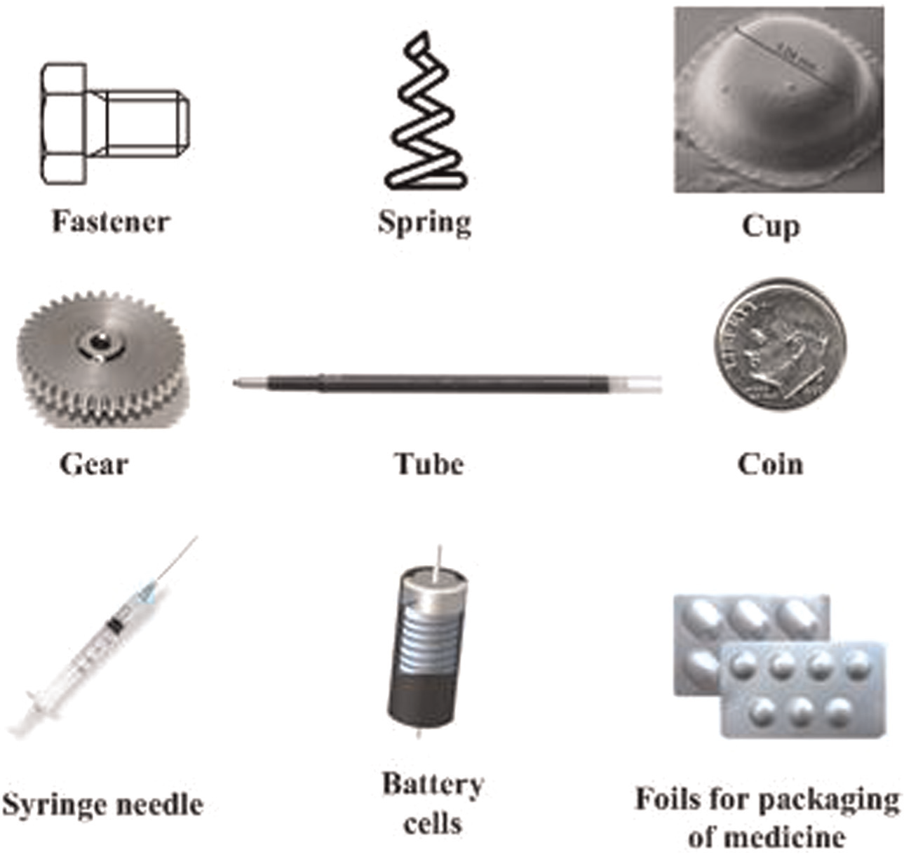
Typical microformed components.
Micro deep drawing
Deep drawing is a widely used process to produce hollow cylindrical or box-shaped objects from the sheet blank. Micro deep drawn components find extensive applications in electronic industries. However, a very high surface area-to-volume ratio during micro deep drawing enormously increases friction.
Experimental investigation into micro deep drawing has been carried out 6 using two different materials and the limiting drawing ratio was determined. Limiting drawing ratio is the ratio of the maximum blank diameter that can be safely drawn into a cup without flange to the punch diameter. It is an indicator of the drawability of the material under a particular lubrication condition and thickness. One material was Al 99.5 foil with a thickness of 20 μm and another was mild steel with a thickness of 25 μm. The punch diameter was 1 mm with a corner radius of 0.19 mm and the die corner radius was 0.12 mm. Calculations were carried out to find out punch forces in micro- and macro deep drawing. The calculated values matched with the experimental results in macro deep drawing with a punch diameter of 50 mm, but they were significantly different from the measured values in the case of micro deep drawing. This is because the average kinetic coefficient of friction in microforming is much greater than that in macroforming.
A cup of 500 μm diameter was made 7 in two stages from SUS304 stainless steel foil of 23 μm average thickness and Ra value of the surface roughness as 0.11 μm. Finite element (FE) simulation results considering the effect of surface roughness matched well with the experimental results. The effect of die cavity dimension on micro deep drawing using T2 copper foils of 50 and 90 μm thicknesses was studied. 8 The micro die cavity dimensions were found to be significant parameter.
Gong et al. 9 used diamond-like carbon (DLC) film–coated blank holders and dies to form micro cups with drawing blank diameter of 2 mm. A plasma immersion ion implantation and deposition process were proposed to treat the blank holders and drawing dies. The minimum cup diameter was 0.95 mm. It has been observed that DLC film decreases the drawing force and increases the limiting drawing ratio. It was also observed 10 that the coefficient of friction of a DLC film–coated tool against the stainless steel X5CrNi18-10 (dry friction without lubricant) is lower than that of an uncoated steel tool X153CrMoV12 against the stainless steel X5CrNi18-10 under a load in the range of 5–25 N. In the case of DLC-coated tools, no damage in the form of cracks or flaking was observed. Vollertsen and Hu 11 carried out micro deep drawing with punch diameter of 1 mm and punch velocities of 1, 10 and 100 mm/s. The maximum kinetic friction coefficient in micro deep drawing decreased with increasing punch velocity. This is in line with the observations in macro deep drawing. Using 20-μm-thick Al 99.5 blank material, a limiting drawing ratio of 1.8 was obtained. The allowable upper limit for initial blank holder pressure increases with increasing punch velocity.
Molotnikov et al. 12 experimentally investigated the effect of blank thickness on deep drawing of copper. A dislocation density-based model 13 was used for FE simulations in ABAQUS that takes into account the thickness effect. It was demonstrated that the blank thickness effect is governed by the ratio of blank thickness t to the grain size D of the material. The ratio t/D indicates the number of grains along thickness. The critical value of t/D ratio below which size effect comes into picture was determined.
Vollertsen et al. 14 manufactured two different foils of 15 μm thickness out of the Al-SiC alloy using a magnetron-sputtering process at two different temperatures (37 °C and 160 °C). These two different foils were used as blank material in micro deep drawing with a punch diameter of 750 μm to investigate formability of these foils. A limiting drawing ratio of 1.6 was achieved for both foils. Similar kinds of experiments were repeated 15 using Al-Zr alloy.
Brabie et al. 16 developed a model using Barlat’s 89 anisotropic yield criterion for the prediction of thickness variation during deep drawing of micro- and milli-parts. There was a good agreement between experimental and model-predicted results for deep drawing of the foils of 50–200 μm (punch diameter as 1 mm and drawn depth as 500 μm). Fu et al. 17 carried out experimental and simulation studies in microblanking and micro deep drawing using copper sheet. The loads predicted by simulation using ABAQUS qualitatively agree with the experimental results. When the grain size is of the order of the blank thickness, grain orientation and distribution significantly affect deep drawing process. The fraction of grain boundary increases with decrease in grain size, which leads to the increase in flow stress and deformation load.
Microforging
Saotome and Inoue 18 have carried out superplastic microforging on fine-grained superplastic Al-78Zn alloy, pure iron as a transformation superplastic material and amorphous LaAlNi, ZrAlCu alloys, which exhibit a supercooled liquid state. V-grooved microdies with a throat width of 1–20 μm made of (1, 0, 0) silicon were used. An evaluation system for microformability was also proposed. The deformation characteristics of microforging of Zr65Al7.5Cu27.5 and Zr55Al10Cu30Ni5 amorphous alloys also have been studied. 19
Microforging tests have been carried out 20 on Al 5083 alloy using Si-based microdies with V-groove and pyramidal shape pattern (Figure 2), which were fabricated by anisotropic etching method. V-groove die of 100 μm was used and the process was optimized at the following forming conditions: load = 96 N, temperature = 530 °C and forming time = 20 min.
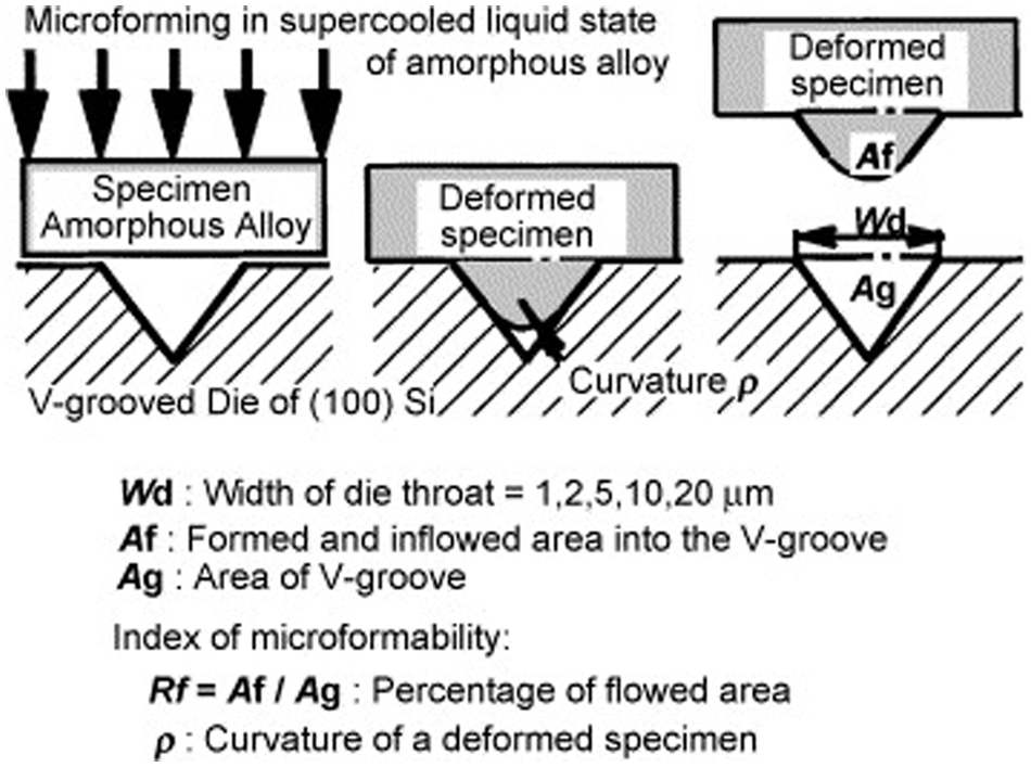
A schematic diagram of microforging with V-grooved die. 19
Hirota 21 proposed a methodology to form billets (1 mm diameter) by extruding a sheet (2 mm thick) in the thickness direction (Figure 3). Here, the punch presses the sheet at the top surface; as a result, the material from the bottom surface extrudes in a die. The billet remains attached to sheet surface and can be cut if required. The process is called as microforging. In this process, one zone in the material undergoes forging and the other zone undergoes extrusion as shown in Figure 3. Hence, the process should be called microforging/extrusion process. Ghassemali et al. 22 have proposed an upper bound method to optimize this type of microforging/extrusion process.
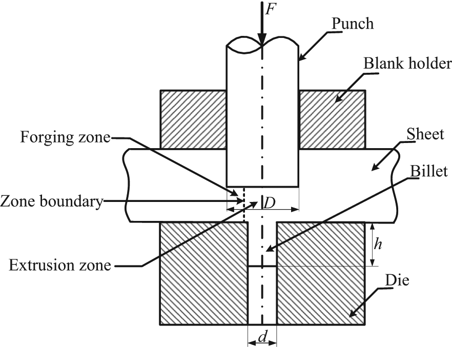
A schematic diagram of microforging process for producing billets from sheet.
Li et al. 23 have presented a three-dimensional (3D) simulation and experimental studies of sinking thin-walled copper tube with axial inner microgrooves through radial forging. An FE model is established to study deformation of grooves, distribution of equivalent stress and strain and effects of process parameters. Experimental results are compared with the simulation results. Vibration-assisted microforging of C5191 phosphor bronze 24 led to the surface finish improvement.
Microextrusion
Microextrusion is classified either as forward or backward extrusion process. Dixit and Das 1 have presented a brief review of microextrusion. It is a fast process with minimal wastage of raw material and is suitable for mass production. Saotome and Iwazaki 25 conducted backward microextrusion experiments in vacuum or organ gas environment, with arrangement for heating. The authors used La55Al25Ni20 amorphous alloy and Al-78Zn superplastic alloy to produce 10 teeth microgear shaft with module varying from 10 to 50 μm. Figure 4 shows scanning electron microscope (SEM) microphotographs of extruded microgear shafts. Krishnan et al. 26 used a novel forward microextrusion process apparatus for extrusion of brass pins with an extruded diameter ranging from 1.33 to 0.57 mm. The segmented die cavities of submillimeter size were made by electro discharge micromachining and then polished to ensure surface roughness values in the range of 0.8–1 μm. Samples used in the experiments were heat treated at various temperatures for 1 h to obtain desired grain size ranging from 32 to 211 μm. Three different extrusion dies coated with DLC-Si, CrN and TiN were used in the microextrusion experiments. The best results were obtained with DLC-Si coating. FE simulations and analytical models were then used to make comparison with the experimental data.
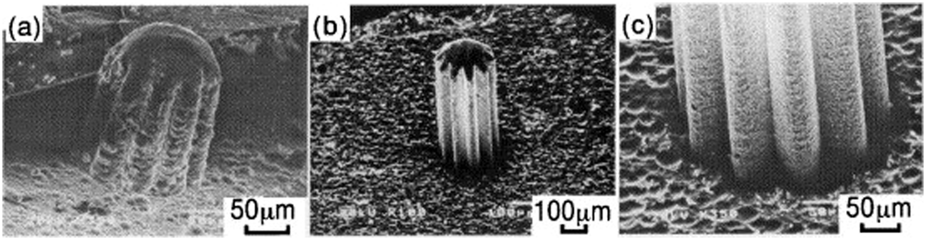
SEM microphotographs of extruded microgear shafts made of Al-78Zn superplastic alloy: (a) module 10 μm and (b, c) module 20 μm. 25
Parasiz et al. 27 studied grain size effect on bend ability and microhardness of the extruded micropins. They found that the pins extruded from larger grain size material have higher tendency to bend as compared to the pins extruded from smaller grain size material. This is because of the fact that small grain size material deforms more uniformly than large grain size material. It was observed that the pins fabricated with coarse-grained material had higher value of hardness as compared to hardness of the pins fabricated with fine-grained material. This is in contradiction to the intuitive understanding.
Cho et al. 28 developed a direct extrusion process to make microcondenser tubes of Al100 and A3003 alloys for the application of eco-friendly refrigerants with higher working pressure. Although cross section of the condenser tube is of several millimeters, there are several rectangular channels in it of cross section as small as 200 μm × 600 μm. This is an example, where the size of the product is in macro, but the features produced in it are of micro range.
Bulk metallic glass (BMG) is a class of metal alloys having an amorphous structure, better strength, corrosion and wear properties. Microextrusion experiments have been carried out 29 on Zr55Cu30Ni5Al10 BMG in its supercooled liquid state. A backward extrusion process was used at a temperature of 452 °C and strain rate of about 1 × 10⁻² s−1. A 3D cup-shaped object with wall thickness of 50 μm and outside diameter of 2.2 mm was produced. In another study, with the help of a five-hole die with an average hole-diameter of 350 μm, the extrusion of wax and lead alloy was carried out. 30 The extrusion load increases with increase in ram speed but decreases with decrease in die land length.
Microrolling
Sometimes the word microrolling is used for foil rolling or rolling of very thin strips. Kim et al. 31 developed an FE model using grain and grain boundary elements for microrolling. The experimental validation has not been carried out. Byon and Lee 32 used strain gradient plasticity to model microrolling process. The simulations were carried out for rolling of copper sheets of 1.25–12.5 μm thickness. It is noted that strain gradient plasticity predicts results different from conventional plasticity results. The validation with extensive experimental data is lacking. Yamamoto and Kuwabara 33 carried out form rolling experiments using spline dies and dimple dies for transcribing microgrooves on the surface of SUS303 and A5056 shafts of 9 mm diameter.
Microstamping
Stamping includes a number of processes, in which the sheet metal is pressed by a punch. 34 These include punching, blanking, embossing, bending and so on. Punching and blanking are different from other sheet metal forming operations, in the sense that here the removal of material takes place. In punching (often used synonymously with piercing), the portion removed from the parent sheet is scrap and in blanking the removed part is the desired product.
Kals and Eckstein 35 studied size effects in micro tensile test, micro air bending and micropunching of sheet metal. The materials investigated were copper nickel alloy CuNi18Zn20 and brass CuZn15, both in the soft recrystallized state. It was observed that physics of micropunching is quite different from the physics of tensile test and air bending. In micropunching, the minimum sheet thickness was 100 μm, the corresponding punch diameter was 2 mm and the die-punch clearance was 10 μm.
Peng et al. 36 carried out microstamping with a tubular punch, in which laser beam traverses through a hole in the punch for preheating the workpiece. Joo et al. 37 punched holes of 100, 50 and 25 μm in diameter on foils of brass and stainless steel of 100, 50 and 25 μm thickness, respectively. Taking the ratio of die clearance to workpiece thickness as 5%, the die clearance of 1 μm was needed for 25 μm size hole punching. Straightness and alignment errors were also limited to 1 μm. The punch was fabricated from tungsten carbide and a machine vision system was used for alignment. In 100 μm hole punching, the deformation behavior could be understood with conventional ductile shear fracture theory; 25 μm hole punching produced a large amount of burr with unconventional-deformation behavior. The precision fabrication of die and punch has attracted the attention of several researchers. Xu et al. 38 used ion beam irradiation for surface treatment of micropunch. Kolleck et al. 39 developed a flexible forming and punching process of stainless steel 1.4310 with a sheet thickness of 0.04 mm and tensile strength of 1200 MPa. The hole pattern with raised edges was produced. Xu et al. 40 developed a microforming system driven by double linear motor equipped with a micropunching tool and a precision automatic feeding apparatus guided by a charge-coupled device (CCD) camera-based system. Microholes of minimum 150 μm were produced by this system. Xu et al. 41 studied the size effect in microblanking and observed that fracture mechanism of brass foil is different from that of stainless steel foil. Thus, proper information about material behavior is of paramount importance for modeling a process. Blanking clearance to grain size is one of the main factors that affect deformation behavior in microblanking. 42
Springback behavior of 26000 1/2 Hard (H02) brass in three-point microbending was studied. 43 It is concluded that the conventional concept of springback cannot be applied on brass sheet (thickness <350 μm). In another study, the brass C2680 foil was selected as experimental material. 44 It was annealed to eliminate work-hardening effect and get different grain sizes. The results show that the bending force increases with increasing punch displacement. 44 With the foil of same thickness, a smaller punch radius leads to a larger bending force. When grain size increases, bending force becomes smaller.
Embossing is the process of producing raised or sunken design on the sheet by the application of pressure. Wang et al. 45 fabricated microgear of Zr65Cu17.5Ni10Al7.5 BMG using hot embossing process at 410 °C. FE simulation of the process has also been carried out.
Microhydroforming
Hydroforming is the process of forming of tubes and sheets under hydrostatic pressure. Sheet hydroforming uses a single die. The sheet is driven into the die by high-pressure liquid on one side of the sheet to form the desired shape and size. Tube hydroforming causes radial expansion of metal tube into the desired shape using two die halves. Figure 5 shows the schematic diagrams of tube hydroforming and sheet hydroforming.
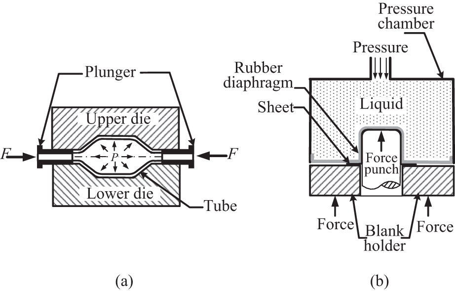
Schematic diagrams of (a) tube hydroforming and (b) sheet hydroforming.
Zhuang et al. 46 studied localized thinning in hydroforming of microtubes. The initial outer diameter of stainless steel tube was 800 μm with 40 μm wall thickness and final outer diameter as 1030 μm. Crystal plasticity FE modeling technique was implemented in the ABAQUS, while in other cases explicit FE package was used for modeling. The computational results were validated through experiments. It was observed that localized thinning is affected by microstructures and grain orientation in the material. Hung and Lin 47 designed and fabricated a sheet hydroforming machine for fabricating microflow channels for metallic bipolar plates. The system uses an intensifier that can sustain about 1230 MPa working pressure. Forouhandeh et al. 48 discussed the latest developments in microhydroforming. They carried out FE simulation, and the hydroforming experiments were conducted on CuBe 2% alloy sheet of 0.05 mm thickness. Forouhandeh 49 also microhydroformed commercially pure titanium grade 1 sheets of 300 μm thickness.
Laser-based microforming
Lasers have been used to assist mechanical forming processes to directly form the materials by thermal stresses. 50 Laser beam locally heats the workpiece and then tools made of sapphire deform by mechanical means. A laser-assisted microforming using frequency quadrupled Nd:YVO4 laser to create a microfeature on two concentric cylinders with a depth of 100 μm and diameters of 400 and 200 μm was proposed. 51 The solid-state laser created a rough surface; hence, excimer laser with a rotating mask was recommended.
In hybrid forming process, the initial shape can be formed by a conventional tool that can be corrected by laser forming. 52 It prevents springback in aluminum sheet bending. 53 Metal substrates were pre-bent to nominal shapes on a built ad hoc mold after being constrained on it. Then, they were post-treated by high-power diode laser to prevent deformation of the pre-bent sheets after the release of the constraints. Empirical and neural network modeling of the process was also carried out.
Forming of sheets by mere application of laser heat has gained profound attention in the last decade, although the process dates back to 1980s. 54 An analytical model was proposed 55 for the prediction of bend angle during laser forming, accounting for temperature-dependent properties of the material. A good agreement with experimental results was found. Otsu et al. 56 carried out microbending of thin spring by spark forming and compared it with laser forming. In spark forming, thermal stresses are generated by electric spark. A 0.5-mm graphite needle acted as one electrode and the spark was generated between graphite electrode and sheet by a charging/discharging circuit containing a capacitor. Beryllium copper, pure titanium, pure copper and 18Cr-8Ni stainless steel sheets (thickness <50 and 70 μm) were used as specimens. It is concluded that spark forming is a better method than laser forming. Labeas 57 developed an FE model with non-uniform mesh for laser forming of aluminum components. The developed model considers temperature-dependent thermal and mechanical properties of the material and a Gaussian moving heat flux.
The effect of graphite coating was found to have a significant influence on its performance. 58 Edwardson et al., 59 however, reported that irradiation damages and burns the graphite coating. Barletta et al. 60 concluded that Al2O3 coating on aluminum sheet improved the bend angle significantly. Singh 61 studied the performance of hydrated lime coating and found it better than the graphite grease coating.
In a recent development, laser-induced shock waves were used as micropunch. 62 A sacrificial coating on the workpiece was used to generate high-pressure plasma under a laser pulse. No signs of melting, burning and ablation were observed. Good quality microholes of 250 μm in diameter were punched on sheet metal of 10 μm by a single laser pulse.
Incremental microforming
Jeswiet et al. 63 defined asymmetric incremental sheet forming (AISF) as metal forming process that uses a solid, small-sized forming tool, which is in continuous contact with sheet metal and moves under control, in 3D space to produce asymmetric sheet metal shapes. The process does not have large dedicated dies. Some researchers64,65 define incremental forming in a slightly different way also.
An in situ incremental microforming system for 3D shell structures of foil material using computer numerical control (CNC) has been developed. 66 A 600-μm-long car body shell was formed. Obikawa et al. 67 developed a process of single-point incremental forming (SPIF) of thin aluminum foils, which did not require die and any backing plate. Incremental forming of arrays of dots of 0.1 mm in diameter, miniature pyramids, miniature car and miniature letters were performed under the optimized conditions at arbitrary positions on a 12-μm-thick foil. Fan et al. 68 carried out electric hot incremental forming of Ti-6Al-4V titanium sheet. Hmida et al. 69 experimentally studied the influence of initial grain size in micro-SPIF for thin sheet metals. Duflou et al. 70 used laser for localized heating in incremental forming. Although the process was used to produce macrocomponents, it can be a potential process for fabrication of microcomponents.
Severe plastic deformation processes for getting ultra-fine-grained microstructures
Severe plastic deformation (SPD) is a process to convert conventional micro-grained metal or alloy into submicrometer or nanoscaled material using very high plastic strains.71,72 Four most common SPD processes are high-pressure torsion (HPT), equal channel angular extrusion (ECAE), cyclic closed-die forging (CCDF) and accumulative roll bonding (ARB). Strains of the order of 10 are achieved and ultimate strength may reach two to three times of normal strength. The schematic diagrams of the processes are shown in Figure 6.
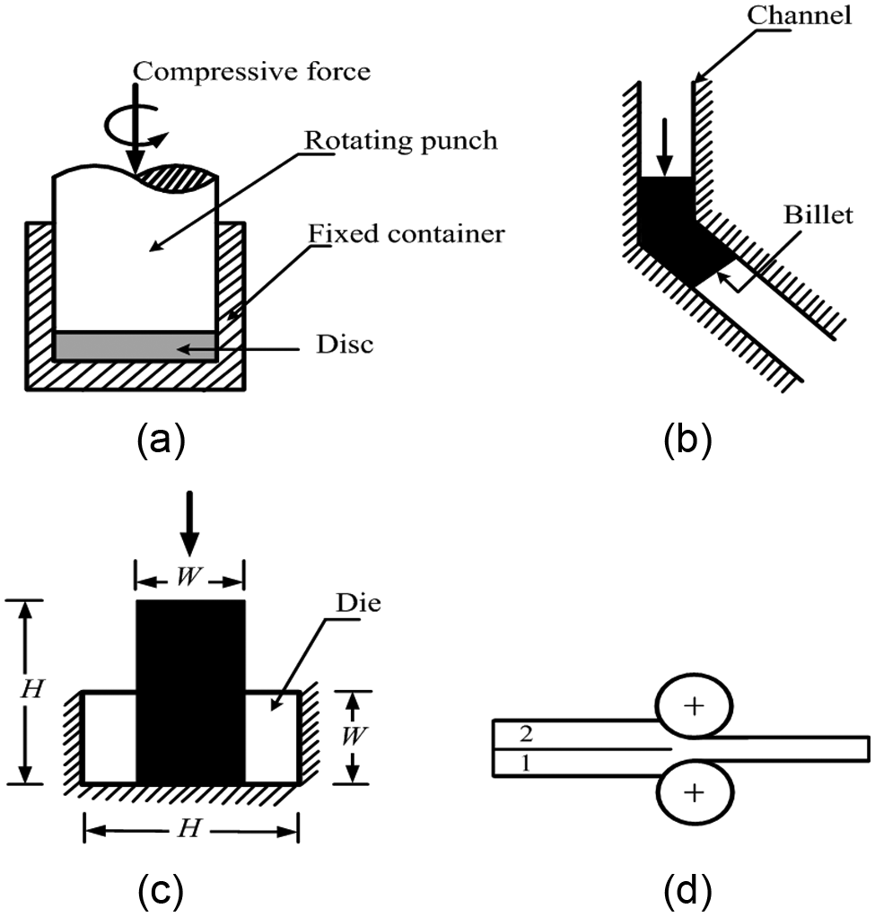
Schematic diagrams of severe plastic deformation processes: (a) high-pressure torsion, (b) equal channel angular extrusion, (c) cyclic closed-die forging, (d) accumulated roll bonding.
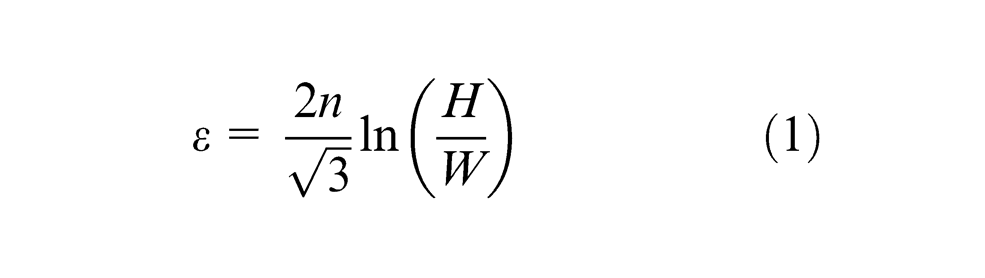
In HPT, the material in the form of disk experiences shear deformation between a fixed die and a rotating punch applying the force in downward direction (Figure 6). The process is limited to small disk. In ECAE, a billet is passed through intersecting closed channels of the uniform cross section meeting at an angle. The billet shape and size remain same, but the large amount of redundant deformation in the form of shear takes place, thus producing ultra-fine-grained structure. In CCDF, a billet of height H and width W is compressed till its height becomes W and width H. The billet is then rotated by 90° and is compressed again. In n such compressions, the average strain is given by
However, the strain distribution is not uniform. In ARB, two strips are stacked together and passed through counter-rotating rolls to achieve 50% reduction. The sheet gets pressed and deformed. The deformed sheet is cut into two pieces, both the pieces are stacked and the process is repeated. In n passes, the accumulated strain of about 0.8n is achieved. A combination of various SPD processes can also be employed. For example, Mani et al. 73 developed torsional equal channel angular extrusion (TECAE), in which the billet coming out of channel is twisted as well.
Physics of microforming processes
There have been a number of attempts to study the size effect on material flow and friction.74,75 Size effects can be grouped into three categories—density, shape and microstructure size effects. Density–size effects occur, when the absolute number or integral value of features per unit volume is kept constant, independent of the size of the object. The features could be small pores, dislocation lines or interface areas. One example of this size effect is the size dependence of the strength of brittle materials. As the probability of existence of defects (cracks, etc.) decreases with decreasing size, the strength gets increased. This effect is expected to occur in the sample of size ranging from 1 to 10 mm. However, in the size range of 100 μm to 1 mm, 75 the strength decreases with decreasing size due to the dominance of shape–size effect. Shape–size effects are related to the surface area and volume. When shape is kept constant, due to the reduction in the size of an object, the ratio between total surface area and volume increases, because the volume of a part is proportional to the cube of its size, while the surface area is proportional to the square of its size. As per surface layer model theory, 3 the grains located at free surface are less restricted than the grains located inside the material. Therefore, it leads to less hardening and lower resistance against deformation of the surface grains and makes the surface grains to deform more easily than grains inside the material. For the same grain size with decreasing size of the specimen, the share of surface grains increases, which results in decreasing flow stress of the material.
Following mathematical model for predicting flow stress as a function of grain size and shape of the specimen has been proposed 76

where
Chen and Tsai 77 conducted experiments and found that the hardness of smaller piece is lower. The hardness is nearly proportional to flow stress. Hence, microindentation can be a viable method for assessing flow stress of a small part.
In microstructure size effect, microstructure features are not scaled down in the same manner as macroscopic size of the object. One example is the intrinsic material length that was introduced to include size effect in the constitutive laws. For each metal, there exists a particular intrinsic material length scale, say, for a polycrystalline copper it is 1.54 μm. Therefore, in the polycrystalline copper, the strain gradients of the order of 1/1.54 (μm)−1 are significant. The theory that takes into account the strain gradient effects is known as strain gradient plasticity. 78 This effect is usually observed in the size range of 10 nm to 100 μm. 75
The friction behavior between the die and work interface is greatly affected by miniaturization. The effect of miniaturization by ring compression test and double cup extrusion setup was investigated and it was found that the value of friction factor increases as the size of the billet decreases. 79 In an extrusion process, friction factor increased by 20 times for the reduced size when using extrusion oil as lubricant. 2 This behavior has been explained by the open and closed lubricant pockets model. Figure 7 shows an enlarged schematic diagram of open and closed pockets. The closed pockets are those which are not connected to the edges of the specimen, and they can retain lubricant during the process while others are known as open pockets. In a small component, the proportion of closed to open pockets is low. Hence, the lubricant is not retained effectively. Due to this, the real contact area between die and work material increases, which leads to increased coefficient of friction. This increases the friction force. When solid lubricants are used, the friction does not vary significantly with workpiece size. This confirms the model of closed and open lubricant pockets.
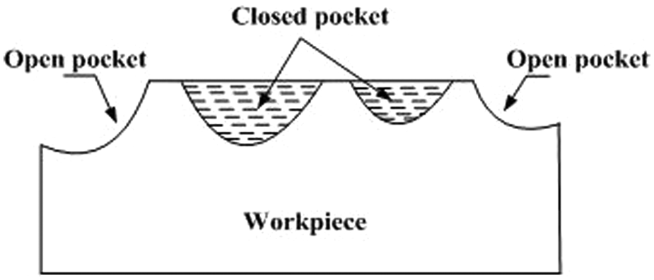
A schematic illustration of open and closed pockets.
Remarks
The research and development in microforming can be broadly classified into two categories, one based on scaling down of conventional metal forming processes and the other based on newer technologies such as laser and incremental forming. The scaling down of conventional metal forming processes requires precision in fabrication of tooling and online or offline inspection. Thus, the experimental research in microforming is closely interlinked with other areas of micromanufacturing for fabrication of precise setups. Theoretical research in microforming requires new constitutive equations and friction models. Invariably, more in-depth understanding of metallurgical aspects is required. At the same time, efficient solution techniques also need to be developed. Although, at present, the industrial applications of various microforming processes are limited, it deserves special focus on research and development front due to its several advantages. Microforming processes can be economical for mass production with high production rate. The dimensional accuracy and surface finish of microformed products are important issues to be addressed. It is also possible to obtain better mechanical properties of microformed products. Figure 8 shows a fishbone diagram depicting important factors that affect performance of a microforming system.
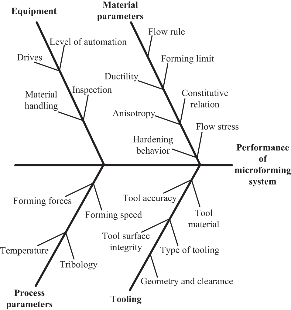
A fishbone diagram showing the input parameters and response as performance of a microforming system.
Microcasting
Microcomponents are widely used in manufacturing, biotechnology and information technology applications. They can be manufactured by various microsystem technologies, for example, the Lithographie, Galvanoformung, and Abformung (in German; translation: Lithography, Electroplating, and Molding; LIGA) technique; 80 micropowder injection molding; 81 microelectrical discharge machining; 82 wire electro discharge grinding 83 and forging, electroplating, laser ablation, micromilling and microinvestment casting. 84 These processes have limited productivity since each part has to be separately microstructured. However, limitations include applicable materials, size, shapes, capacity to manufacture high aspect ratio (AR) microparts and microstructuring inner areas. 85
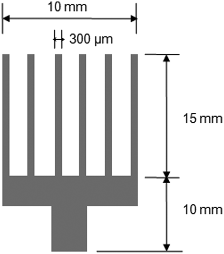
Nowadays, microcasting techniques, namely, permanent mold and investment casting85–90 are being used to manufacture microparts in large quantities. Attempts have been made 91 for mathematical modeling of microcasting processes from microscopic point of view. Microcasting is a manufacturing process for producing small structures in the micrometer range or larger parts carrying microsized structures with high AR (ratio of flow length to diameter) using a metal melt, which is cast into a microstructured mold92,93 (Figure 9). This technology has been successfully applied for manufacturing of instruments for surgery, dental devices, biotechnology, miniaturized devices for mechanical engineering applications, jewelry and dental casting. The process is capable of manufacturing very complicated structures, scalable, economically efficient for mass production and requiring minimal subsequent machining.92,94 The process can more easily fabricate structures with curved surfaces and with higher throughput than other processes. In this work, a state-of-the-art review of microcasting techniques, the current research, application areas and future perspectives is presented.
Schematic diagram of an illustrative microcasting part containing microsized features.
Methods and state of the art
Two different techniques for casting structures in the micrometer range are in use: capillary action microcasting and investment microcasting. 92 The first technique uses a permanent mold having cavities shaped by high-precision grinding. These cavities can be filled by either of the two techniques, the suction principle or the displacement principle. In the first method, melt is sucked into a specially coated mold, by capillary action. In the second method, casting alloy is melted inside a divisible mold and fills the microstructured cavities by capillary force. Subsequently, the pressure is applied to the mold to displace the excess melt through the slit. In capillary action microcasting, the castable geometries are limited to structures, which can be filled by the application of capillary forces.
Investment microcasting technique, also known as the lost-wax/lost-mold technique,87,88,92,93 does not suffer from the above-stated limitations. Here, by molding from a microstructured grand master pattern, parts of arbitrary geometry can be manufactured.93,94 An injection molded plastic master is embedded in a gypsum slip, then dried and sintered. During this process, the master is lost by melting and pyrolysis. The preheated gypsum mold is then filled with a metal melt by centrifugal force or otherwise. After removing the mold from the casting, the cast structure is cleaned and the microparts are separated from the gate system. 92 This technique has the advantage of being a simple process, giving high material utilization ratio with a possibility of casting complicated shape in large quantities at relatively low cost compared to common ultra-precision technologies.92–94 There are some important differences between microcasting and the well-known lost-wax/lost-mold process for macrocomponents. In microcasting, complex molds are used instead of shell molds that are common for bigger parts. The filling of the microstructured molds is enhanced by preheating of the mold and by applying an external force to the melt. The latter is realized in vacuum pressure casting using pressurized air at a maximum pressure of 4 bar, whereas in the centrifugal casting process a pressure of about 20–25 bar is effective. For investment casting, porous molds are needed in order to allow residual air or gas to penetrate through the wall when cavities in the mold are filled with melt. The porosity, however, affects surface roughness of the mold and, as a consequence, that of casting.86,88
Among other methods to manufacture microparts, a vacuum casting method was suggested. 95 It was reported that a conventional vacuum casting process with minor changes can be employed to fabricate microstructures, high AR structures and submicrometer features. 96 Microprecision investment casting is adapted to parts smaller than 1 mm and to bigger ones with structural details in micrometer range (Figure 10). 85 It was shown that features with size less than 150 μm, ribs with AR higher than 50 and surface roughness around 5 μm could be reproduced with an accuracy of 10% or less. Centrifugal microcasting process (Figure 11) can produce higher pressure for form filling compared to the vacuum pressure casting process. This is beneficial for casting of very small structures and long and thin fiber-like parts. 92 Centrifugal speed and preheating temperature of the mold significantly influence flow length. 85 Moreover, in this process, molds need to be designed to withstand high centrifugal force, and centrifugal microcasting parts contain higher compressive residual stresses than those produced by vacuum casting. 89 The capabilities of two different process chains, lost-wax process and direct shell process, for producing accurate castings having micro/mesoscale features have been compared. 96 The soundness, quality, microstructure and production cost of castings manufactured by employing these two processes are also discussed in detail.
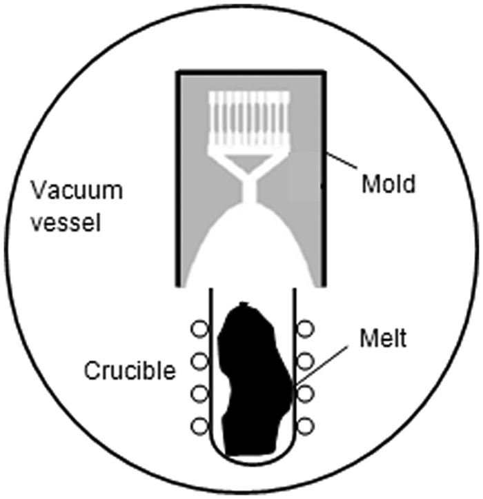
Schematic of the vacuum microcasting process.
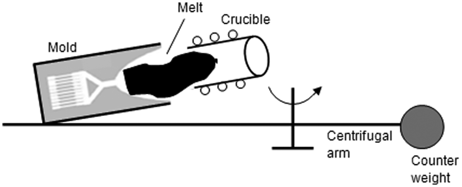
Schematic of centrifugal microcasting.
Some demonstrative examples of microcast parts are shown in Figure 12. 97 The metal was cast into flexible silicone molds that were themselves cast from microfabricated silicon templates (Figure 13). They showed that metal can be reliably cast to ridges with periodicity of 400 nm and holes or pillars with diameter in the range of 10–100 μm and AR up to 2:1 (Figure 12(b)). It is also reported that preheating of molds results in improvement in filling ability of the molds as well as coarsening of grain size in the solidified casting, say, from 30 μm to about 170 μm. 86 Baumeister et al. 87 reported that compared to phosphate bonded investment, the plaster bonded investment can be easily removed from the cast parts with very complicated microstructures without damaging or influencing chemically reactive metal. Plaster-based investments with high amounts of fine-grained quartz powder are appropriate to produce microparts with details down to the micrometer range. 88 Compared to the results achieved using commercial investments for dental casting (Ra = 1.1 μm), the surface roughness of the microparts manufactured with investments made of hard plaster and fine-grained quartz powder is significantly reduced (Ra < 0.5 μm). A microcasting technology based on integrating investment casting and centrifugal casting was investigated in Yang et al. 98 The microparts of Zn (4%) Al alloy with an AR up to 200 were produced at the centrifugal speed of 1500 r/min and the mold temperature of 270 °C. The experimental results of casting of Zn (4%) Al alloy showed that flow length increases as rotational speed and mold temperature increase. Cannon and King 84 described an investment casting process to produce aluminum molds having integrated microstructures. Unlike conventional micromolding tools, the aluminum mold was large and had complex curved surfaces. The aluminum microstructures had an AR of 1:1 and the sizes ranged from 25 to 50 μm.
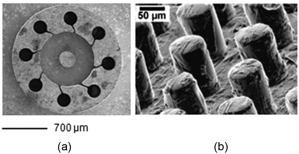
Miniaturized demonstrative microcasting parts: (a) nozzle plate with 1.9 mm diameter and 25 μm channel width made of gold base alloy and (b) metal pillars with 50 μm diameter.
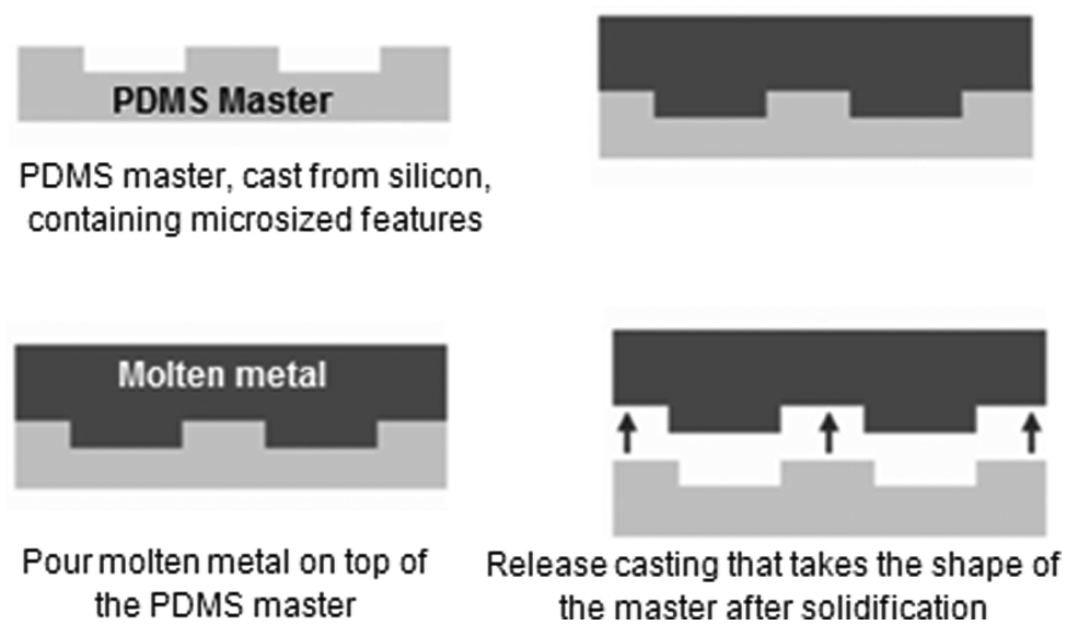
Schematic of microcasting process for metal using silicone master.
Theoretical and experimental investigations
Due to decrease in the dimensions of casted part, some issues such as complete mold filling, suitable operational pressure and other parameters become important in microcasting technique. The casting parameters (casting material, investment’s preheating temperature and filling pressure) govern achievable grain size and resulting mechanical properties of microcast parts. 92 The castability of any material is determined by its properties such as flowability and form filling ability, shrinkage, segregation, porosity, hot crack susceptibility, surface quality, achievable grain size and resulting mechanical properties of the microcast parts. The form filling ability and flowability of the melt are influenced by viscosity of melt, wetting behavior of form, reaction with mold and atmosphere and, of course, solidification behavior. 92 The research and development concerning microcasting was started with precious alloys, such as gold alloy, Sn-36Pb-2Ag alloys due to relatively low melting temperature and good fluidity. Previous investigations led to the choice of the particle hardened gold base alloy Stabilor-G®, which is used in the dental applications. To expand the industrial applications domain of microcasting, aluminum base alloys can be potential candidates (e.g. Zn–4% Al alloys). 85 Another typical material can be bronze that shows good slip properties. A high form filling ability and a good flowability are guaranteed for these materials to be used in jewelry, dental casting, handcraft arts made of bronze and in scenario where high-strength materials (e.g. CoCrMo alloys) are required. Steels are not widely used in microcasting because of their oxidation and corrosion sensitivity. 92 Another aspect is fast solidification in small structures due to very high cooling rate. This hinders form filling much more than macrostructures. Furthermore, the occurrence of turbulent flow needs to be taken into account due to higher surface-to-volume ratio in microchannels and distinct influence of surface roughness.
In microcasting, length scale is very small, so issues such as mold filling, progress of solidification, shrinkage, segregation and surface roughness (finish), which were of macroscale in macrocasting, now should be treated as meso- and microscale phenomena. It is discussed in Xiangdong et al. 99 that for fluid flow in cavities larger than 10 times of fluid molecular diameter, the continuum hypothesis is still valid and Navier–Stokes equation can be used to analyze the flow. The channels’ dimension in microcasting is of the order of hundreds of micrometers, which are sufficiently far from fluid molecular diameter. Thus, continuum hypothesis and Navier–Stokes equation along with some suitable solidification models should still be valid for modeling microcasting fluid flow, filling behavior, solidification, as-cast grain morphology and nucleation and growth kinetics of grains.
Modeling and simulations can be used to overcome challenges in microcasting process and to optimize the process parameters. Such computational method based on deterministic solidification, heat transfer and fluid flow models100,101 can provide predictive capability and deeper insights of filling behavior (role of viscosity, capillary, surface tension, mold roughness and preheat temperature, centrifugal force and applied pressure), progress of solidification (interface location, solidification time and local cooling rate), segregation behavior and casting defects.
In order to obtain more insights and deeper understanding of various transport phenomena taking place during microcasting process, the data for validation of numerical models, experimental data for local temperature and composition measurements and defects analysis in microcast parts are also needed.
Applications
Several material properties such as drag, friction, adhesion and hydrophobia can be adapted in components manufactured by microcasting. 94 Possible applications of microcastings include cast parts where a reduced wettability or a self-cleaning effect is desired. Cast parts that become rapidly dirty, such as wheel rims or under body of cars and motorbikes, represent very interesting applications for microstructured surfaces, especially in terms of corrosion protection. Another field is industrial facilities such as chemical or power plants with complex piping and pumping systems, which are very difficult to maintain and clean. Furthermore, microholes can be used for tribological applications, for example, reservoirs for lubricant films in cylinder–piston pairings or bearing blocks in engines. 94 Several other applications of microcast components are possible, such as small-sized instruments for surgery, dental devices, biotechnology, jewelry and dental castings.
Remarks
As discussed above, various investigations have demonstrated that microcasting is a potential fabrication method for metal parts in microdimensions. Since this technique is at its developmental stage, much more work is needed to make this technology suitable for use in industries. Future research on microcasting can focus on the following:
Physical understanding of the mechanism of formation of final metallographic structure associated with high cooling rate in microcasting process. It is an interesting design problem when grain sizes in microcasting are close to the length scale of the device’s features. For faster transition of academic research to an industry, better understanding of various microcasting techniques clearly marking their merits, possible applications and exploring various microcast materials is needed.
Another interesting area of research is development of a microchill-mold technique using permanent molds instead of lost molds to obtain a higher level of automation. 92
Development of roll-to-roll processes in order to produce microstructured surfaces with low cost and high throughput. Here, molten metal could enter a cold polymer roller, and the roller could press the metal into its microstructures, producing solidified microstructured metal in a continuous sheet form. 97
Exploring casting of real 3D microparts with inner microfeatures and undercuts. 92
Micro Joining
The fabrication of various man-made product manufacturing and assembly providing mechanical support and integration, electrical connection, optical coupling, environmental protection and so on cannot be realized at all scales (macro, micro and nano) without the aid of joining processes (welding, soldering and brazing). The continuing miniaturization of engineered devices and systems, coupled with ever-growing demands for cost reduction, enhanced performance and reliability and so on, brings new challenges to the technology of joining. While defining the regime, the widely accepted definition of micro joining (MJ) is the process dealing with at least a part having characteristic dimension of smaller than a few hundred micrometers but larger than hundreds of nanometers. 102 MJ processes are not new to the industries, their origin traces back to the 1950s. A capacitor discharge machine was introduced then for resistance welding of orthodontic appliances, and this development was later adopted in the aerospace industry in the 1960s. 103 Thermo-compression wire bonding, a variant of hot pressure welding, was developed by Bell Laboratories in 1957 104 and later it evolved into ultrasonic wire bonding in 1960s and thermo-sonic wire bonding, a combination of thermo-compression and ultrasonic wire bonding, in 1970. 105 Thus, the MJ has been known in manufacturing for more than five decades in microelectronics, medical, aerospace and defense industries; the process has been continuously facing challenges primarily due to ever advancing miniaturization. The novel MJ processes have been playing a deterministic role in packaging and interconnecting in MEMS, where individual electrical, mechanical, fluidic and optical components need to be connected and coupled to the macroscopic external environment. 106 The joining technologies in MEMS are challenging as they are widely used in sensor technology. In such applications, they need to be protected from mechanical damage and corrosion at one end, while they must be exposed as intimately as possible to the environment to obtain true, undistorted physical and chemical values on the other hand. 106 Hence, MJ technology will continue to play a pivotal role in industrial acceptance of the age of miniaturization.
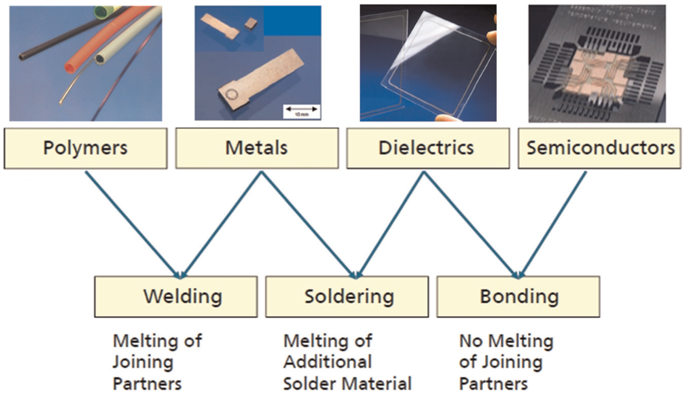
Deriving from the first principle, two ideal solid surfaces, for example, both perfectly clean and atomically flat, will join together if brought into intimate contact, because they will be drawn together spontaneously by interatomic forces. 102 The driving force for this joining is the reduction of Gibbs free energy of the system by eliminating, reducing or replacing high-energy free surfaces by low-energy interfaces. This basic principle is behind all the joining processes at all the scales. But most engineering surfaces are characterized as rough and contaminated with oxides and so on requiring some form of energy, usually heat and/or pressure, to be applied to overcome these surface impediments to make a joint. Based on the physical state of the parts, the joining processes are classified into four basic types—solid-state bonding, soldering/brazing, fusion welding and adhesive bonding. This classification was primarily developed for metals and latter it was widely accepted for all types of joining processes including MJ processes. Based on this criterion, the classification of MJ processes is presented in Figure 14. Solid-state bonding is mainly achieved by pressure where no melting occurs, but solid-state diffusion assists/promotes the joint formation. Fusion welds and brazed/soldered joints are achieved by melting and solidification of molten metal. There is localized melting of base metals in fusion welding, while melting of only filler metal occurs in brazing and soldering with melting temperature of filler metal above 450 °C and below 450 °C, respectively. In adhesive bonding, organic adhesives are used to join the parts together. Adhesive bonding, soldering and brazing can be easily applied to dissimilar materials if the adhesives, solders or brazes are compatible with both the materials that are involved in joining process. Interlayers may be needed in solid-state bonding of dissimilar material parts. Among all the processes described above, the processes using high-energy density beams (electron or laser) to achieve local melting of the substrate or filler metal have numerous advantages. They can be focused down to a few micrometers facilitating high local temperature and very low heat input into the workpiece, and they are highly flexible. Ease of manipulation and possibility of processing in open atmospheric conditions give laser beam processing an extra edge over electron beam processing. Hence, laser MJ is evolving as a prospective smaller scale manufacturing process in the growing technological field like MEMS and biomedical applications.
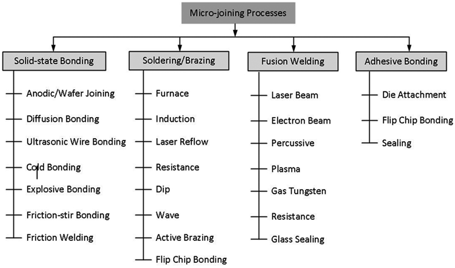
Classification of microjoining processes.
A number of research articles and patents on the design of apparatus and methodology in this area show the signature of developments in the field. The latest developments in the field of laser technology brought new opportunities for laser to join a wide variety of materials used in microsystems. However, the feasibility of MJ still mainly depends on pulse modulation strategy and wavelength for selective range of laser power and laser irradiation intensity. The classification of laser MJ processes is presented in Figure 15. The microwelding process involves melting of two metals during joining process, while the laser microsoldering and laser microbrazing processes involve the addition of soldering and brazing material, respectively, during the joining process. The following section deals with various aspects of microscale joining process in the perspective of practical applications. This review presents not only the experimental investigations and applications but also it discusses the future research trends and potential applications of MJ.
Classification of laser microjoining processes.
Types of lasers for Micro Joining
The term MJ commonly refers to the process where at least one dimension of the part being processed is less than 100 μm. The difference between traditional and MJ is that the latter is performed at extremely low power in combination with fine control of the power source. 107 Neodymium-doped yttrium aluminum garnet (Nd:YAG) and CO2 lasers are commonly used in the industries. Nd:YAG is a solid-state laser where lasing action is extracted from an Nd:YAG rod. This laser is available in both pulsed and continuous wave (CW) modes. But Nd:YAG in pulsed mode is preferred over the CW Nd:YAG because the making of CW laser is not straightforward as compared to that of the pulsed mode. The CO2 laser is a gas laser and CW mode of operation has been the preferred mode of operation. Fiber and diode lasers are getting popularity in the field of material processing. Fiber lasers produce beams of very high quality and thus can be focused down to a very small size spot. Fiber lasers are pumped with laser diodes and offer higher efficiency than other lasers used for similar applications, like Nd:YAG laser and CO2 laser. In diode lasers, a bank of laser diodes is directly used for producing laser beam. 108 Disk lasers are also making inroads with their high beam quality and CW operation. If we compare the performance of these lasers for laser–material processing applications, Nd:YAG lasers have a wavelength of 1064 nm, which is exactly 10 times smaller than CO2 lasers and preferred choice for producing very fine spot. Due to absorption of wavelength, Nd:YAG lasers work efficiently on metals (absorption of Nd:YAG laser: 10%−40% and CO2 laser: 5%−10% 109 ), while the processing of organic materials such as wood, acrylic, plastics and fabrics is preferably done with CO2 lasers. The wavelength of fiber laser is close to Nd:YAG laser and its high-quality beam due to its inherent generation methodology makes it promising. Diode lasers are characterized by their ability to be focused into very fine spots on account of their small wavelength of 800–976 nm. They can be used very efficiently for processing of plastic materials. A recent innovation of 532 nm green Nd:YAG-pulsed laser has provided an order-of-magnitude increase in its absorption over the 1064 nm wavelength laser and expanded use of the lasers in microwelding of highly thermal conductive materials. Green laser beam in the visible spectrum is better absorbed by highly reflective materials that cannot be done with a traditional 1064 nm YAG laser. All the lasers in near infrared (IR) and visible range, that is, Nd:YAG, diode and fiber lasers, can be delivered through optical fibers, and therefore, these lasers offer ease of processing. As no optical fiber is available for CO2 lasers, the reflective optics is used to deliver the laser beam at the processing point. 109 Thus, advantages and limitations of these lasers are application specific. In MJ, the fiber or direct diode laser is preferred for precise focus diameter and controlling of energy transfer. However, the Nd:YAG dominates in industries due to long history and flexibility of pulse shaping during joining of highly thermally conductive materials or dissimilar materials.
Laser Micro Joining system
The general configuration of laser MJ system is similar to the conventional laser processing system. A laser generated in the system is either transmitted through optical fiber or reflective optics and refractive focusing optics to the processing point. The focusing refractive optics is a preferred choice due to its inherent advantages of focusing the laser beam to a smaller diameter spot. Figure 16 presents a general configuration of laser MJ system. A near-diffraction limited laser and good beam delivery system delivers a laser beam of diameter lesser than 100 μm at the processing point. The components to be joined are lapped or butted together and scanned with a focused beam along the joint with a certain speed. The energy is absorbed by the component and its temperature goes up. The temperature crosses the melting point of the material and it is overheated a bit (may be 100 °C–200 °C above the melting point). The CW laser continues with molten pool and joins the component. In both the cases, the processing parameters are selected in such a way that there is a precise control on heat-affected zone (HAZ).
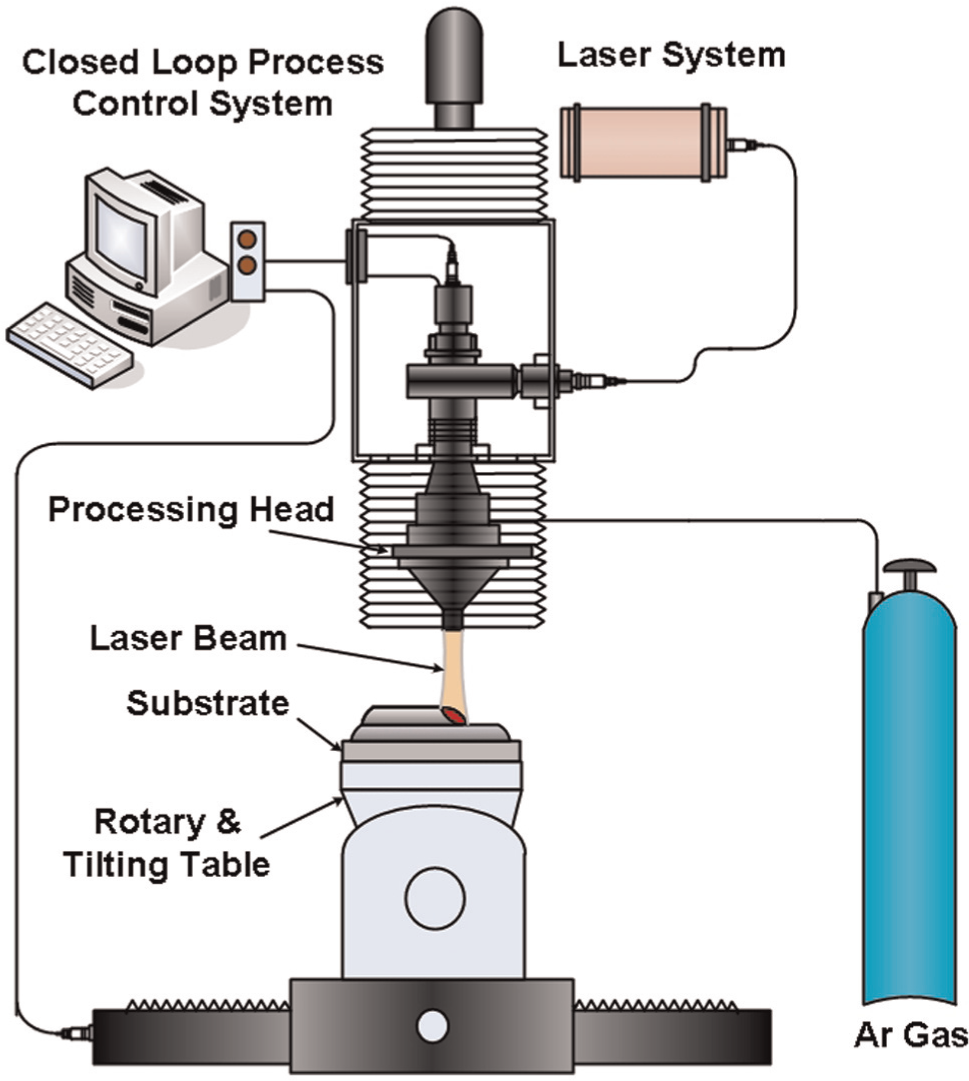
General configuration of a laser microjoining system.
Laser transmission welding is another configuration used by researchers and different industries such as automotive, electronic and biomedical engineering. Unlike standard welding where energy is applied at the surface of the materials, transmission welding aims to apply the energy in between two plastic pieces at their interface. The upper layer needs to be transparent to laser wavelengths in the IR and near-IR spectrum. Typical laser wavelengths are of 808 or 980 nm. Once the laser beam passes through the upper layer, it still needs to be converted into thermal energy. This happens at the interface of the two joining parts. The lower part needs to have the ability to absorb the light energy to create heat. Most thermoplastics naturally transmit IR laser radiation so absorptive properties are realized by adding soot or pigmentation. The most common and best absorbing additive is carbon black doped at a rate of about 0.5%. 110
The latest development in the field of polymer welding using high brilliance laser source together with advanced irradiation strategies based on the local and temporal modulation of the laser beam is TWIST 111 (Figure 17). For this process, a dynamic periodic beam deflection is applied to control the fusion and solidification processes where high dynamic beam oscillations are overlapped to the normal welding direction along the welding contour. High dynamic oscillations prevent thermal damage; hence, a more homogeneous energy input across the weld seam width can be achieved. The idea of CW welding for microparts using temporal shape of the laser pulse led to recent development of SHADOW technique. It realizes extended weld seams with a pulsed laser using single pulse and sweeping the laser beam over the surface during the pulse. 112 This method produces smooth continuous surface as compared to pulse shaping methods. The application of SHADOW technique is mainly found in joining of metals and alloys in repairing of watch components, that is, joining between stainless steel and highly conductive copper.
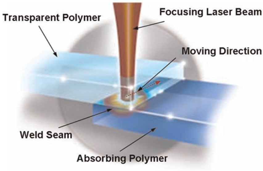
General configuration of laser transmission welding.
Grewell et al. 113 devised diffractive optics to reshape lasers for welding of plastics. Using inverse Fourier transform, diffractive lenses are designed and fabricated to shape the beam into predetermined patterns. This method can obviously be applicable to both modes of laser welding of plastics, that is, surface heating and through transmission IR welding. The welding technique uses diffractive optics for laser beam shaping using mask, not the concept of scanning. Schmitt et al. 114 developed a miniaturized scanner-based laser microwelding system by integrating a beam deflection option for welding of metal as well as plastic materials. Highly dynamic oscillation techniques lead to the stabilization of welding process of difficult-to-weld materials with an increased process velocity. The process requirements are suitable beam deflection system and design of a miniaturized laser processing optics. However, the selection and integration of highly dynamic scanner system and process enable further improvements in laser beam microwelding.
Thus, a number of methodologies are being developed with a special emphasis on precise control of laser pulse shaping for improved laser MJ. These developments also address application specific issues and prove their potential for various futuristic uses.
Process parameters
Since the laser MJ involves a number of systems and many parameters, the results of MJ depend on them. Figure 18 summarizes the process parameters that influence the outcome of laser MJ process. These parameters can be divided into four major categories: laser, optics, system specific and material specific.
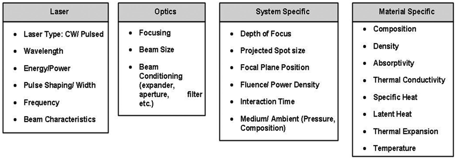
Relevant processing parameters for laser microjoining.
Among laser and optics parameters, many parameters such as mode, wavelength, type of laser operation (CW/pulsed) and focal length are fixed for a selected laser and optics. The material-specific parameters are crucial and primarily govern the quality of microjoint. These parameters have some interdependence, and hence, understanding of independent effect is important for process developing engineers. The spot diameter obtained in lens focus (d 0) can be obtained as

where ƒ is the lens focal distance (mm); D is the lens opening (mm) and λ is the wavelength of emitted radiation (μm). Maximum power density (Wp ) in focused beam is given by
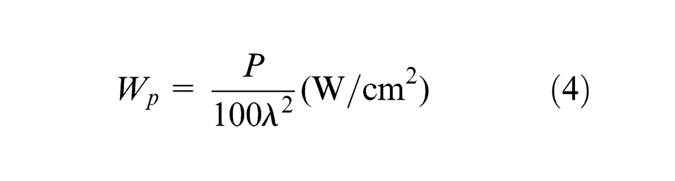
where P represents the power emitted by laser radiation (W).
The laser power determines the penetration depth; laser power density/intensity is dependent on cross section of the laser beam. Laser energy determines the volume of molten material and can be calculated by the product of power and laser–material interaction time or the product of laser power and pulse duration. The recent advances in electronics and computing offered special pulse shaping capabilities to lasers. Pulse shaping is a technique that is used to temporarily distribute energy within a single laser pulse that provides the user an added degree of control over the heat delivered to the laser–material interaction zone. The modulation of pulse in time domain enables to endorse keyhole or conduction mode welding, optimization of penetration depth and welding of highly reflective materials in conventional pulsed laser welding process. 115 In conduction mode laser welding, typically a low peak power and a long pulse time are used, whereas keyhole mode welding is characterized by high peak power at a short pulse time. In full-depth penetration, the pulse shape has typically a low peak power over a certain time and the peak power is raised suddenly to melt the second material, and finally the power is reduced gradually to stable the melt and to cool down. A high peak power is used to melt highly reflective material and a rapid reduction in peak power is followed to avoid overheat. Therefore, the melt grows under low peak power and long pulse time. 116 A typical pulse shape for crack-sensitive materials has an upslope at the beginning of the pulse to prevent thermal shock and a down slope at the end of the pulse to have a controlled cooling down period. By controlling the cooling down phase, the thermal shrinkage stresses are reduced 117 for crack-sensitive materials. It is thus obvious that pulse shaping provides added capacity to overcome some intrinsic problems during joining of materials. Hugger et al. 118 successfully conducted microwelding of aluminum and copper using pulsed Nd:YAG laser where surface roughness and distortion are reduced by pulse shaping. There is a significant development in optical waveform synthesis or pulse shaping of ultra-short laser in picosecond and femtosecond range. 119 However, production of state-of-the-art pulse shape at micro–nano–pico–femto-second level is a challenging task, and the influence of pulse shaping in ultra-short pulse laser welding is an open area of research for precision joining of materials at microscale.
Applications
The recent advances in laser MJ have opened new avenues in electrical contacts of automotive and consumer electronics, mechanical contacts in micromechanics, electrical contacts and seals in medical engineering. The MJ is used in overlap and butt joint configurations of various materials including highly reflective materials with controlled heat input achieving desired strength especially for wire bonding. This research trend shows that a direct diode laser without an optical fiber and low-power fiber lasers are promising alternatives of Nd:YAG laser in MJ process. 120 The CW single-mode fiber laser is more suitable for stainless steel and titanium alloys up to 1-mm-thick foil. However, to weld reflective materials like aluminum and copper base alloys and dissimilar materials, pulsed Nd:YAG laser is a better choice. The welding of thin foil of stainless steel using direct diode laser at high laser scanning speed needs low power density than CO2 or Nd:YAG laser. 121 The recent advances in fiber lasers have brought superior pulse-to-pulse energy stability. 122 Recent fiber laser is characterized by high peak power, high repetition rate with single-mode beam quality and low pulse energy, whereas Nd:YAG laser is characterized by low peak power, long high-energy pulses but poorer beam quality. One of the major challenges in microwelding process is to join dissimilar materials. The primary issue for dissimilar materials welding is the possibility of mismatch in the physical properties and poor metallurgical affinity between two materials that lead to the formation of crack and brittle intermetallic phases. 123 This can be overcome by adding a third material as filler that helps in reducing brittle intermetallic phase. Laser MJ has many attractive applications in joining nonmetallic materials such as glass, silicon and plastics. 124 These nonmetallic materials are generally joined by transmission welding. The wavelength of laser source is chosen in such a manner that the substrate material acts as transparent and ultra-short pulse (femtosecond) laser serves this purpose. Microwelding of glass and silicon has high potential of applications in electronics industries since they are semiconductor materials. However, an intermediate layer of the order of micrometer is used for laser transmission welding where the layer absorbs the laser irradiation. Sometimes, a shadow mask of reflective material is used to control local heating in the desired area in the case of nanosecond-pulsed Nd:YAG laser. It is noteworthy that Nd:YAG laser is not so precise as ultra-short pulse laser, but it is possible to reshape the pulse according to the application. In joining of plastic components, near-IR laser radiation is generally used by transmission welding. The welding between polyethylene (PE) film and black PE sheets are performed using diffractive optics to reshape laser beams of YAG laser. 113
Recently, the transmission welding of biocompatible materials such as polyimide (PI) and titanium (Ti) is observed in medical implant devices and neural implant devices. 110 Fiber laser or near-IR diode laser is a choice where formation of the joint is a result of the creation of strong chemical bonds between Ti and certain polymeric functional groups. An interesting application of microwelding between copper ball and borosilicate glass using a nanosecond pulse Nd:YAG laser is observed in measurement hardware, solar batteries and touch panels. 125 In one of the recent studies, 100 fs laser welding was carried out on an 800-nm Ti foil. Sapphire laser system with a pulse energy of 250 μJ/pulse and repetition rate of 1 kHz was used. 126 Au nanoparticles were synthesized by citrate reduction of HAuCl4. Welding was done in liquid by focusing the laser into a quartz cell or in solid by depositing Au nanoparticles onto a transmission electron microscopy (TEM) Cu grid.
Remarks
There is enormous scope for the applications of this process in new products as the miniaturization of the products is appended every day. The applications area of MJ includes MEMS, medical devices, packaging technology, lightweight automotive structures and sensor industries where highly integral products are joined with accuracies of few microns. The feasibility of the process for new materials, more dissimilar material joining and various geometric configuration welding are future prospects for this joining process. The real challenge lies in welding of dissimilar materials due to wide difference in material properties and the nature of contact surface. Moreover, the success of the microjoint depends on the accurate design, selection and control of input laser parameters avoiding insufficient joint strength or damage material. The geometric precision, cost of equipment and associated economics are future challenges for the application of laser MJ technology in mass production.
Conclusion
Form the above review of microforming, microcasting and MJ processes, the following conclusions can be made:
Micromanufacturing in general and mass content micromanufacturing processes (microforming, microcasting and microwelding) in particular have extensive applications in coming future due to inherent advantages of miniaturization.
Microforming, microcasting and microwelding need extensive research work with reference to the process development, data bank generation, theoretical analysis, simulation and modeling of the processes.
An important area of research where attention of the researchers is required is the new micromanufacturing processes and setup development. Multi-objective parametric optimization of these processes will yield the desired results in terms of dimensional accuracy, surface roughness and tolerances.
Footnotes
Declaration of conflicting interests
The authors declare that there is no conflict of interest.
Funding
This research received no specific grant from any funding agency in the public, commercial, or not-for-profit sectors.