
Abstract
The objective of this study is to design and evaluate soft abrasive wheels for silicon wafer grinding. In this study, CeO2, SiO2, Fe2O3 and MgO soft abrasives are used in the design of soft abrasive grinding wheels. The soft abrasive grinding wheels are then used to grind silicon wafers and compared with diamond wheel grinding and chemomechanical polishing. This study demonstrates that the newly designed soft abrasive grinding wheels are generally superior to diamond wheel grinding or chemomechanical polishing in terms of wafer surface/subsurface quality, wheel dressability, grinding ratio and material removal rate. This study further identifies the MgO soft abrasive grinding wheel as the best of the four soft abrasive grinding wheels. Discussion is provided to explore material removal mechanisms, wheel dressing characteristics and wafer surface finish and quality of the newly designed soft abrasive grinding wheels.
Introduction
Monocrystalline silicon is widely used as a substrate material in the integrated circuit (IC) manufacturing field. The surface layer quality of a finished wafer directly affects the performance, the manufacturing yield and the lifetime of the IC device. With the development of the IC technology, the demand for better surface layer quality of silicon wafers is getting higher.
Ultraprecision grinding is one of the important methods in machining of silicon wafers and in back-thinning of the completed device wafers.1–3 The greatest challenge in the traditional grinding of a silicon wafer with a diamond wheel is the suppression of surface layer damage.4–7 Once formed, the surface layer damage needs to be removed by the subsequent processes, which adds tremendous cost and time to the IC manufacturing processes. Therefore, it has been a research focus on how to reduce or even eliminate the surface layer damage induced during the grinding process.
To suppress the formation of surface layer damage in a grinding process, diamond wheels of fine grain sizes are often used. As the grain size of a diamond grinding wheel is sufficiently small, one can effectively reduce surface layer damage and surface roughness. However, if the grain size is reduced to a certain critical value, it is difficult for the grinding wheel to maintain self-dressing ability. 8 (Self-dressing ability refers to the ability of a wheel to release worn grains and expose new grains without any external assistance.) In order to maintain constant sharpness of the diamond wheels of fine and even ultrafine grains, electrolytic in-process dressing (ELID) has been introduced to the wafer grinding.9–16 Although ELID can help the grinding wheel maintain its sharpness, it also faces several technological barriers that have to be overcome before it becomes a viable manufacturing process. For example, (a) the ELID grinding has difficulty achieving the super-flatness that can be routinely achieved in a conventional wafer grinding process; 16 (b) wheel wear must be compensated in time in order to obtain high-dimensional accuracy as the grinding wheel is automatically dressed during the ELID grinding process and (c) the ELID grinding removes diamond abrasives prematurely, resulting in the waste of the abrasives and therefore a shorter wheel life. 17 Furthermore, the electrolytic fluid and the metal bond wheel used in the ELID grinding may contaminate the device wafers, leading to poor device performance. 16
Nevertheless, the surface layer quality of a ground wafer is improved by decreasing the individual grain depth of cut (DOC) of a diamond wheel. If the individual grain DOC is less than the critical cutting depth of the monocrystalline silicon, the ductile mode grinding is expected, which allows to have better surface finish and less subsurface damage. 18 However, plastic strains are generated in the wafer surface layer during the ductile mode grinding process and lead to subsurface damage in the form of dislocation and amorphization. 19
To minimize damage formation in grinding of silicon wafers, a fixed abrasive machining technique named chemomechanical grinding (CMG) has been recently developed.20,21 In the CMG technique, soft abrasives are generally used in the design of a grinding wheel. It has been demonstrated that the CMG process with soft abrasive grinding wheel (SAGW) can significantly reduce or even eliminate the surface layer damage by decreasing the abrasive hardness of the grinding wheel and introducing proper chemical reactions to the wafer grinding. The CMG process has the advantages of both the conventional wafer grinding and the chemomechanical polishing (CMP). It can generate superior surface quality comparable to that of CMP while still maintaining high-dimensional accuracy. CMG is considered to be a promising wafer processing method. Ultrasmooth and damage-free silicon wafers could be achieved with the CMG process.20–27 Although CMG is found to be promising for wafer grinding, it still has problems that need to be solved. The problems include unstable grinding performance, low material removal rate (MRR), grinding burn, wafer surface scratches and so on.24,25
This study builds upon the previous research on SAGW design. It optimizes design and formulation of the SAGW. This study further investigates the grinding performance of the newly designed SAGWs of different soft abrasives in terms of wafer surface roughness, surface/subsurface damage, wheel dressing interval, spindle motor current, grinding ratio and MRR.
Design of SAGW
The CMG process is able to achieve supersmooth and low-damage wafer surface by utilizing the mechanical friction of soft abrasives and chemical reaction between the abrasives, additives and silicon. A typical CMG process has four stages and is illustrated in Figure 1. In stage I, the SAGW and the wafer surface come into mechanical contact. In stage II, the soft abrasives are exposed and the additives are continuously released onto the wafer surface through the SAGW wear and self-dressing effect. In stage III, complex chemical reactions occur between abrasives, additives and silicon when the mechanical contact between SAGW abrasives and wafer surface provides sufficient heat and pressure. At the contact interface between the abrasive and wafer surface, a loose and soft reaction layer is generated. In stage IV, the generated loose and soft reaction layer on the wafer surface is easily removed by the mechanical friction between SAGW and wafer surface. No significant surface layer damage is induced by the SAGW because the abrasive hardness of the SAGW is lower than that of the monocrystalline silicon. As a result, fresh and damage-free wafer surface is continuously generated as the four stages repeat in the CMG process. In the whole CMG process, stages I and IV can be considered as mechanical action dominant while stages II and III as chemical action dominant. Therefore, material removal mechanism in the CMG process is considered a combination of chemical and mechanical actions.
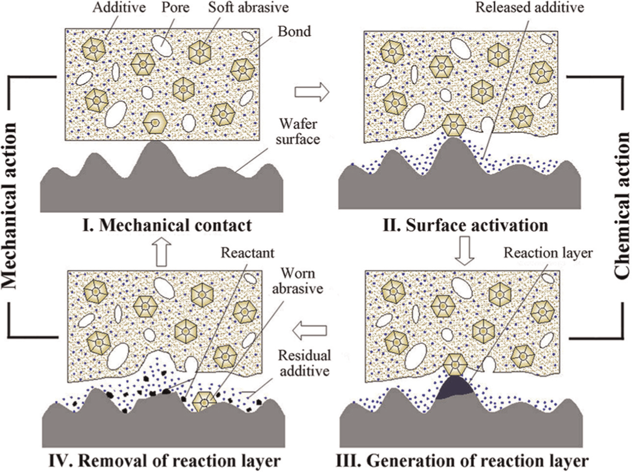
Four stages of material removal in the CMG process of silicon wafers with SAGW.
Based on the material removal mechanism of CMG above mentioned, the SAGW needs to meet the following requirements in order to achieve supersmooth, damage-free wafer surface: (1) the abrasives with ultrafine grain size, (2) the abrasives softer than silicon for scratch-free wafer surface, (3) the abrasives chemically reactive with silicon in the grinding process and (4) the additives to the SAGW chemically reactive with silicon or promoting the chemical reaction between the abrasives and silicon.
Ceria (CeO2) was mainly chosen as an abrasive of the SAGW and has exhibited good performance in the silicon ultraprecision grinding.20–26 Chemical reaction between CeO2 abrasives and silicon during the grinding process was also studied.26,27 However, few researchers investigated the grinding performance of SAGWs with different soft abrasives. In this study, four soft abrasives of 3000 are used in the SAGWs for silicon ultraprecision grinding and are compared in terms of their grinding performance. Figure 2 shows the Mohs’ hardness of monocrystalline silicon and some commonly used abrasives. It can be seen that the hardness of ceria (CeO2), silica (SiO2), iron oxide (Fe2O3) and magnesia (MgO) are all lower than or close to silicon. Moreover, CeO2, SiO2, Fe2O3 and MgO can also react with silicon under certain conditions and can be used as abrasives of SAGWs for silicon wafer grinding.
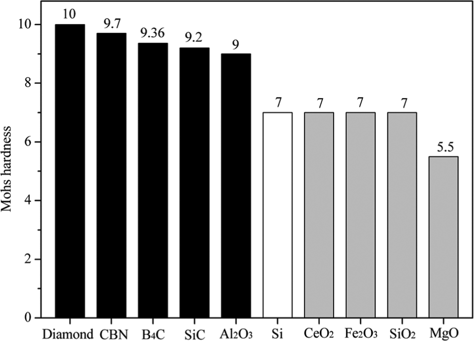
Mohs’ hardness of monocrystalline silicon and some abrasives.
Different additives including Na2CO3 and CaO were employed to enhance the chemical effect or to accelerate the chemical reaction between the abrasives and silicon. Compared to the vitrified and metal bond grinding wheels, the resin bond grinding wheel has the advantages of easy preparation and dressing, good elasticity, better wafer finish and so on. Resin bond was used as the bonding material of the SAGWs in this study. In order to improve self-dressing ability of the SAGWs and reduce grinding force during the grinding process, 7% volume porosity was provided to the SAGWs during the fabrication process. The detailed compositions and specifications are listed in Table 1. Figure 3 shows one of the developed SAGWs. The SAGW consisted of 29 segments. Each segment was 7.5 mm thick and 7 mm height. The segments were glued on the grooves, distributing along the rim of a stainless steel wheel frame of 354 mm in diameter.
Compositions and specifications of SAGWs (vol.%).
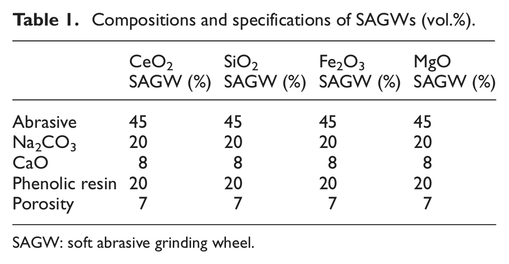
SAGW: soft abrasive grinding wheel.
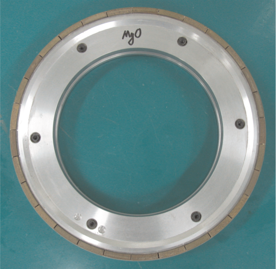
Image of MgO SAGW.
Grinding experiments of silicon wafer
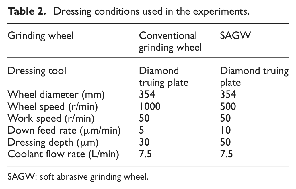
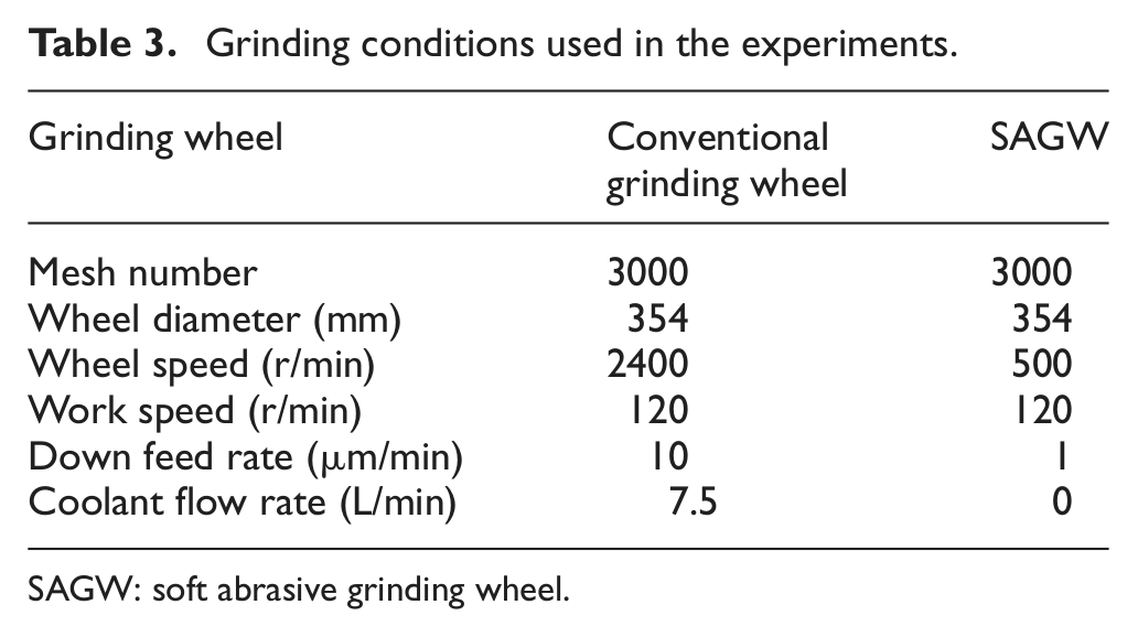
Grinding experiments were performed on a wafer grinder (VG401 MK II, Okamoto Corp., Japan) on which the wafer is ground according to the principle of the wafer rotation grinding. An online measurement device with 1 µm accuracy was used to monitor the change in the wafer thickness and give a feedback to the grinding control system. Figure 4 shows the grinding arrangement with the newly designed grinding wheels. For comparison purposes, a conventional resin bond diamond wheel of 3000 (Asahi, Japan) was also used in the grinding experiments. After being mounted to the wafer grinder, the SAGWs and conventional diamond wheel were dressed using an electroplated diamond truing plate with mesh number of 320; the dressing conditions were shown in Table 2. Because the bonds of SAGWs and conventional diamond wheel were all resin bond, the in-process dressing (such as ELID) was not needed during the wafer grinding. (100) Silicon wafers of 150 mm diameter were preground with a 2000 diamond wheel as the workpiece wafers. Deionized water was used as the grinding coolant. Table 3 provides grinding conditions for the SAGW grinding and diamond wheel grinding (DWG).
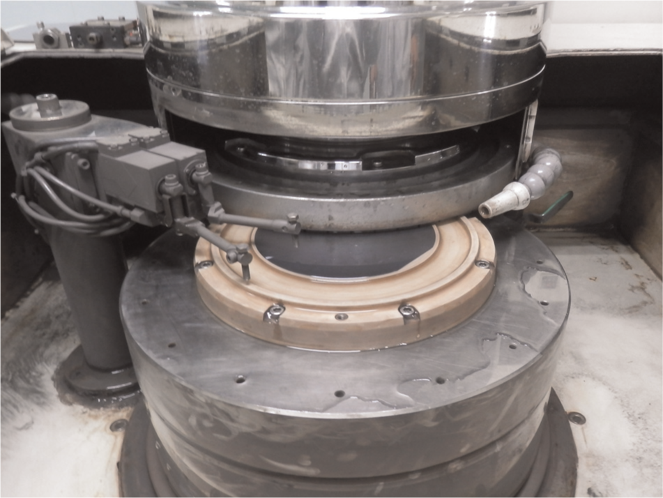
VG401 MK II wafer grinder.
Dressing conditions used in the experiments.
SAGW: soft abrasive grinding wheel.
Grinding conditions used in the experiments.
SAGW: soft abrasive grinding wheel.
After each test, the ground wafer was observed with a scanning electron microscope (SEM; Quanta 200; FEI Corp., USA). Surface roughness and topography were measured with an atomic force microscope (AFM; XE-200; Park Systems Corp., Korea). The ground wafer was also observed by the cross-sectioning technique combined with a transmission electron microscope (TEM; Tecnai G220 S-Twin; FEI Corp.). A Hall-effect sensor was incorporated into the grinder to monitor the spindle motor current so as to real-time display the grinding force in the wafer grinding process. Grinding ratio (the volume of the wafer material removed vs the volume of the wheel wear) was calculated to characterize the wear resistance of a grinding wheel. To assess the grinding performance of the SAGWs, MRR was used to evaluate the volume of material removed by the grinding wheel per unit time.
Experiment results and discussion
Characteristics of machined wafer surfaces
Following the fabrication process, all the four SAGWs were balanced and tested for mechanical strength information. The four SAGWs were then used in the grinding experiments on silicon wafers. For comparison purposes, the grinding results were compared with that obtained using the conventional diamond wheel and the CMP process. Figure 5 shows the silicon wafers machined by the conventional diamond wheel, the SAGWs and CMP. Neither edge chipping nor breakage was observed in any of these wafers. Although all the wafers exhibited clean mirror surfaces, a radical swirl pattern of light reflection was observed from the wafer surface ground by the conventional diamond wheel, depicting an inferior surface finish. To confirm surface finish of these wafers in a more deterministic manner, SEM observations were conducted on these wafers. It can be seen that the wafer surface ground by the conventional diamond wheel obviously had grinding marks, but the surfaces machined by the SAGWs and CMP were all defect free (no scratches, pits, microcracks and so on).
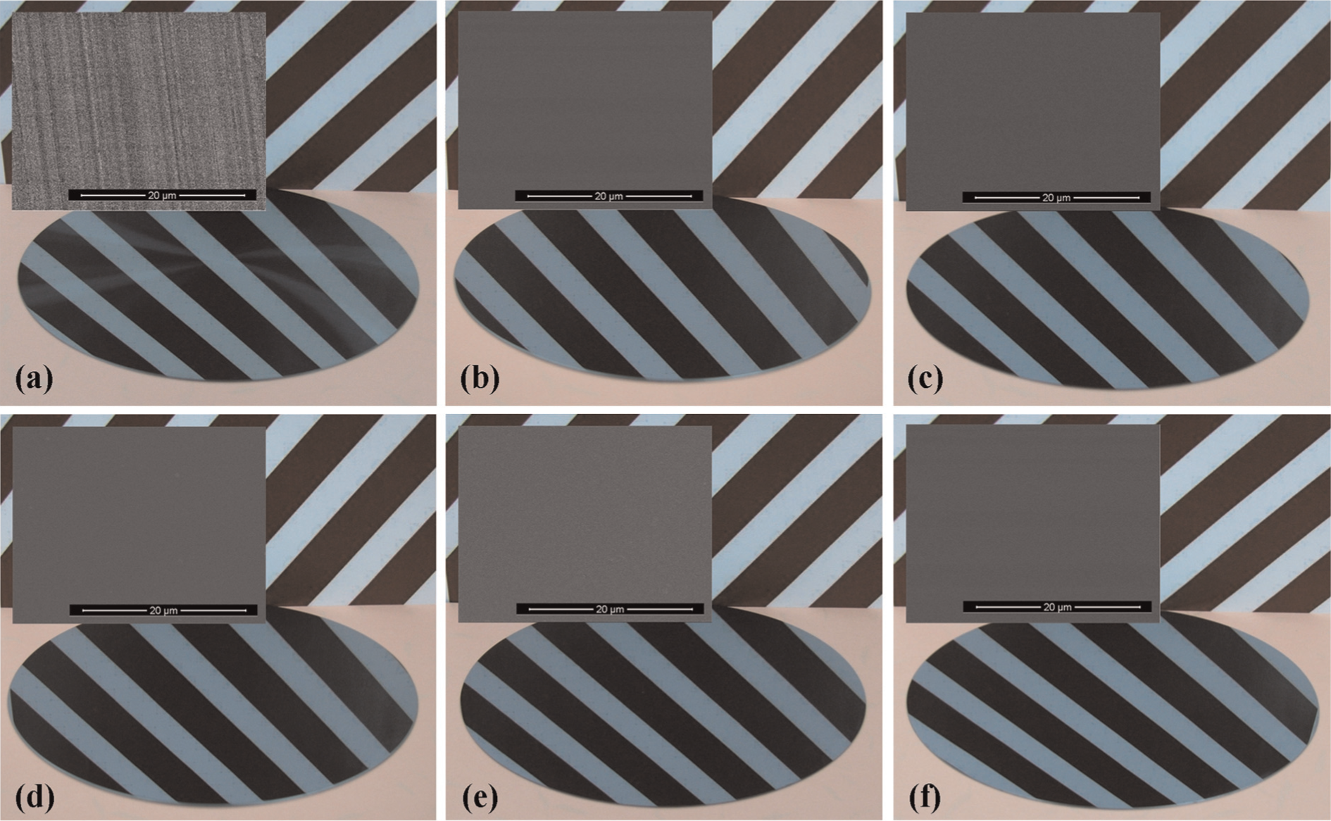
Silicon wafer machined by (a) conventional diamond wheel, (b) CeO2 SAGW, (c) MgO SAGW, (d) SiO2 SAGW, (e) Fe2O3 SAGW and (f) CMP.
Figures 6 and 7 show the surface roughness and the topography of silicon wafers ground with the conventional diamond wheel, the SAGWs and CMP. Surface roughness Ra of the silicon wafer ground by the four SAGWs was all less than 2 nm and was far better than that with the conventional diamond wheel. Specifically, the MgO SAGW ground wafer had its surface roughness Ra comparable to that by CMP. It is interesting to note from Figure 7 that the surface topographies of silicon wafers machined by the SAGWs were all similar to that by the conventional diamond wheel but evidently different from that of the CMP wafer. Grinding marks were observable on the wafer surface ground by the SAGWs, although they had much smaller depth than that by the conventional diamond wheel.
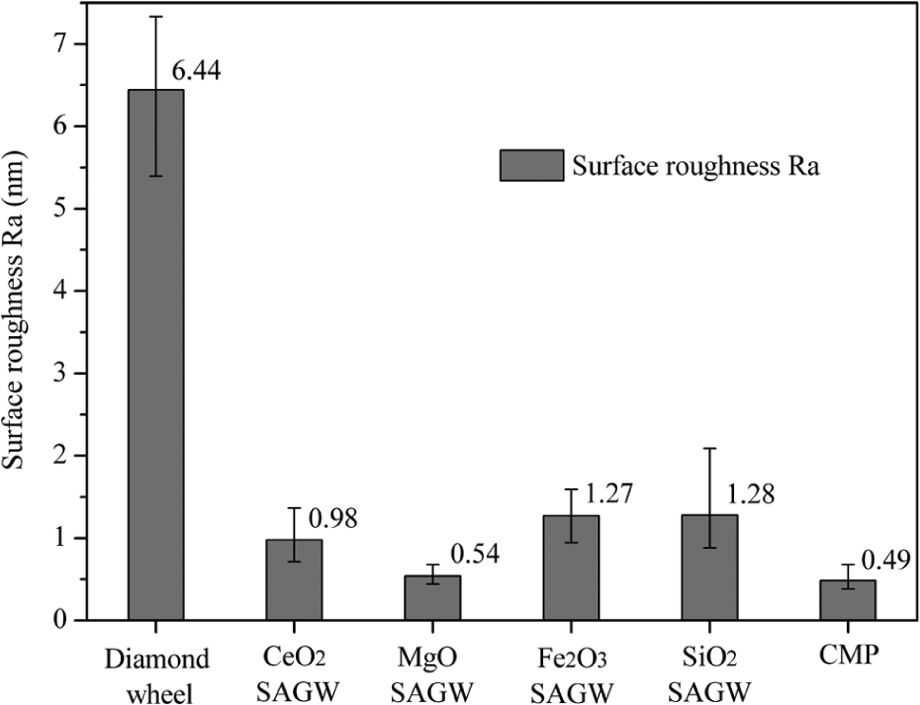
Surface roughness of the machined wafer measured by AFM.
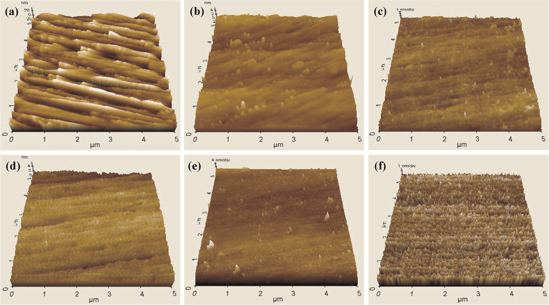
AFM images of surface topography of the silicon wafer machined by (a) conventional diamond wheel, (b) CeO2 SAGW, (c) MgO SAGW, (d) SiO2 SAGW, (e) Fe2O3 SAGW and (f) CMP.
Subsurface damage of the silicon wafer ground with the conventional diamond wheel, the SAGWs and CMP is shown in Figure 8. Subsurface damage induced by the diamond wheel was shown to be approximately 0.17 µm in depth, which consisted of 0.03 µm amorphous layer and 0.14 µm dislocation layer, as shown in Figure 8(a). On the other hand, subsurface damage generated by the four SAGWs and CMP all had only amorphous layer and was obviously smaller than that caused by the diamond wheel. The experimental study revealed that the surface/subsurface quality of the silicon wafer ground by the SAGWs was much better than that with the diamond wheel and was almost as good as that with CMP.
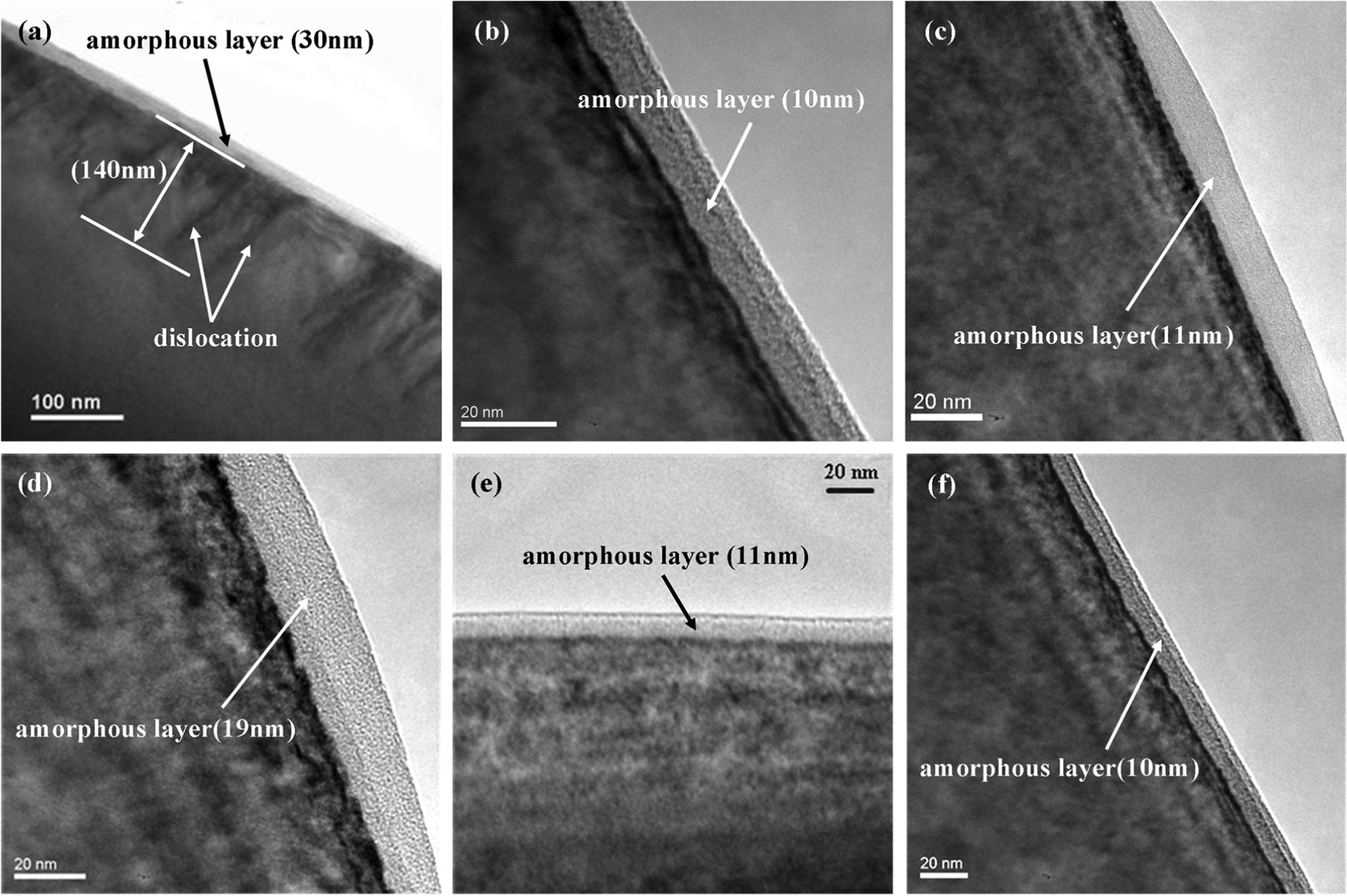
Cross-sectional TEM images of silicon wafer corresponding to (a) conventional diamond wheel, (b) CeO2 SAGW, (c) MgO SAGW, (d) SiO2 SAGW, (e) Fe2O3 SAGW and (f) CMP.
The difference of the grinding marks and subsurface damage between the SAGWs and the conventional diamond wheel is analyzed as follows. In diamond grinding of silicon, material removal is generally classified in two different modes: brittle mode and ductile mode. The brittle mode grinding is schematically illustrated in Figure 9(a). When a sharp abrasive grain gets into contact with the wafer surface, a large load is applied to the silicon. Since the contact region of the sharp abrasive grain is rather small, the tensile stress surpasses the fracture strength of silicon so as to initiate median microcracks (also called radial microcracks) and lateral microcracks at the contact point. Usually, median microcracks are associated with strength degradation in the silicon, while lateral microcracks are associated with material removal and surface formation. As the abrasive grain moves with the diamond wheel, it continuously initiates and propagates microcracks, forming the brittle chips from the wafer surface. Surface/subsurface damage is induced in the brittle mode grinding process, leaving a dimple with smooth facets and sharp ridges on the wafer surface, while in the ductile mode grinding, as shown in Figure 9(b), material is removed by the action of plastic flow, as is the case in metal, leaving a smooth and crack-free wafer surface when the removal process is performed at less than a critical DOC. However, the plastic strains are induced on the wafer surface in the ductile mode grinding, which still leads to the surface/subsurface damage in the form of grinding marks and crystal dislocation, as shown in Figure 7(a) and Figure 8(a). In this sense, grinding with the conventional diamond wheel induces distinct grinding marks and dislocation regardless of its grinding mode. On the other hand, in the CMG process, the silicon material is removed by both the mechanical action between the abrasives and silicon and the chemical action between the abrasives, additives and silicon. As the abrasives are softer than silicon, the mechanical action only removes the soft reaction layer from the wafer surface without generating deep grinding marks and dislocation, as shown in Figures 7(b)–(e) and 8(b)–(e).
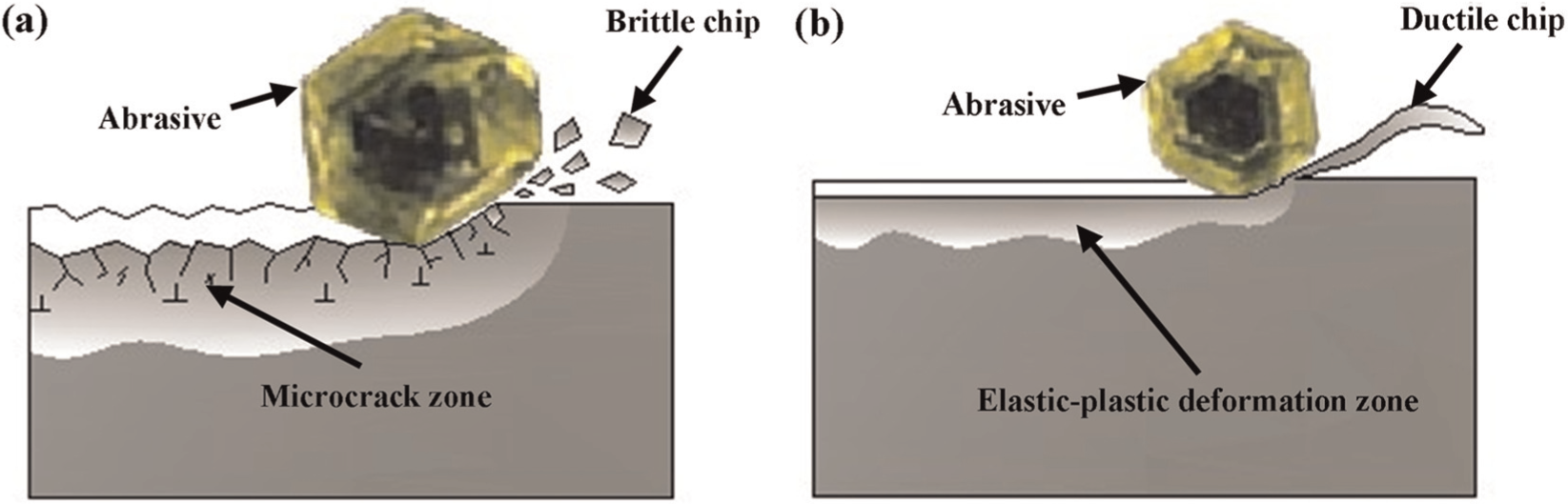
Schematic illustration of (a) brittle mode grinding and (b) ductile mode grinding.
Characteristics of SAGWs
Different periodic dressing intervals were experimentally obtained for the conventional diamond wheel and the SAGWs, as shown in Figure 10. The diamond wheel and the MgO SAGW showed better grinding durability between the consecutive dressings than the other three SAGWs. After the initial dressing, the diamond wheel and the MgO SAGW did not need a periodic dressing to complete the grinding cycles of more pieces of silicon wafer, but the other three SAGWs could not complete many grinding cycles without periodic dressings. This was especially true for the SiO2 SAGW that demanded a periodic dressing interval of 30 min, much shorter than the other SAGWs. If dressing were not provided to a grinding wheel within its periodic dressing interval, the spindle motor current, and thus the grinding force, would increase to an abnormal level, which could lead to overheating the wheel and wafer. Grinding burn would take place, which could result in damage to the grinding wheel and silicon wafer. Figure 11 shows an example of a grinding burn to an SAGW and a silicon wafer. Grinding burn marks are clearly observable from Figure 11.
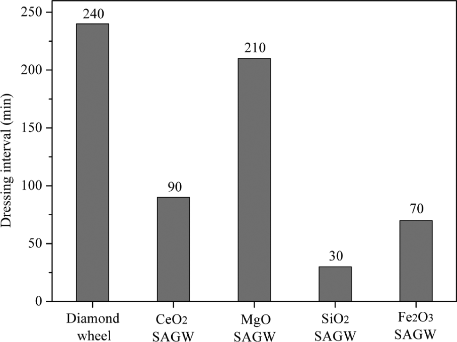
Periodic dressing intervals of the conventional diamond wheel and the SAGWs.
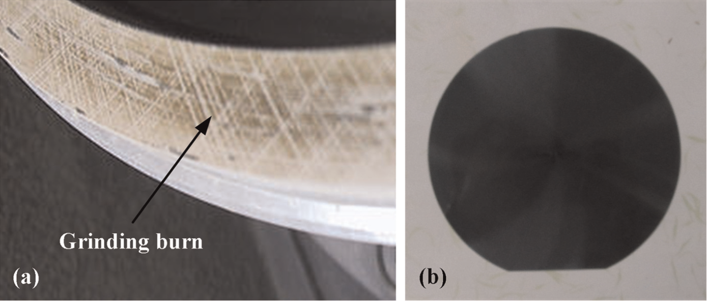
Images of (a) the burned SAGW and (b) the burned silicon wafer.
The spindle motor current, grinding ratio and MRR for the conventional diamond wheel and the four SAGWs are shown in Figures 12 and 13. From Figure 12, it is found that the spindle motor current in using the four SAGWs is in the range of 7.5–8.0 A, which is higher than that for the diamond wheel (6.5 A). The SAGWs also showed a much lower MRR and grinding ratio than the diamond wheel, as shown in Figure 13. Two reasons are considered. The first reason is that for the SAGWs, CeO2, MgO, SiO2 and Fe2O3 abrasives have their hardness either comparable to or lower than that of silicon. The second reason is the high porosity ratio in the SAGWs. The low hardness abrasives and high porosity ratio inevitably reduce the cutting ability and wear resistance of the SAGWs, leading to reduced MRR and grinding ratio. Nevertheless, the newly designed SAGWs had their MRR better than that of CMP. On the other hand, this study found that the MgO SAGW demonstrated the highest MRR of the four SAGWs although the MgO abrasive was softer than the CeO2, SiO2 and Fe2O3 abrasives. This conflicts with the conventional grinding theory in that the higher the hardness of an abrasive, the better the cutting ability of the abrasive. MRR of the grinding wheel with the harder abrasive should also be higher. Unfortunately, the conventional grinding theory did not take into account the chemical effect of the abrasives on silicon wafer. In fact, chemical effect can make a considerable contribution to the material removal in a grinding process. Although the MgO abrasive was not superior to the other three abrasives in terms of hardness, it demonstrated the highest chemical affinity with silicon, which enhanced material removal in the silicon wafer grinding process, and provided the highest MRR of the four SAGWs.
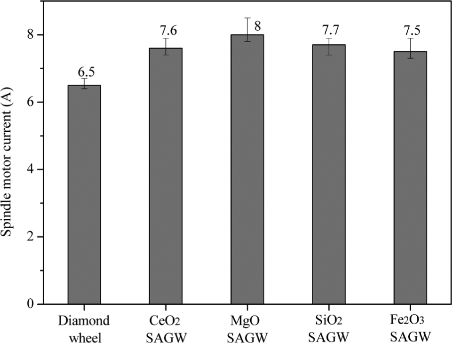
Spindle motor current for the conventional diamond wheel and the SAGWs.
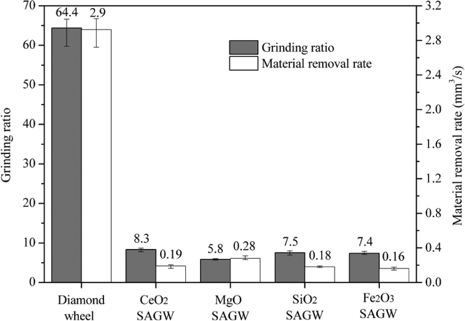
Grinding ratio and MRR for the conventional diamond wheel and the SAGWs.
Conclusion
This study experimentally has demonstrated that CMG is a promising technique in finishing silicon wafers with high quality and efficiency. In this study, four SAGWs with different soft abrasives are newly designed, tested and compared with the conventional diamond wheel and CMP in terms of grinding quality, dressing interval, grinding current, grinding ratio and MRR. The results obtained are summarized in the following:
The newly designed SAGWs are all comparable to CMP and better than the diamond wheel in terms of wafer grinding quality.
The SAGWs show lower cutting ability and wear resistance than the diamond wheel but higher MRR than CMP.
For the newly designed SAGWs, the MgO SAGW is the best in grinding quality, dressing interval and MRR.
Footnotes
Funding
The authors are grateful to the financial support for this research from the National Science Foundation of China (Grant numbers 91023019 and 91023043) and the State Key Development Program for Basic Research of China (Grant number 2011CB013201).