
Abstract
The uniformity of the alignment-layer thickness on indium tin oxide glass plays an important role in producing liquid crystal display panels of quality images. However, thickness non-uniformity results in producing liquid crystal display panel of poor color image, which increases rework cost and scrap. The Taguchi method is utilized in the define–measure–analyze–improve–control approach to improve the capability of this process. In the define phase, process mapping and quality characteristic definition are discussed. The x̄ and R control charts and process capability analysis are employed in the measure phase. The L18 array and signal-to-noise ratio, followed by analysis of variance, are utilized in the analyze phase. In the improve phase, two-step optimization is conducted to reduce thickness variations and adjust process mean on target. The control charts for the thickness are regularly constructed in the control phase. Initially, the estimates of the capability indices for the alignment-layer printing process are 0.731 and 0.69, respectively, which indicate that this process is incapable. Utilizing the Taguchi method, confirmation experiments showed that the potential and actual capability indices are respectively improved to 3.48 and 3.47. Hence, the process becomes highly capable. This proves the effectiveness of the Taguchi method in improving the performance of the alignment-layer printing process.
Introduction
In an information-dominated age, the display of information is becoming increasingly essential in many aspects of daily life. Owing to several important characteristics, such as lightweight, low radiation, and low power consumption, the liquid crystal display (LCD) has become one of the most important systems for high performance information displays. 1 The LCD panel has created a new reality in the electronic information displays industry; such as, television, mobile phones, laptop computers, digital cameras, and other consumer-related communications hardware.
Basically, the LCD consists of a thin-layer liquid crystal sandwiched between a pair of polarizers. To control the optical transmission of the display element (pixel; picture element), the liquid crystal layer is placed between transparent electrodes, which are usually indium tin oxide (ITO) owing to its higher conductivity. In a liquid crystal cell without any external field, the ordering of the molecules is usually determined by the anisotropy of the boundary. Thus, the surfaces of the electrodes or ITO are usually coated with an alignment layer (e.g. polyimide) evenly. The uniformity of the alignment-layer thickness on ITO glass plays an important role in producing panel displays of quality images. In practice, thickness non-uniformity results in color aberration, causes difficulties in assembly process, and increases rework cost scrap. As a result, manufacturing costs of the LCD panel are increased. Therefore, in this research, process engineers aim at improving the capability of the alignment-layer printing process.
Six sigma 2 is a project-driven management approach to improve the organization’s products, services, and processes by continually reducing defects in the organization. Six sigma focuses on improving customer requirements’ understanding, business profitability, and the effectiveness and efficiency of all operations to meet or exceed customer’s needs and expectation. 3 A widely accepted six sigma approach is the define–measure–analyze–improve–control (DMAIC) approach, 4 which has been adopted to improve the performance and quality for numerous manufacturing processes.5,6 The DMAIC approach adopts several tools for quality improvement, 7 including process mapping in the define phase, the capability analysis in measure phase, analysis of variance (ANOVA) in the analyze phase, the robust design in the improve phase, and the control charts in the control phase. This research, therefore, employs the DMAIC approach to enhance the performance of the alignment-layer printing process, and then summarizes.
The define phase
This research is conducted on the cell process for the thin film transistor LCD (TFT-LCD) panel. The TFT-LCD panel is simply composed as shown in Figure 1(a) of two glass substrates sandwiching a layer of liquid crystal. The color filter gives each pixel its own color and is fitted with the front glass substrate. The transistors are fabricated on the back glass substrate. A light source is located at the back of the LCD panel. When a voltage is applied to the transistor, the liquid crystal is bent allowing light to pass through to form a pixel. Typically, a TFT-array substrate is composed, as seen in Figure 1(b), of a matrix of pixels and ITO region each with a TFT switching device, which functions to turn each individual pixel on or off. To create the display image, thousands or millions of pixels are needed.
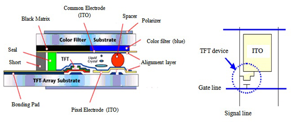
Illustration of the LCD structure. (a) The basic structure of LCD. (b) The sketch of TFT substrate.
Two tasks are conducted in the define phase.
Mapping the alignment-layer printing process.
Defining the key quality characteristic (QCH).
Mapping the alignment-layer printing process
The production line of TFT-LCD panels is depicted in Figure 2. As seen in this figure, three main processes are performed in this line; i.e. the array, cell, and module processes. The array process involves cleaning glass substrates, photo-resist coating, and exposure and developing, repeated several times. In the cell process, which is a special step in the LCD manufacturing, the color filter and TFT-array substrate pass through cleaning, alignment-layer printing, and rubbing. Finally, in the module process, the color filter and TFT panel are aligned, combined and fixed together using ultraviolet (UV)-hardened polymer spots. The liquid crystal is then injected between the two ITO layers and the LCD product is completed by adding the back-light unit, intergrated circuit (IC), and other components.
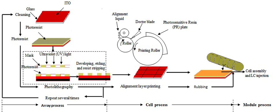
The main processes of LCD line.
Research on the TFT-LCD panel manufacturing process is comparatively incomplete. Lin et al. 8 proposed an analytical framework for TFT-LCD production chain planning and scheduling. Ishihara 9 discussed some mechanisms for the liquid crystal alignment and reviewed various alignment techniques and methods to investigate the interaction of the liquid crystal molecules with substrates. Chen et al. 10 improved the photo-resist coating, which is the main process in the array process, of the TFT-LCD panel using a capability assessment model and the measure–analyze–improve–control approach. However, this research investigates the cell process and mainly focuses on the alignment-layer printing process.
The alignment-layer printing process is displayed in Figure 2, which can be described as follows. A doctor blade distributes a layer of the alignment-layer liquid (polyimide) on a carry-roll, which is then transferred to the printing roll. The printing roll transfers a desired pattern of photosensitive resin (PR) plate gravures filled with a volume of polyimide liquid on ITO glass evenly. The three-dimensional (3D) and two-dimensional (2D) images for the surface of PR plate taken using the classic measuring system are depicted in Figure 3(a) and (b), respectively.
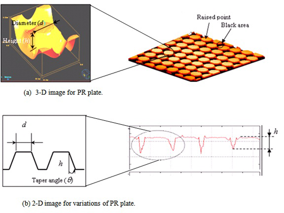
The 3D and 2D images for PR plate.
In Figure 3, the main problem is summarized by the excessive variations of the PR plate; i.e. the variations contributed by the diameter (d), height (h), and taper angle (θ), which result in non-uniformity of the alignment-layer thickness. In practice, the non-uniformity of the alignment-layer thickness results in color aberrations in the LCD’s image; i.e. color saturation, shades, brightness, and contrast. In addition, it causes difficulties in the assembly process. As a result, the main objective of this research is to enhance the capability of the alignment-layer printing process by reducing the variations contributed by d, h, and θ.
Identifying the critical QCH
For the alignment-layer printing process, the key measurable and continuous QCH is the alignment-layer thickness, which is the nominal-the-best type. The desired target (T) of thickness is 700 Å, while the upper and lower specification limits, USL and LSL, are 800 Å and 600 Å, respectively. Practically, a layer thickness above the USL results in insufficient LCD color saturation, or pixel brightness, while below the LSL limit causes oversaturated color, or pixel darkness. As thousands of pixels create the LCD image, color shades may occur. Such quality defects, in reality, cannot be reworked and, hence, the LCD would be scrapped.
The measure phase
In this phase, the
The x̄ and R control charts
The
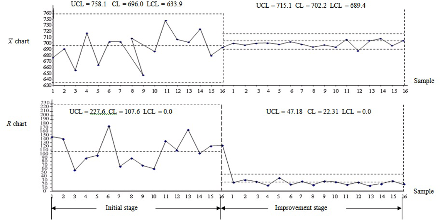
Control charts at initial and improvement stages.
The lower control limit (LCL), center line (CL), and upper control limit (UCL) for the
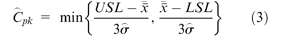
Process capability analysis
Process capability analysis is a vital part of an overall quality-improvement program, by which the capability of a manufacturing process can be measured and assessed. The potential and actual process capability indices,

In practice, the process standard deviation (σ) is unknown and frequently estimated by

where
where
In Figure 4, the
The analyze phase and improve phase
The Taguchi method15–16 is widely used in quality engineering for analyzing and improving quality and yield. The main goal of this method is finding the optimal setting of control factors involved in a system to make its performance insensitive to noise, and thus it has been utilized in many business applications; such as, chip-on-board technology, 17 surface mounting technology, 18 and the SUS304 wire drawing process. 19 The Taguchi method is utilized in the analyze phase and improve phase as described in the following subsections.
The analyze phase
Three tasks are carried out for analyzing the experimental data of the alignment-layer thickness. These tasks are described as follows.
The orthogonal array experiments
The cause and effect diagram for thickness non-uniformity is shown in Figure 5. Notice that the variations contributed by the diameter, height, and taper angle of the PR plate are the main causes for thickness non-uniformity. These variations can be controlled by four cell process factors, including: arrangement method of the alignment-layer molecules on the ITO surface (x1), molecule diameter (x2), UV exposure energy (x3), and UV exposure time (x4).
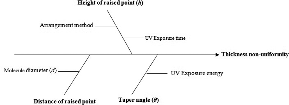
Cause and effect diagram for thickness non-uniformity.
Based on process knowledge, factor A is assigned at the two levels as illustrated in Figure 6, whereas factors B to D are assigned each at three levels. The level values for these factors are displayed in Table 1. The alignment-layer printing process is performed at the initial factor settings A1B1C1D1.
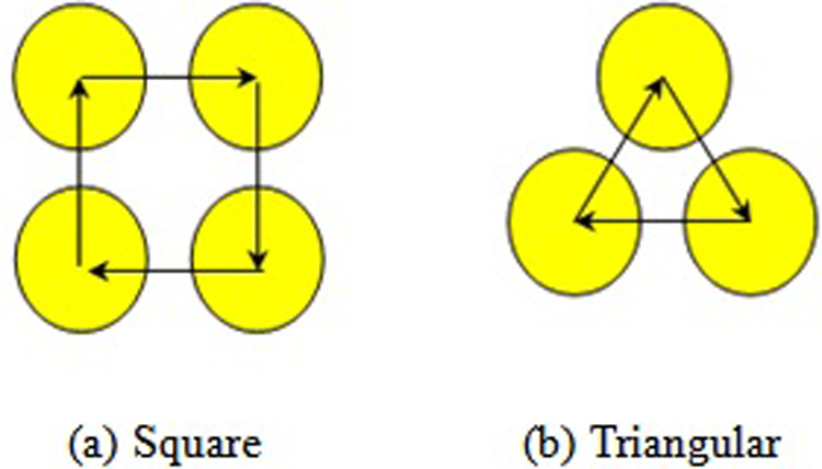
Illustration of the arrangement method.
The control factors and their levels.
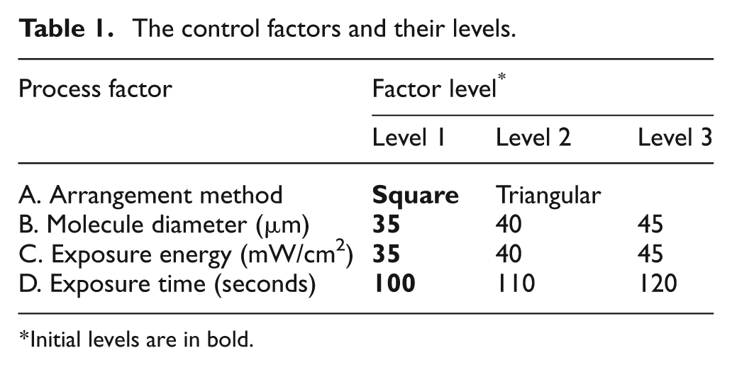
Initial levels are in bold.
An efficient way to study the effect of several control factors simultaneously is to plan matrix experiments using orthogonal arrays (OAs). The appropriate OA to investigate a two-level factor and three three-level factors is the L18 (21 × 37) array shown in Table 2. In this array, factor A is assigned to column 1; since it has two levels. Factors B, C, and D are assigned to the next three three-level columns, respectively. The other four columns are left empty for evaluating error term.
The experimental results using L18 array.
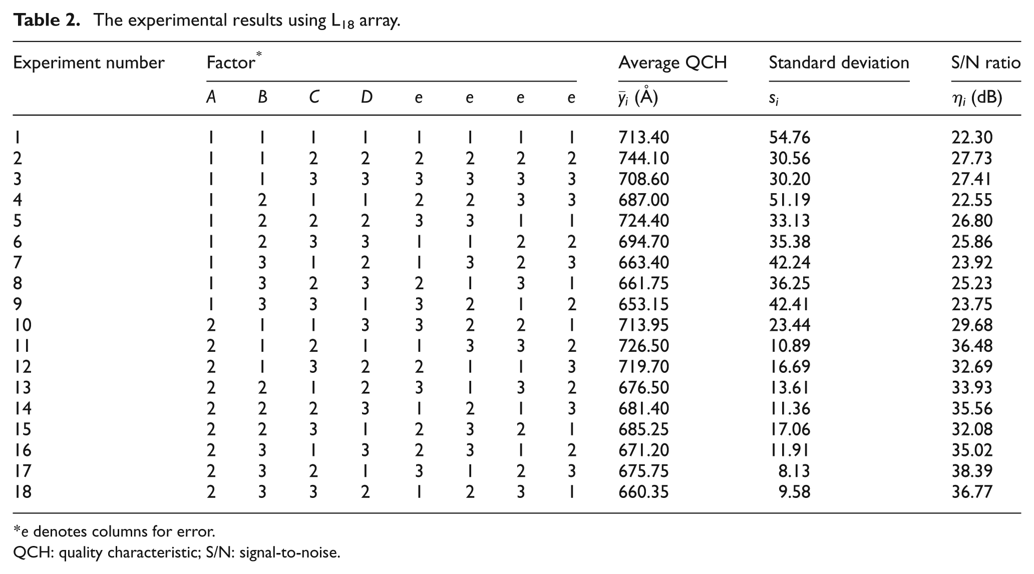
e denotes columns for error.
QCH: quality characteristic; S/N: signal-to-noise.
Preliminary experiments are conducted to ensure the measuring instruments are repeatable and capable. Next, the 18 experiments in the L18 (21 × 37) array are performed by varying the factor levels in a systematic manner. Four repetitions are conducted at the same factor levels of each experiment. The thickness is then measured at five different places on the surface of the ITO sample.
Signal-to-noise ratio analysis
The signal-to-noise (S/N) ratio (η) is always used in the Taguchi method to interpret experimental data and measure performance. For the nominal-the-best type QCH, η i is calculated for each experiment i using
where
The

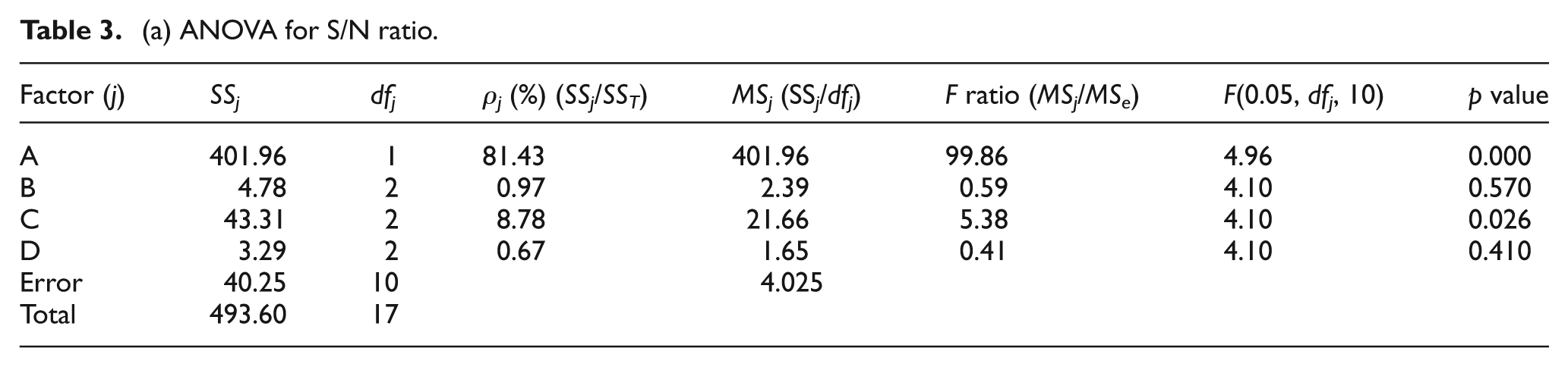
The results of ANOVA for the S/N ratio are summarized in Table 3.
(a) ANOVA for S/N ratio.
(b) ANOVA for S/N ratio (after pooling insignificant factors).
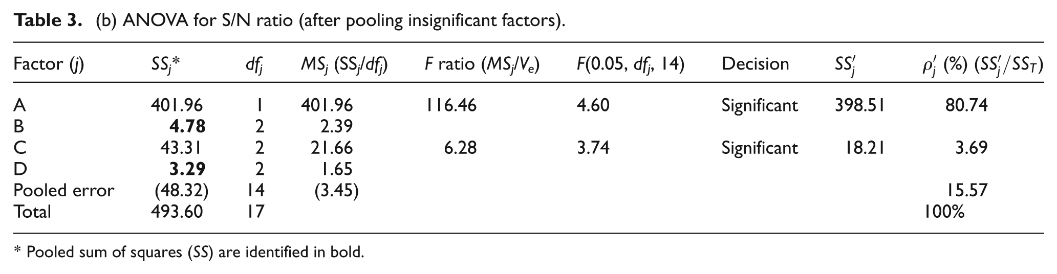
* Pooled sum of squares (SS) are identified in bold.
It is noticed in Table 3(a) that the ρA (= 81.43%) and ρC (= 8.78%) contribute more than 5% to total variation, whereas ρB (= 0.97%) and ρD (= 0.67%) contribute less than 5%. The F ratio is calculated for each factor then compared with the F value at 5% significance level. That is, the F ratio for factor A (= 99.87) is compared with F0.05,1,10 (= 4.96), whereas the F ratios correspond to factors B to D are compared with F0.05,1,10 (= 4.10). If the F ratio of a factor is larger than the F value at 5% significant level, this factor is judged significant; otherwise, it is considered insignificant. Based on F testing, the effects of factors A and C are considered significant. However, the effects of factors B and D are judged insignificant, and hence they will be pooled into the error term. The ANOVA results for the S/N ratio after pooling factors B and D are shown in Table 3(b). In this table, the degrees of freedom associated with pooled error are increased to 14, which is calculated as the degree of freedom of error (= 10), plus the degrees of freedom corresponding to pooled factors B and D. Consequently, the F ratios of factors A and C are calculated by dividing the mean square of each factor by the pooled error mean square (Ve). The F ratios are then compared with F0.05,1,14 (= 4.60) and F0.05,2,14 (= 3.74) for factors A and D, respectively. These factors are found still significant. Let ρ′j denote the pure percentage contribution by factor j calculated as

where SS’j is the pure sum of squares contributed by factor j with degrees of freedom (dfj), which can be estimated using

For example, the ρ′A is calculated as follows. The dfA and Ve are equal to 1.00 and 6.90, respectively. Substituting these values in equation (7), the SS’A is then

Using equation (6), the ρ′A is estimated as

The ρ′A value indicates that 80.74% of the total variation is contributed by the arrangement method of the surface molecules (factor A). Therefore, factor A is considered the most influential factor on variation reduction. The ρ′C (= 3.69%) is calculated in a similar manner.
The results of ANOVA for the S/N ratio are summarized in Table 4, where the ρA and ρD values are calculated 0.72% and 2.51%, respectively, which are less than 5%. While, the molecule’s diameter (factor B) has the largest contribution (ρ′B = 78.62%) to the total variations followed by contribution of the exposure energy (factor C), ρ′C, of 7.37%. The F ratios of factors B and C of 36.47 and 3.42, respectively, are compared with the F values at 5% significance level, F0.05,2,13 (= 3.81). Obviously, only factor B significantly affects the thickness mean, while it does not affect the S/N ratio. Hence, this factor will be used to adjust process mean on target.
ANOVA for thickness.
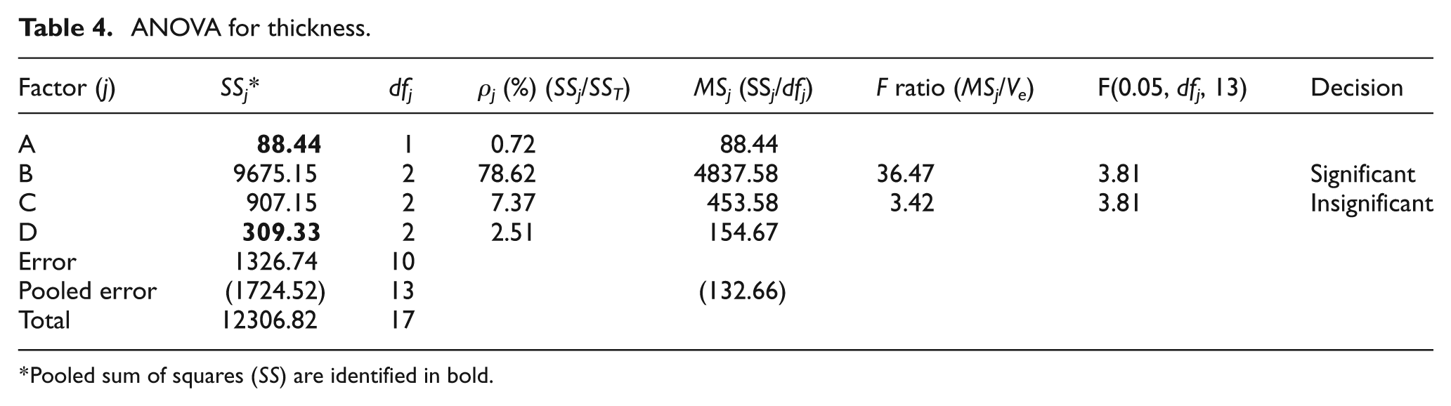
Pooled sum of squares (SS) are identified in bold.
The improve phase
Taguchi’s two-step optimization is conducted in this phase to improve the alignment-layer printing process. The first optimization step aims at reducing variation, whereas the second one considers adjusting the process mean on the desired target (= 700 Å).
Variation reduction
Reducing variation is accomplished by choosing the factor levels that maximize the S/N ratio. Factors A and C are found to significantly affect variability. The S/N ratio averages for each factor levels are summarized in Table 5 and then depicted in Figure 7. It is observed that the combination of optimal factor levels that reduces variability is A2C2.
S/N ratio averages for each factor level.
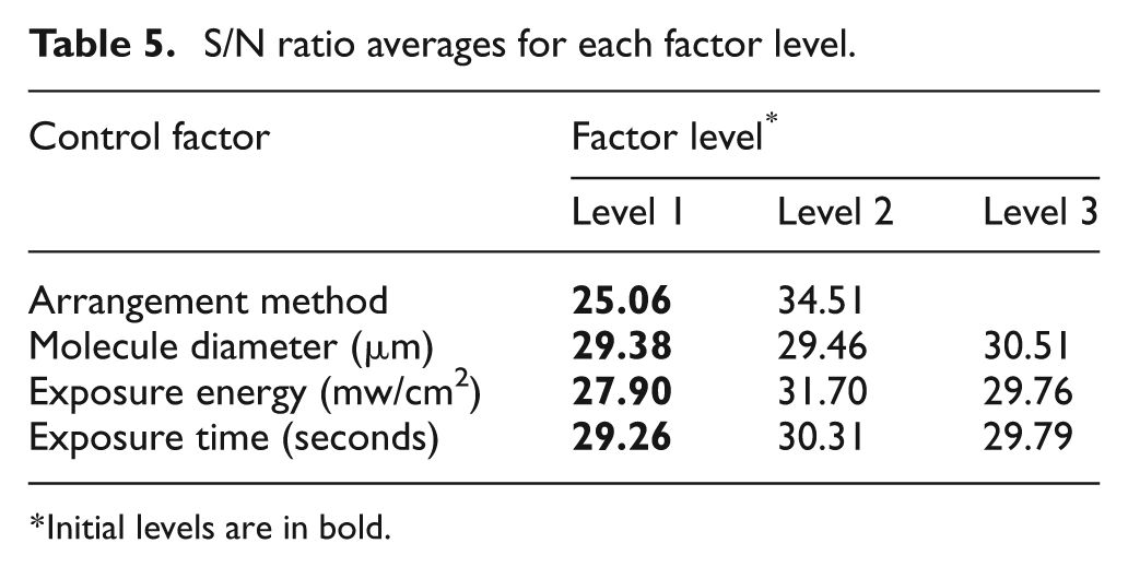
Initial levels are in bold.
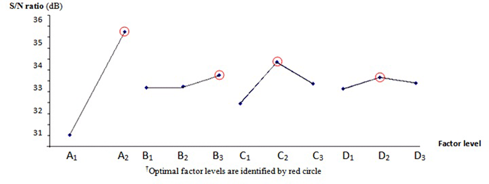
Average S/N ratio plot.
To confirm the improvement gained by setting factor A and C levels A2C2, two ITO samples, each of size 300 mm × 400 mm, are randomly selected per day for eight working days, which results in 16 ITO samples. The alignment-layer thickness is measured using the contour measuring instrument at five different places on the surface of each ITO sample. The
Adjustment of the process mean on target
Process mean can be adjusted on the target by selecting the factors that have significant effects on the mean but practically no effect on η. Previously, it is concluded that the molecule diameter (factor B) is only factor for this purpose. Therefore, factor B is used to adjust the process mean on target. Table 6 displays the thickness averages for each factor level.
QCH averages for each factor level.
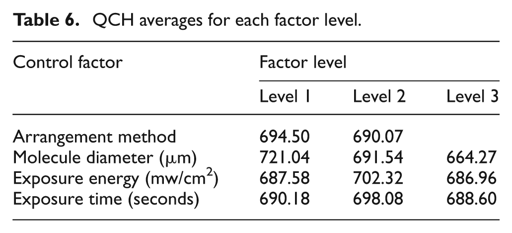
In Table 6, the thickness average decreases as the level value of factor B increases. In order to reduce the process mean from 702.2 to 700 Å, the best level value of factor B is calculated by interpolation and found equal to 35.37 µm, which is calculated as the value of level 1 (= 35) plus the difference between thickness averages at level 1 and 2 divided by 2.2. Confirmation experiments are finally conducted at the level value of 35.37 µm for factors B and A2C2. Confirmation results show that the process mean is 700.20 Å, while the σ̑ value is not affected. The
The control phase
In this phase, the
Conclusions
Image color-quality has been recognized as one of the top considerations in the display manufacturing industry and has become a benchmark that influences the consumers’ purchasing decision. At the initial stage, the
Footnotes
Funding
This research received no specific grant from any funding agency in the public, commercial, or not-for-profit sectors.